UNIVERSIDADE DE LISBOA
FACULDADE DE CIÊNCIAS
DEPARTAMENTO FÍSICA
Low Noise Power Supplies for the High Voltage Board of the
TILECAL Calorimeter
Rui Paulo Serrano Fernandez
Mestrado Integrado em Engenharia Física
Dissertação orientada por:
Acknowledgments
Firstly, I want to thank my family for their understanding and support over the last five years, especially my parents who were always present when I needed them and my sister who brought me to places I didn’t know, which allowed me forget a little of the pressure the university brings. To my classmates, who made the course not only a place to learn but to grow as a person. To Professor Guiomar Evans for giving me the opportunity to participate in this spectacular project, which allowed me to learn much more than I had expected, for supporting me since then, always available to help and for being my advisor.
I also want to thank Professor Jos ´e Augusto for being always available to answer my ques-tions. To Luis Gurriana who helped me a lot throughout the project in using a program I didn’t know. To all the teachers who over the past 5 years have given me all the information I needed to be able to complete this thesis and be ready for the next step, the world of work. And to the University of Lisbon for providing a favourable environment for my development, both as a person and a student.
I want to leave a special thank you to my closest group of friends, who made my college life more bearable and fun and helped me when I needed it most, especially In ˆes Albuquerque who was present since the beginning of my academic life. She was always there to offer me help even when she needed it too, and in recent months especially where we both had a difficult time due to the thesis, but the fact that she was present made me believe that I could finish the course and push me to continue even when I no longer wanted to.
Finally, I want to thank all the people I could not refer to but who have been by my side for these 5 long years and have been my moral support. The university is not easy but it is still worth it and especially if we are lucky enough to know and accompany people who make their mark in our life, without them none of this would be possible.
Resumo
O sistema atual de distribuic¸ ˜ao de alta tens ˜ao do calor´ımetro hadr ´onico central da ex-peri ˆencia ATLAS do CERN, TileCal, foi fabricado no final dos anos 90. Este foi projetado para estar em funcionamento durante 10 anos, no entanto j ´a se encontra em funcionamento h ´a cerca de 20 anos. Atualmente, muitos dos componentes utilizados encontram-se obsoletos o que impossibilita a sua reparac¸ ˜ao e reutilizac¸ ˜ao. Por outro lado, o sistema atual encontra-se no interior da caverna ATLAS, logo encontra-encontra-se exposto a altos n´ıveis de radiac¸ ˜ao. Esta exposic¸ ˜ao cont´ınua a altos n´ıveis de radiac¸ ˜ao resultantes das colis ˜oes entre os feixes de part´ıculas, que ocorrem no LHC (Large Hadron Collider), afeta todo o sistema. O facto de o sistema se encontrar na caverna suscita ainda outros problemas, tais como, a dificuldade de reparar ou mesmo substituir qualquer componente ou placa constituinte do sistema eletr ´onico, danificado pela radiac¸ ˜ao ou devido ao envelhecimento eletr ´onico. Para se efetuar a reparac¸ ˜ao ou a substituic¸ ˜ao de componentes ou placas ´e necess ´ario que o LHC pare o seu funciona-mento durante alguns meses, de modo a que os n´ıveis de radiac¸ ˜ao diminuam o suficiente para permitir que um t ´ecnico possa entrar na caverna, por ´em esta pausa de meses s ´o oferece um tempo muito limitado para executar esta tarefa.
Para al ´em destes problemas tem-se ainda como um dos objetivos o aumento da luminosi-dade do LHC, o que vai implicar um aumento do n´ıvel de radiac¸ ˜ao na caverna ATLAS. Outro dos objetivos, ´e a diminuic¸ ˜ao do intervalo de tempo entre as colis ˜oes de part´ıculas, levando `a necessidade de eletr ´onica mais r ´apida. Todos estes problemas e novos objetivos fazem com que seja necess ´ario atualizar e/ou modificar toda a electr ´onica do TileCal.
De forma a superar estes problemas, foi proposta uma atualizac¸ ˜ao: um novo sistema de distribuic¸ ˜ao de alta tens ˜ao (HVDS) ser ´a colocado fora da caverna onde se encontra o detetor, passando este a ser um sistema remoto que n ˜ao ´e afetado pela radiac¸ ˜ao, maximizando assim a fiabilidade e a robustez do sistema. A eletr ´onica deste novo sistema ser ´a colocada numa sala sem radiac¸ ˜ao, localizada 100 metros acima da caverna ATLAS, o que permitir ´a o acesso permanente ao sistema de distribuic¸ ˜ao de altas tens ˜oes. Assim, deixa de ser necess ´aria a exist ˆencia de uma paragem do funcionamento do LHC para executar reparac¸ ˜oes no sis-tema. Outra vantagem inerente ao sistema remoto ´e deixar de haver uma limitac¸ ˜ao de tempo dispon´ıvel para realizar as reparac¸ ˜oes e/ou substituic¸ ˜oes, diminuindo tamb ´em o risco a que o t ´ecnico est ´a sujeito quando as executa. Para este novo sistema ´e necess ´ario produzir uma placa dedicada que fornec¸a as alimentac¸ ˜oes prim ´arias necess ´arias, alta e baixa tens ˜ao, dado que no sistema atual as fontes de alimentac¸ ˜ao prim ´arias de baixa tens ˜ao encontram-se na caverna ATLAS e as de alta tens ˜ao embora se encontrem na sala sem radiac¸ ˜ao j ´a referida s ˜ao fontes lineares de elevado custo.
O trabalho apresentado nesta dissertac¸ ˜ao insere-se na colaborac¸ ˜ao portuguesa no projeto ATLAS/CERN. Este consiste no desenvolvimento de uma placa de alimentac¸ ˜ao, designada por Power Supplies, capaz de fornecer tanto a alta tens ˜ao (HV), −830 V a −950 V, como as baixas tens ˜oes ,±12 V e 3, 3 V, sendo imperativo que todas as tens ˜oes produzidas tenham baixo ru´ıdo.
dois dos conversores DC/DC s ˜ao utilizados para produzir a alta tens ˜ao, −830 V a −950 V @ 10mA, e os restantes dois para as baixas tens ˜oes, um para os 3.3 V @ 0.8 A, e o outro que ´e um conversor DC/DC duplo para os ±12 @ 2.5 A. Cada HVDS fornece a alimentac¸ ˜ao para 48 fotomultiplicadores (PMTs) do detetor. Devido `a corrente necess ´aria para alimentar todos os PMTs, ´e necess ´ario recorrer ao uso de dois conversores DC/DC para produzir a alta tens ˜ao.
Os valores da tens ˜ao de sa´ıda dos conversores DC/DC de alta tens ˜ao s ˜ao controlados digitalmente, podendo fornecer dois valores diferentes, −830 V ou −950 V. Estes valores de tens ˜ao distintos permitem que cada PMT do detetor possa receber a tens ˜ao adequada para funcionar corretamente. Dado que n ˜ao existe um ´unico componente que seja igual a outro, cada PMT ter ´a as suas caracter´ısticas pr ´oprias e, portanto, a sua tens ˜ao de alimentac¸ ˜ao deve ser ajustada para se obter o melhor desempenho do detetor. Estes dois valores de tens ˜ao permitem a correta calibrac¸ ˜ao de todos os PMTs efetuada pelo sistema de distribuic¸ ˜ao das altas tens ˜oes.
A placa que fornecer ´a as alimentac¸ ˜oes ao HVDS, dever ´a ainda oferecer algumas funcional-idades extra, tais como: a possibilidade de uma monitorizac¸ ˜ao em tempo real do consumo em tens ˜ao e corrente de cada conversor, a leitura da temperatura em dois pontos diferentes da placa, a capacidade de ligar/desligar digitalmente cada um conversores DC/DC individual-mente e ligar/desligar manualindividual-mente todos os conversores DC/DC ao mesmo tempo, atrav ´es de um interruptor. Este ´ultimo servir ´a como medida de seguranc¸a caso o m ´etodo digital n ˜ao funcione ou em caso de substituic¸ ˜ao ou manutenc¸ ˜ao do sistema sem necessidade de recorrer ao sistema de controlo digital do ATLAS.
O controlo disgital da placa Power Supplies ser ´a baseado num protocolo de comunicac¸ ˜ao SPI e num expansor s ´erie/paralelo. O sinais de sa´ıda do referido expansor ser ˜ao os sinais para ligar/desligar os conversores, os sinais de selec¸ ˜ao de tens ˜ao de sa´ıda dos conversores de alta tens ˜ao e os sinais que permitem a leitura adequada e em tempo real dos consumos de tens ˜ao e de corrente e dos sensores de temperatura utilizados. Estas leituras s ˜ao efetuadas recorrendo ao controlo digital de um multiplexador anal ´ogico e a um conversor anal ´ogico digital (ADC).
Ainda no ˆambito desta tese, ´a apresentada a interface gr ´afica de utilizador (GUI) desen-volvida na linguagem de programac¸ ˜ao Python. Esta foi utilizada para facilitar a comunicac¸ ˜ao entre a placa Power Supplies e o utilizador. A interface gr ´afica est ´a dividida em tr ˆes secc¸ ˜oes diferentes, de forma a ser mais intuitiva para o utilizador. A primeira secc¸ ˜ao ´e a secc¸ ˜ao re-spons ´avel por ligar/desligar os conversores DC/DC, sendo que esta apresenta quatro caixas de selec¸ ˜ao, uma para cada conversor, que quando selecionadas pelo utilizador, executam o c ´odigo respons ´avel por enviar a instruc¸ ˜ao ao expansor para enviar o sinal de ligar/desligar para os conversores DC/DC selecionados. Na segunda secc¸ ˜ao encontram-se representadas duas barras deslizantes, `as quais se encontra associado um cursor que se pode deslocar entre duas posic¸ ˜oes distintas, associadas `a selecc¸ ˜ao da tens ˜ao de sa´ıda de cada um dos conver-sores DC/DC de alta tens ˜ao. Associada `a posic¸ ˜ao do cursor encontra-se tamb ´em um texto informativo que permite que o utilizador verifique se a tens ˜ao seleccionada ´e a pretendida.
A terceira e ´ultima secc¸ ˜ao ´e a da leitura dos consumos de tens ˜ao e de corrente assim como das duas temperaturas lidas por dois sensores de tempertura colocados em pontos disntintos da carta. Esta leitura pode ser feita de duas formas diferentes, pode ser feita uma ´unica medida atrav ´es da selec¸ ˜ao de bot ˜oes dedicados que apenas permitem selecionar uma opc¸ ˜ao de cada vez, sendo o resultado da leitura apresentado em duas caixas. A primeira caixa com a leitura em contagens do ADC, que ´e o valor que o ADC fornece diretamente, e a segunda caixa com a leitura do valor correspondente ao que se est ´a efetivamente a medir com a respetiva unidade fisica. A outra forma envolve um conjunto v ´arias medic¸ ˜oes continuas de uma das grandezas anteriormente referidas, sendo que o utilizador pode escolher o n ´umero de medic¸ ˜oes pre-tendidas e o intervalo de tempo entre cada medida. Os valores lidos/medidos atrav ´es deste m ´etodo s ˜ao apresentados em gr ´aficos diferentes em func¸ ˜ao do tempo atualizados em tempo real, sendo poss´ıvel guardar estes dados num ficheiro do tipo csv.
O trabalho desta dissertac¸ ˜ao consistiu no desenvolvimento de uma placa que ir ´a fornecer as alimentac¸ ˜oes prim ´arias necess ´arias para o novo sistema de distribuic¸ ˜ao de alta tens ˜ao, e no desenvolvimento da interface gr ´afica de utilizador dedicada para esta placa que permitir ´a o seu teste funcional e que ser ´a mais tarde migrada para o teste de controlo digital do ATLAS.
Abstract
The current system that distributes high voltage to the hadronic calorimeter TileCal of the AT-LAS experiment at CERN was manufactured in the late 1990s and now many of its components are obsolete. In addition to this, the continuous exposition to high levels of radiation that results from the LHC collision affects the whole system. The calorimeter itself will be upgraded and a faster and low noise electronic will be needed. Given this, an update was proposed to mitigate these problems: a new high voltage distribution system (HVDS) placed outside of the detector, a remote system which will not be affected by the radiation, that maximize the reliability and robustness of the system. For this new system it is necessary to produce a dedicated board that provides the necessary primary supplies. Therefore, the presented work consists in the development of a power supply board capable of providing both high voltage (HV), −830 V and −950 V, and low voltage, ±12 V and 3.3 V, with low noise, resorting to DC/DC converters. Each HVDS provides the supply to 48 photomultipliers tubes (PMTs) of the detector. Due to the current needed, two high voltage sources are available, each one to supply just half of the PMTs. The values of the provided HV supplies are digitally controlled to one of the referred values, so each PMT of the detector can receive the right voltage to work correctly. Besides that, this board is controlled by a serial peripheral interface (SPI) communication protocol and has an analog to digital converter (ADC) and an analog multiplexer that are used to provide the user monitoring of all supply voltages and currents in real-time as well as the temperature, in two different positions of the board, in real time. A graphical user interface (GUI) has also been developed which allows easy communication between the power supply board and the user.
Keywords:
CERN, ATLAS, Power Supply, Low Noise, TileCal, PMTs (acronym ofpho-tomultipliers tubes), SPI (acronym of serial peripheral interface), ADC (acronym of analog to digital converter).
Contents
Acknowledgments . . . iii
Resumo . . . v
Abstract . . . viii
List of Figures . . . xi
List of Tables . . . xiii
Nomenclature . . . xv
1 Introduction 1 1.1 ATLAS Experiment . . . 1
1.2 Current High Voltage Distribution System . . . 4
1.3 High Voltage Distribution System Upgrade . . . 5
1.4 Proposed Power Supplies Board . . . 6
2 Power Supplies Board 8 2.1 Project . . . 9
2.1.1 Enable/Disable of the DC/DC Converters . . . 13
2.1.2 Real-Time Consumption Readings . . . 16
2.1.3 Temperature Reading . . . 18
2.2 Printed Circuit Board . . . 20
3 User Interface and Communication with Power Supplies board 26 3.1 Communication Protocol . . . 27
3.2 Power Supplies Graphic User Interface . . . 30
3.2.1 Connection Between User Interface and Raspberry Pi . . . 31
3.2.2 Port Expander . . . 34
3.2.3 ADC and Multiplexer . . . 37
3.2.4 Enable/Disable of DC/DC Converters . . . 37
3.2.5 Set the Output Voltage of HV Converters . . . 39
3.2.6 Reading Functionality . . . 40
4 Functional Tests 48 4.1 Graphical User Interface Test . . . 49
4.2 ADC Static Tests . . . 52
4.2.1 ADC Offset Error . . . 53
4.2.2 ADC Gain Error . . . 53
4.3 Power Supplies Board Tests . . . 56
5 Conclusions and Future Work 57
Bibliography 58
A Schematic Designs of the Power Supplies Board A.1
B List of Components B.1
C Layers of Power Supplies Board C.1
C.1 Top Layer . . . C.1 C.2 Bias OUT Layer . . . C.3 C.3 Bias IN Layer . . . C.5 C.4 Signals Layer . . . C.7 C.5 Bottom Layer . . . C.9
List of Figures
1.1 TileCal hadronic calorimeter structure [5]. . . 2
1.2 Schematic showing the various components of the optical readout, namely the tiles, the fibers and the photomultipliers. The trapezoidal scintillating tiles are oriented perpendicular to the colliding beam and are read out by fibers coupled to their non-parallel sides [7]. . . 3
1.3 HV remote system control architecture. . . 6
1.4 Diagram of HV Remote distribution system and dedicated power supply card. . . 7
2.1 Power Supplies board scheme. . . 8
2.2 Electrical scheme of the electronics associated with the DC/DC converter (C12446-12 Hamamatsu 0 V to −1000 V @ 10 mA). . . 10
2.3 Circuits recommended by the manufacturer to select the output voltage of HV converters. . . 11
2.4 Circuit design to to select the output voltage of HV converters by software. . . 11
2.5 Electrical scheme of the electronics associated with the DC/DC converter (TDK-Lambda CC1R5-2403SF-E 3.3 V @ 0.8 A). . . 12
2.6 Electrical scheme of the electronics associated with the DC/DC converter (TDK-Lambda CCG304812D ±12 V @ 2.5 A). . . 12
2.7 Electrical scheme of the electronics associated with the 16-bit port expander with SPI interface - MCP23S17. . . 14
2.8 Switches used to turn off sources in case or digital mode does not work. . . 15
2.9 Manual switches connected to the connector P2. . . 15
2.10 Additional circuits used to allow consumptions reading. . . 17
2.11 Electrical scheme of the electronics associated with the 16-bit analog multiplexer MUX36S16 and the 12-bit ADC MAX1240. . . 19
2.12 Electrical scheme of the electronics associated with the temperature transducer, TMP17. . . 19
2.13 Transfer characteristics of TMP17 [18]. . . 20
2.14 2D printed circuit board of the Power Supplies board. . . 21
2.15 3D printed circuit board of the Power Supplies board. . . 21
2.16 Layer stack of the Power Supplies board. . . 22
2.17 PCB trace width vs. current carrying capacity table [21]. . . 24
2.18 PCB trace width vs. current carrying capacity graphic in different temperatures [21]. . . 24
3.2 Correspondence between master and slave data lines in the SPI protocol [24]. . 27
3.3 SPI Data Transmission steps [25]. . . 29
3.4 SPI clock polarity and clock phase modes [26]. . . 29
3.5 Power Supplies board graphical user interface. . . 30
3.6 Five radio buttons of the twelve radio buttons used in the reading section of the GUI of the Power Supplies board. . . 31
3.7 Connector used for the input of SPI communication signals. . . 32
3.8 Pin out of the Raspberry Pi [30]. . . 32
3.9 Main code of the graphical user interface. . . 34
3.10 Functional block diagram of the MCP23S17 [31]. . . 35
3.11 Section responsible for enable/disable of DC/DC converters. . . 38
3.12 Enable/disable DC/DC section code. . . 38
3.13 Section responsible for selecting the output voltage of HV converters. . . 39
3.14 Set HV section code. . . 40
3.15 Section responsible for reading DC/DC converter consumptions and temperatures. 41 3.16 Steps required for the user to save the data in a csv file. (a): First step: Right-click on the graph. (b): Second step: Select the file type as csv and Right-click on export. (c): Third step: Choose the location and file name. . . 42
3.17 Selection of measure to be performed of the immediate read code. . . 43
3.18 Activation of the address pin and the enable pin used to activate in the immediate read code. . . 44
3.19 Flowchart of the plotting function used for reading and plotting a set of measure-ments. . . 46
3.20 Selecting the multiplexer channel to be activated, depending on the desired mea-surement, in the measurement set reading code. . . 46
3.21 Assigning values in spin boxes to variables, creating arrays to store values, defin-ing the first for cycle and measurdefin-ing of the time within the last one. . . 47
3.22 Code lines responsible for plotting the data in the corresponding graphs in the measurement set reading code. . . 47
4.1 Assembly used for GUI, multiplexer, port expander, and ADC testing. . . 49
4.2 Pin out of the components used in conjunction with Raspberry Pi in the GUI test. 50 4.3 Connections of the assembly used for GUI, multiplexer, port expander, and ADC testing. . . 50
4.4 Temperature measurements for testing the graphical user interface performed on a day with an average temperature of 26.49oC. . . 51
4.5 Data obtained by a thermistor that performed 5000 cycles at intervals of 2 seconds. 52 4.6 ADC offset error. . . 53
4.7 ADC gain error. . . 54
4.8 ADC differential nonlinearity error [38]. . . 54
4.9 ADC integral nonlinearity error [39]. . . 55 B.1 List of components of the Power Supplies board, part A. . . B.1 B.2 List of components of the Power Supplies board, part B. . . B.2
List of Tables
3.1 Pin out of the expander with correspondent signals and their description. . . 35 3.2 Description of methods inherent to the expander class. . . 36 3.3 Description of methods inherent to the ADC class. . . 37 3.4 MUX36S16 multiplexer truth table associated with the measurement’s options of
the Power Supplies board GUI and the description of the signals. . . 43 3.5 Table of the equation that are used in the GUI code to convert the ADC counts
Nomenclature
ADCs Analog to Digital Converters AGND Analog Ground
ALICE A Large Ion Collider
ATLAS A Toroidal LHC ApparatuS BJT Bipolar Junction Transistors
CERN Conseil Europ ´een pour la Recherche Nucl ´eaire (In French) CMS Compact Muon Solenoid
CPHA Clock Phase CPOL Clock Polarity CS Chip Select
CSV Comma-Separated Values
DACs Digital to Analog Converters
DAQ Data Acquisition System of the ATLAS Detector
DCS Detector Control Systems
DGND Digital Ground
DNL Differential Nonlinearity Error
EM Electromagnetic
EMI Electromagnetic Interference
FPGA Field Programmable Gate Array FSR Full Scale Range
GND Ground
HV High Voltage
HVDS High Voltage Distribution System INL Integral Nonlinearity Error
JFET Junction Field Effect Transistor LHC Large Hadron Collider
LHCb Large Hadron Collider beauty LSB Least Significant Bit
MISO Master Input Slave Output MOSI Master Output Slave Input MUX Multiplexer
NC Not Connected
PCB Printed Circuit Board
PMT Photomultipliers tubes
RF Radio Frequency
ROD Read Out Driver SCLK Clock
SPI Serial Peripheral Interface
SS Slave Select
TileCal Tile Calorimeter UI User Interface
VME Versa Module Eurocards WLS Wavelength Shifting
Chapter 1
Introduction
The Large Hadron Collider (LHC) is the most powerful and largest particle accelerator in the world. The LHC consists of several superconducting magnets with various accelerator structures to increase particle energy along a 27-kilometre ring, which lies between 50 m and 175 m from the earth’s surface [1].
Inside the accelerator are contained two beams of high energy particles that travel at a speed close to the speed of light before they are forced to collide. The beams travel in opposite di-rections in separate beam pipes, that are kept at ultrahigh vacuum produced by the vacuum system. This system ensures that the pressure in these pipes is in the order of 10−10to 10−11 mbar [2]. A strong magnetic field is created and maintained by superconducting electromag-nets, which is responsible for guiding these two particle beams along the accelerator ring. The electromagnets are built from coils of special electric cable that operates in a superconduct-ing state, which means it requires chillsuperconduct-ing the magnets to 1.9 K (-271.3oC), resorting to liquid helium, to cool the magnets, as well as other supply services.
The entire LHC is controlled by the CERN Control Center, where collisions between beams are also controlled to occur at four specific locations around the accelerator ring, corresponding to the positions of four particle detectors - ATLAS, CMS, ALICE and LHCb [3].
The main focus of this thesis is the development of a power supply board for the new HV remote distribution system for the ATLAS experiment. However, it is necessary to mention why the need for a new system and for a dedicated power supply board. This will be covered in this chapter, where a short presentation of the system that is currently implemented in CERN’s ATLAS experiment and the reasons that led to the need for its upgrade, mentioning some of the most important aspects of the new system that is under development.
1.1
ATLAS Experiment
The LHC has several detectors, two of which are general purpose detectors, one of these two general purpose detectors being ATLAS. The main purpose of this detector covers a very wide range of physics, from the Higgs boson search to extra dimensions and particles that can make
different technical solutions, a different magnet system design, and different types of detectors so that data is redundant, to ensure that when something is detected by both detectors, is in fact something relevant and not a mere casualty or malfunction of the detector [4]. ATLAS uses an advanced trigger system to tell the detector which events to record and which to ignore so this enormous flow of data can be processed.
In ATLAS there are six different detecting subsystems arranged in layers that record several data when beams of particles from the LHC collide at the center of ATLAS. The most important data that are record are the paths, momentum, and energy of the particles, allowing them to be individually identified, and with a help of a huge magnet system that bends the paths of charged particles it is possible to measure the momenta of these particles [4].
The TileCal is the central hadronic calorimeter of the ATLAS experiment, a cylindrical hadronic sampling detector with steel absorbent and scintillating plastic tiles, surrounding the electro-magnetic calorimeter cryostat. It is located about 100 meters deep, all of its electronics are contained in the calorimeter itself and is built in three sections: a 6-meter-long central barrel de-tector divided into two partitions, within which collisions occur, and two 3-meter-long extended barrel detectors, as can be observed in the figure 1.1. Each section is divided, azimuthally into 64 modules [5].
Figure 1.1: TileCal hadronic calorimeter structure [5].
The scintillating tiles are placed in the plane perpendicular to the colliding beams and are radially staggered in depth, as illustrated in figure 1.2. The scintillating tiles are read out by wavelength shifting (WLS) optical fibers that collect and deliver the light to the PMTs located in the outer radius iron structure that also houses the front-end electronics. Each cell is read out from both sides independently, resulting in a total of 9856 readout channels, allowing for redundancy in information gathering and increasing spatial uniformity. Adjacent tiles, together with the optical fibers, are grouped together to form TileCal cells. The analog signal from each PMT is processed by electronics at the detector end (in a module drawer, figure 1.1), which is responsible for signal conditioning and amplification, providing three analog output signals: two for the read out detector and one for the trigger [6][7].
Figure 1.2: Schematic showing the various components of the optical readout, namely the tiles, the fibers and the photomultipliers. The trapezoidal scintillating tiles are oriented perpendicular to the colliding beam and are read out by fibers coupled to their non-parallel sides [7].
As the proton-proton interaction rate at the design luminosity of 1034 cm−2s−1 is
approxi-mately 1 GHz and the event data recording, is limited to about 200 Hz, there has to be a system that selects which information is important and which is not, this system being the trigger sys-tem. The trigger system consists of two levels, the Level-1 (L1) trigger and the high level trigger. The decision maker of whether or not an event should continue to be processed is the L1 sys-tem, which uses a subset of the total detector information to do so, reducing the data rate to approximately 75 kHz, which is limited by the reading system bandwidth, however it can be up-graded to 100 kHz. While the high level trigger provides the reduction to a final data collection rate of approximately 400 Hz. [8].
The Read Out Driver (ROD) is the chain link between the front end electronics and the general data acquisition system of the ATLAS detector (DAQ). The TileCal ROD is responsible for reading and processing 9856 channel data every 10 µs, and it must also be able to work in real time. The data collected from these channels is digitized and transmitted to the RODs, using high-speed optical links [9].
In order to perform precision measurements of the Higgs boson and other particles properties and to search for new particles it is necessary to increase the luminosity of the LHC and this will have impact on the ATLAS TileCal electronic system because [10]:
• The system is located inside the detector, working under high doses of radiation;
• Current TileCal electronics, and in particular the high voltage electronics, has been de-signed to be radiation hard for 10 years of operation and it has been in operation for
• The difficulty in maintaining and replacing any board that composes the electronic system. This is only possible when the LHC stops for at least a few months, reducing the radiation levels present in the cave and thus allowing an operator to enter the cave to make the reparations. However, even with this pause, the radiation levels remain very high and as a result the time an operator can be in the cave is very limited in addition to the reduced maneuvering space, which makes these operations very difficult.
Furthermore, increasing the luminosity would increase the amount of radiation and data that the PMTs would receive while the current electronic is not fast enough to process that increase of data. Thus, an upgrade is needed for all TileCal electronics and particularly for the HV distribution system, which is the subject of this work.
1.2
Current High Voltage Distribution System
The current High Voltage Distribution System (HVDS), designated by HV Opto, is responsible for the distribution of high voltage power to the TileCal PMTs, which are in the ATLAS cave, and since it was designed over 10 years ago, there are components that are currently obsolete. On the other hand, these are under high dose of radiation that affects the functioning of the components, and for this reason it is also complicated to repair or even replace the components as already mentioned.
All electronics are contained in 256 retractable drawers that can hold up to 48 PMTs each. Every drawer has the capacity to scan and process the signals, and these drawers have their own ”sub-drawer” that can contain up to 24 PMT blocks. All the digital information obtained from the reading and the control is transferred to control units that are placed in the calorimeter control room, that is located outside the ATLAS cave, by optical fibers [11].
An external source can provide two high voltage values, -830 V or -950 V, so each PMT can receive their individual high voltage to work correctly. The HV Opto board, resorting to these two tensions, can adjust locally up to 24 different voltages within a range of 350 V below the applied input voltage. There is a dedicated control card, the HV Micro, for every two HV Opto, and the main component of this board is a microcontroller, and more specifically the Motorola MC68376. Communication between HV Opto and HV Micro is via a VME (Versa Module Eurocards) bus [12].
The HV Opto offers several features such as:
• Individual adjustment, for each PMT, of the high input voltage using digital-to-analog con-verters (DACs) and control loops;
• Turn channels on/off for each set of 24 PMTs, but only have the ability to turn off/on all the 24 channels at a time;
• Individual reading of the high voltage value applied to the PMT using analog multiplexers and an analog-to-digital converter (ADC);
• Reading two temperature sensors, this reading being done in 2 different positions on the HV Opto board, provides temperature flow information along the board.
1.3
High Voltage Distribution System Upgrade
As already mentioned above, an increase of the luminosity of the LHC is necessary to im-prove the measurements and to search for new particles. With such change it would be difficult to substitute or repair the electronics in use on the TileCal detector. Not to mention the fact that even with the regular updates realized on the LHC, many of the components that were used for the last 10 years are now obsolete and don’t have the capacity to process all the data from the collisions after the upgrade.
With this in mind, two teams from different countries, were assigned to develop the new high voltage distribution system. The US1team proposed a board with new components capable of withstanding the high doses of radiation, and it would remain in the same place as its prede-cessor, while the Portuguese team proposed a remote option.
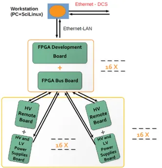
The new high voltage distribution card being developed by the Portuguese team, called HV Remote, aims to overcome some problems placing the HV Remote cards in a room 100 m away from the detector cave, designated by USA15 (low radiation environment). This will avoid the exposure to radiation, expanding the lifetime of the system and allowing for immediate maintenance and replacement when needed, overcoming two of the major problems of the actual system. In this case the high voltage distribution to PMTs is done with a cable. 256 HV Remote cards will be produced, each one will be able to supply 48 PMTs (having 48 channels). Each channel will be controlled from a dedicated control system on the HV Remote board and by a digital control system implemented on a Field Programmable Gate Array (FPGA). Sixteen HV Remote plus power supply boards will be controlled by one FPGA board. Finally, the FPGA boards will be controlled by the digital control system (DCS), which is TileCal’s general control system, figure 1.3. But this system has one major disadvantage, which is that it requires a large number of multi-conductor cables.
The main goals that HV Remote aims to achieve are:
• Be able to turn on/off each channel of the PMTs individually;
• Individually adjust the high voltage supply value (between -360 V to -1000 V) for each PMT;
• Reading the high voltage value applied to each PMT; • Reading of two temperature sensors;
• Reading a test reference voltage;
• Revision of the individual PMT HV control loop to mitigate the noise.
Figure 1.3: HV remote system control architecture.
As in this new system will be implemented a digital control, as well as the associated buses, not existing in its predecessor, the dedicated HVMicro control card will no longer be required. It should be noted that in this new system instead of primary high voltage sources will be developed dedicated high and low voltage power supplies. These will be the central point of this thesis, where will be presented all the steps taken in the development of dedicated sources as well as current state of the project and the work that is yet to be done.
1.4
Proposed Power Supplies Board
As mentioned earlier, the purpose of HV Remote is to distribute high voltage to PMTs. These individual voltages are obtained from a high voltage that must initially be supplied to HV Re-mote. In the current HV distribution system (HV Opto), the low power supplies are shared with the other ATLAS detectors, this means that the low power supplies are in the cave near the detector and a primary HV source is placed in the USA15 room. With this new HV Remote system, all the needed power supplies, will have to be installed also at the USA15 room, near to the HV Remote board. On the other hand, to mitigate the HV noise, for economic reasons and to facilitate their maintenance/replacement, low power printed circuit board (PCB) mount DC/DC converters to HV are used, instead of an expensive primary HV source. Thus, there is a need to project a board capable of producing the necessary power supply voltages for the HV Remote, the high and the low voltages, and that was the main objective of this thesis.
The Power Supplies board will be a dedicated power supply card that will be connected to the HV Remote board, and there will be one Power Supplies board for each HV Remote, so it will have to meet some criteria so that when both are connected they can work properly:
• The board must be capable of providing high voltage, with low noise, and be able to produce two alternative HV values, −830 V and −950 V both with 10 mA of output current, so each PMT can receive the necessary supply to work in perfect conditions;
• It has to provide the following low voltages: ±12 V with 2.5 A of output current, and 3.3 V with 0.8 A of output current, to the analog and digital components of the HV Remote board;
• It shall be able to read and send to the FPGA (that resends to the DCS system) the power consumption of each power supply (current and tension);
• It should allow the temperature reading on 2 different places of the board;
• It must offer the possibility of turning off the power supplies individually by software (digital control system) and turn them off all together by hardware (manual switch).
This thesis will feature a more detailed description of the mentioned supply board, called Power Supplies board, of the interface that will be used with the board which allows the digital control system and the board tests that were made. Namely, to some of the used components and to ensure that it will work properly. The Power Supplies board will use the same protocol as the HV Remote board, as illustrated in figure 1.4, although it will be used a serial peripheral interface (SPI) bus independent from the one of the HV Remote board.
Figure 1.4: Diagram of HV Remote distribution system and dedicated power supply card.
The following chapters will describe in detail the Power Supplies board design process (Chap-ter 2) and how it works, followed by a description of the user in(Chap-terface that will control the Power Supplies board (Chapter 3). In chapter 4 a description of the tests that will have to be performed in order to ensure its proper functioning will be presented, culminating with the conclusions drawn from the work done and work to be done in the future (Chapter 5).
Chapter 2
Power Supplies Board
As already mentioned in the section 1.4, the purpose of this thesis was to develop the Power Supplies board for the HV Remote. This chapter will detail the main features, as well as, the development steps of this board.
Figure 2.1: Power Supplies board scheme.
This board has to deliver all the voltages necessary to the HV Remote, with low noise. In the case of high voltages, need to be capable of producing two high voltage values, −830 V and −950 V @ 10 mA, because each PMT in TileCal is unique and during operation may behave differently. To properly calibrate the PMTs voltage, one of these two values need to be supplied to the HV Remote. The other voltages this board must supply are low voltage, ±12 V @ 2.5 A and 3.3 V @ 0.8 A, for the analog and digital components of the HV Remote board. The Power Supplies board should be able to read the current and tension consumptions of the board. In order to be able to supply all the necessary voltages for the HV Remote, the Power Supplies board uses dedicated DC/DC converters, which convert the incoming voltage from 2 external 24 V @ 20 A sources to the desired power supply, as shown in figure 2.1. Each crate will be powered by 2 of these external 24 V @ 20 A sources, ie each 2 external sources will supply 32 boards since each crate will have 16 HV Remote boards plus 16 Power Supplies boards (figure 1.3).
To control the output voltage of each of the two HV supplies an appropriate digital signal must be send by the digital control system. This system is based in a SPI communication protocol and to separate the received serial data, a serial to parallel converter is needed. For that, a 16-bit port expander with SPI interface (MCP23S17) is used, this expander also controls the enable/disable of each DC/DC converter used to obtain the desired power supplies. In this board was also implemented a 16-bit analog multiplexer (MPC506) which is used together with a 12-bit ADC (MAX1240) to provide all consumptions as well as the output of two temperature sensors (TMP17), placed in two different positions, thus allowing a temperature flow monitoring.
2.1
Project
The first step in the development of the Power Supplies board was the project of all the circuits needed to fully fit all the board requirements. This is the most interesting part of the project. Not less important is the choice of the components (in Appendix B is presented the list of all used components), as this choice must respect certain parameters so that the Power Supplies board can perform the required features. One of the biggest problems in this step was the appropriate choice of DC/DC converters, since we can only use, for each set of 16 Power Supplies boards: two 24 V @ 20 A, one 3.3 V @ 0.8 A and one ±12 @ 2.5 A power supplies. The 24 V @ 20 A power supplies are the primary power sources from which all others (the output power sources to HV Remote) are generated, being all DC/DC converters powered by these two power supplies. The input 3.3 V @ 0.8 A and ±12 @ 2.5 A power supplies will be in charge of power all other components used on this board. Thus, we have a limitation of current that we can use versus the current that is required to be supplied to the HV Remote board.
In the first approach to the choice of components this problem was quite evident. The choice of DC/DC converters at an early stage had only counted the current required for the normal operation of board with all PMTs on and not for the case as they are off as required (in the worst case all the 48 PMTs are off). When a PMT is disabled, due to the implemented circuit in HV Remote, the current consumption increases. To solve this problem, new DC/DC converters had to be chosen but this time taking into account what the two 24 V @ 20 A are supplying in relation to the consumption of the Power Supplies board converters, not forgetting that the current supplied by the converters has to take into account the current consumption of the HV Remote board. A new choice of the two external power supplies (24 V) need also to be done, taking into account the fact that they are common to all the boards the crate and they supply 16 Power Supplies boards and not just one.
For each Power Supplies board, four DC/DC converters were chosen, two of them generate the primary HV, −830 V and −950 V @ 10 mA, (C12446-12 Hamamatsu), one for the HV Remote digital circuits, 3.3 V @ 0.8 A (TDK-Lambda CC1R5-2403SF-E), and other for the HV Remote analog circuits, ±12 V @ 2.5 A (TDK-Lambda CCG304812D). It is necessary to use 2 HV DC/DC converters to increase the stability and to ensure that all PMTs get enough current. Another concern at this stage was the need for the voltages produced by the DC/DC converters to be as stable and low noise as possible. Therefore, there must be a careful choice
latter require close attention to their PCB placement and should be as close as possible to the respective power supplies input pin.
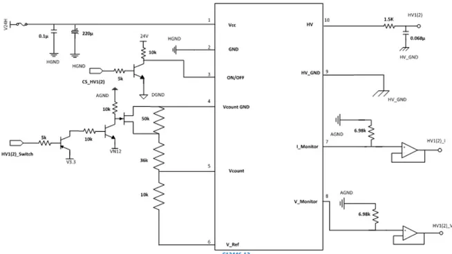
Figure 2.2: Electrical scheme of the electronics associated with the DC/DC converter (C12446-12 Hamamatsu 0 V to −1000 V @ 10 mA).
In the case of the HV converter, figure 2.2, it was necessary to use some components to select the voltage that the converter would be outputing, since this converter offers the ability to produce voltages between 0 and −1000 V. To do this, we first looked at its data sheet [13], the manufacturer recommended two different circuits to do so. The first was using an external voltage setting an output voltage value, the second circuit made use of a potentiometer to regulate the output voltage, as represented in figure 2.3. Both circuits were unsuitable for what was intended but the first was not useful as it did not allow changing by software the output voltage and the HV Remote needs 2 different HV voltage values. The second was not convenient either because although it allows changing the output voltage it could only be changed manually. In order to be able to change the voltage by user in the DCS system, it was required to create a new circuit that would allow this. This circuit is shown on figure 2.4, and uses two bipolar junction transistors, BJT, one PNP (BC559BTA) and one NPN (BC549B), one Junction Field Effect Transistor, JFET, N-Channel Switch (J111) and a resistors chain. The transistors change state, cut-off or saturation, are depending on a digital signal sent by the DCS. When the JFET is in cut state −950 V output (signals HV1 Switch and HV2 Switch for each HV output, table 3.1, with low) and when it is in saturation state −830 V output (signals HV1 Switch and HV2 Switch with high).
(a) Output voltage control by external voltage, using pins 4 and 5 from the converter[13].
(b) Output voltage control by external po-tentiometer, using pins 4, 5 and 6 from the converter[13].
Figure 2.3: Circuits recommended by the manufacturer to select the output voltage of HV con-verters.
The implemented circuits associated to the low voltage DC/DC converters are shown in fig-ures 2.5 and 2.6. Some of these circuits, as the filters, are recommended by manufacturer but others are needed to full fit the specific requirements of DCS, to ensure that it would be able to do the enable/disable of the converters and made the real time reading of consumptions. A more detailed description of this circuits is made in 2.1.1 and 2.1.2.
Another required feature is the temperature reading into different places (2.1.3) of the Power Supplies board. These measurements are important to know the temperature flux in operation and to design a proper cooling system.
Figure 2.5: Electrical scheme of the electronics associated with the DC/DC converter (TDK-Lambda CC1R5-2403SF-E 3.3 V @ 0.8 A).
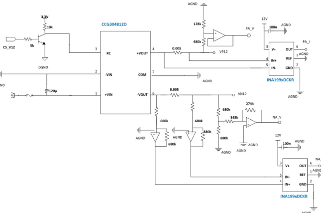
Figure 2.6: Electrical scheme of the electronics associated with the DC/DC converter (TDK-Lambda CCG304812D ±12 V @ 2.5 A).
The second step of this project consisted in the design of the Power Supplies board PCB, to do so it was used the program called Altium Designer 16.0 from Altium Limited. This step will de developed in 2.2.
2.1.1 Enable/Disable of the DC/DC Converters
In the Power Supplies board each DC/DC converter can be enabled/disabled in two different ways, one strictly digital and its command can be remotely executed via computer (DCS), and another manual that allows to turn off all the converters at the same time with a hardware switch implemented as a safety issue and for board maintenance/substitution.
The digital enable/disable uses one of the pins of each converter, specific for this task. This pin is connected a general purpose transistor with junction NPN (2N3904) and two resistors, one of 5 kΩ and one of 10 kΩ, in the base and in the collector respectively. It’s possible to see this circuit connected with pin 3, called on/off, in figure 2.2. In figure 2.5 the referred circuit is connected with pin 2, called RC, and in figure 2.6 it’s connected with pin 3, also called RC.
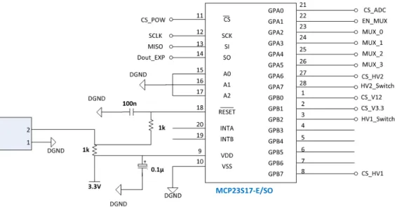
To control the state of each converter the output values of the 16-bit port expander with SPI interface (MCP23S17) are used, figure 2.7. This component communicates directly with the computer through the SPI communication protocol. This protocol allows sending a command to the port expander, using the Graphical User Interface (GUI), which was developed in this thesis specifically for the Power Supplies board, to activate the converters. In the output registers of the port expander a low or high digital signal (CS HV1, CS HV2, CS V12, CS V3.3, figure 2.7) are connected to the resistors at the base of transistors 2N3904, causing them to change state. As an example, when a low digital signal is sent the transistor will be in cut-off state, which means that in the pin RC of the DC/DC converter is applied a voltage of 3.3 V, then the converter will be activated, and deactivated when the digital signal sent is high, figure 2.5. In the case of the HV converter the activation method is similar with only a difference in the voltage applied to the collector resistor, since to activate this one a 2.4 mA current is required which is obtained by applying 24 V instead of 3.3 V, figure 2.2.
Note that during component testing and the development of the GUI, instead of the FPGA, a Raspberry Pi 3 B+ card was used, in conjunction with a code specially developed for this project, which will be presented in Chapter 3.
As you can see in the figure 2.7, the output signals of the port expander also controls the output voltages of HV converters, as well as the multiplexer and the ADC components. This will be further explained in section 3.2 where the code developed for the GUI will be presented.
The other way to disable the converters (an hardware one) is to cut off the voltage supply to the Power Supply board, thus disabling not only the converters but all other components that need an external voltage to work. This is done by placing three switches, U18, U19 and IC4 represented in figure 2.8, just after the socket where the voltage supplies are provided by
Figure 2.7: Electrical scheme of the electronics associated with the 16-bit port expander with SPI interface - MCP23S17.
that are used to power this board, two 24 V @ 20 A, one 3.3 V @ 0.8 A and one ±12 V @ 2.5 A, noticing that the last one have two different tension values that can be provide at the same time thus counting as 2 different power supplies. It’s used a switch for the two of 24 V (ADG5421BRMZ-RL7), other for the ±12 V (ADG5421BRMZ-RL7) and other to the 3.3 V (ADG601BRTZ-REEL7), as seen in the figures 2.8a, 2.8b, 2.8c respectively. After that, the control pins of the three switches are connected to one of the pins of a connector of 3 pins, that is displayed in figure 2.8b designated as P2 (Header 3). The other 2 pins of this connector are wired, one to the ground (0 V) and the other to the 3.3 V external source. This connector (P2, figure 2.8b) will be substituted by an analog switch, when the board is produced.
Figure 2.8d shows the schematic of the ADG601BRTZ-REEL7 switch, and through this it is possible to see that the operation of this type of components is not very complex, having only 3 pins, besides the power supply, one of them being pin D where a signal is input, pin S where the signal goes out if pin D is connected to S and pin IN which controls whether the two previous pins are connected or not. The ADG5421BRMZ-RL7 switch works the same way as ADG601BRTZ-REEL7 with the only difference being that the circuit is duplicated allowing two signals to be input and output at the same time.
As already mentioned, the P2 connector will then be replaced by a manual switch, which will allow to disable all converters at the same time, this is done by breaking the connection between the Power Supply board and external power supplies. This substitution is shown in figure 2.9, and in this case, when the manual switch is in the off position a digital signal will be sent to all IN pins of the three switches (U18, U19 and IC4), breaking the connection between pins D and S, thus disrupting power to the Power Supply board, which will only be restored when the position of the manual switch changes to on.
(a) Low voltage external power supply (24 V @ 20 A) switch (ADG5421BRMZ-RL7).
(b) Low voltage external power supply (±12 V @ 2.5A) switch (ADG5421BRMZ-RL7).
(c) Low voltage external power supply (3.3 V @ 0.8 A) switch (ADG601BRTZ-REEL7).
(d) Schematic figure of the switches.
Figure 2.8: Switches used to turn off sources in case or digital mode does not work.
2.1.2 Real-Time Consumption Readings
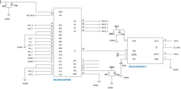
Real-time DC/DC converters consumption readings, both current and voltage, are taken us-ing a 16-bit analog multiplexer (MUX36S16) and a 12-bit ADC (MAX1240), both represented in figure 2.11. The last one is connected to the MISO1 Serial Peripheral Interface (SPI) sig-nal, which is read by Raspberry board to the GUI that will run on a computer, transmitting the information to the user. However, not all converters used have a pin that provides this infor-mation, as is the case with 3.3 V and ±12 V converters, CC1R5-2403SF-E in figure 2.5 and CCG304812D in figure 2.6 respectively, so it is necessary to implement other components to make this possible.
The HV converters are the only ones that have output pins that allow reading current and voltage consumption directly. Since these pins provide voltages between 0 and 5 V depending on the current and voltage the converter has on the output, it is also necessary to perform a conversion of these values to obtain the actual consumption, which is given by 0.5 mV / V for voltage and 0.5 V / mA for current. However, due to the limitations of the analog multiplexer, the maximum input voltage is 2.5 V, it is not possible to use the values directly from HV converters. This limitation is easily overcome by using a passive linear circuit that produces an output voltage that is a fraction of its input voltage, is called a voltage divider, and the simplest way to implement this circuit is to use two resistors in series, figure 2.2.
In figure 2.10a it’s represented the referred voltage divider, and the output tension is calcu-lated by the equation 2.1, were Voutis the output voltage and Vinis the input voltage.
Vout =
R2
R1 + R2 × Vin (2.1)
As in this case it is only necessary that the maximum reading output of the reading pins is 2.5 V and since these pins have an output impedance of 10 kΩ, a resistor close to this value is used. In addition to that is also used a buffer, figure 2.10b, so that there is no influence of the input impedance of the multiplexer, which could cause an error in the division of voltage giving at the end a wrong value. In fact, a smaller resistor is used (6.98 kΩ), as shown in figure 2.2 in pins 7 and 8, because the maximum output that is taken from this converter is -930 V and this is not the maximum this converter can provide, thus the equation 2.1 would look like:
Vout =
6980Ω
10000Ω + 6980Ω× Vin (2.2)
For the others, there were some differences to obtain the consumption values. Since this reading pin does not exist, the voltage output pin was used directly. For the ±12 V DC/DC converter, special attention must be paid to the fact that it has two different outputs, one positive and one negative, which implies that the way each reading is made is different, since the multiplexer only accepts positive values. Therefore, a voltage divider is also used in this output but instead of the buffer an inverter voltage amplifier circuit, figure 2.10c, is used to invert the signal so it can then be supplied to the multiplexer.
1
(a) Voltage divider scheme [14].
(b) Buffer scheme [15].
(c) Inverter voltage amplifier circuit scheme [16].
(d) Current sense amplifier ina199 [17].
Vout =
−R3
R4 × Vin (2.3)
In the equation 2.3, it can be seen that this circuit may have a voltage gain of less than one, making the voltage divider circuit unnecessary at first glance, but this is not quite true. As mentioned above, because there is a very tight margin in relation to the voltage that is produced by the converter and the one that needs to be supplied, it is imperative to avoid losses. As the readings of the consumptions are being taken directly at the output pin of the converters, there will be a loss of current, however it can be minimized using resistors with a high impedance, which is why voltage divider are used, not only to reduce voltage but also to prevent current losses, as possible to see in figure 2.6 in the pin 6.
To read the current consumptions it is not necessary to use a voltage divider or a buffer as referred to the voltage readings, but it is still necessary to use an inverter voltage amplifier circuit in the negative output, we need to use a special type of resistors to mitigate the output voltage loss, current sense resistors, which are used to monitor the current in a circuit and translate the amount of current in that circuit into voltage that can easily measured and monitored. But because of the small value of the resistor (0.005 Ω), the voltage drop is too small so, a dedicated amplifier is needed, a current sense amplifier (or current shunt amplifier, figure 2.10d). These special differential amplifiers give an output voltage proportional to the current flowing in sense resistor. The current sense resistor value used is 0.005 Ω and the current sense amplifier gain is 200, so the current value is given by the equation 2.4, where ∆V is the output voltage of the current sense amplifier.
I = ∆V
0.005 × 200 (2.4)
For the 3.3 V converter, as for the ±12 V converter, a voltage divider and a buffer are used to read the voltage consumption, and a current sense resistor is used to read the current consumption along with a current sense amplifier, where the values of these two last ones are the same ones used in the ±12 V converter, meaning that the current it’s obtained using the equation 2.4 as well.
It is important to note that because only one ADC is used, only one value can be read at a time, this value being in this case the output value of the multiplexer. The description of the read values is defined in table 3.4 and the value read is defined by the user. This will be further explored in Chapter 3, where the definition of these readings as well as the multiplexer channel to which they are assigned will be relevant for GUI development.
2.1.3 Temperature Reading
As mentioned earlier, two 24 V power supplies, which are used to power all DC/DC converters (one for HV converters and the other for low voltage converters), have a current of 20 A, and due to this factor there may be overheating in the components that are supplied by them. However, it is not the only source of heat, all the components in operation release heat and
Figure 2.11: Electrical scheme of the electronics associated with the 16-bit analog multiplexer MUX36S16 and the 12-bit ADC MAX1240.
once the board is finished and implemented in a crate, it will be surrounded by many other boards. Although they may not produce much heat on their own, when together this heat can be greatly increased. Because of this the temperature reading at two different points on the board is very important, although it is not very relevant at the prototype stage this board is in, as only one board will be used. Reading the temperature at two different points on the board will provide information on the temperature flow and type of cooling system that will need to be implemented in the crate to prevent component overheating, resulting in malfunction or even total breakdown of the Power Supply boards.
For this, two monolithic integrated circuit temperature transducer, TMP17, were used, figure 2.12. This circuit provides an output current that is proportional to absolute temperature. The output of the TMP17 is converted in a voltage and is one of the multiplexer analog inputs. In the figure 2.13 the graph of the transfer characteristics of the TMP17 is represented. It is through this that it is possible to obtain the temperature value from the signal send by the ADC, presented at last in GUI.
Figure 2.12: Electrical scheme of the electronics associated with the temperature transducer, TMP17.
Figure 2.13: Transfer characteristics of TMP17 [18].
2.2
Printed Circuit Board
After the schematic designs are completed (presented in Appendix A), the next step is the printed circuit board (PCB) design. It is at this stage that all circuits, presented in the schematic designs, are translated into an actual physical design. But when it comes to designing high volt-age PCBs, it’s important to ensure that a good layout can optimize the strengths of the electric field to optimize the operation and lifetime of the PCB. Although the process of manufacturing high voltage PCBs does not differ greatly from that of normal PCBs, more careful attention to the materials used and their properties are critical to success. A thorough understanding of spacing rules, clearances, operating frequencies, and design techniques will greatly help you avoid setbacks and potential challenges, and there are some things that need special attention, such as [19]:
• Isolating high voltage areas - it’s very important to group the high voltage circuitry together in order to minimize the impact that it will have on the rest of the board, and by doing this it’s possible decrease the risk of arcing on the board [19];
• Decreasing voltage across the board gradually - even if isolation is done, by doing this, the roughness of the entire board is increased, preventing potential problems that could arise even with isolation [19];
• Isolating noise sources - if this is not done the noise can couple through parasitic capaci-tance on the board or in the insulation, this will allow an easy propagation to areas of the board that are very sensitive, compromising its integrity [19];
• Minimizing interconnects - if fewer interconnects are used, the odds of happen transient generation in the design are reduced, if not, it can damage sensitive components or reduce the performance of the board. This will also minimize the propagation of high voltage across the board. Special attention must be taken in the connections between
Figure 2.14: 2D printed circuit board of the Power Supplies board.
components and its noise decoupling capacitors. Some of them should be placed in the bottom side of the board to achieve that [19].
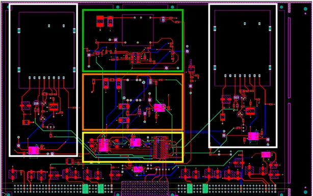
Figure 2.14 shows the final appearance of the PCB in the Altium environment. Within the white rectangles is the area of the board that is dedicated to the high voltage, isolated from the others, in the green and orange rectangles is the ±12 V DC/DC converter and the 3.3 V DC/DC converter, respectively, as well as all the circuits associated with them, and finally inside the yellow rectangle are the digital circuits, thus being separated from the analog ones. The figure 2.15 shows the same PCB but it is in 3D. The board consists of 8 layers, as shown in figure 2.16, of which 3 are mass planes, 1 an output power plane, 1 an input power plane and 1 a layer for signals. There are only components in the top layer and bottom layer, the others are internal layers. But this is just the end product, before the PCB looked like this there was a lot of work invested along the steps required to design a good performance PCB. The first thing to do when starting to design the PCB is the placement of components, this is a very important step as it affects all future work, so it has to be done carefully and is a lengthy process.
Figure 2.16: Layer stack of the Power Supplies board.
During the placement phase, there are some things that need to be present in the mind of the person performing this process. For instance, it’s necessary to think about manufacturing, this means that several considerations must be taken into account during the design. The first is component orientation, if all components are always facing the same direction, when the board is produced, installation, testing and inspection will be much easier [20].
The second point to consider is how components are placed relative to each other. When the board is complete and ready for manufacturing, it will go through a solder oven to connect all parts to the empty circuit board. If big components block the small ones, they are likely to be poorly soldered. Another aspect that can be very crucial, and in the case of power supplies is very important, is when placing the components, always pay attention to size, not only in two-dimensional space, but also the height, width and weight, as is the case with HV converters that have to be placed at each end of the board so that there is no overweight on one side which can cause a break in the board [20].
Another thing to keep in mind during this step is to think about routing, although we are not in this step yet, it is important to take this into account so as not to make the mistake of placing components too close, causing a lack of space when routing starts, or the fact that if the components are too close this may heat up more [20]. Attention should also be paid to signal induction, which may be caused by the proximity of the components, as well as extra caution in separating the digital from the analog, since if they mix together the board will not work as intended. Finally, it is very relevant to have good mass planes as well as power plans, since they allow a great attenuation of the fluctuation of the voltages that may exist in both planes, thus allowing a noise reduction that is crucial in this project.
After these was taken into consideration, the placement was made, the HV converters were placed at the end of the board, one on the right and one on the left, and underneath were all the components associated with filters and consumption measurements, no others components were placed in these two areas, isolating the high voltage from the others components. The port expander, the multiplexer and the ADC, as these must communicate with all DC/DC converters, need to be in the middle so that the path through which the information travels is similar. They have been placed on the bottom of the card in the central zone near to the connector dedicated solely to signals such as the used SPI signal (MOSI2, MISO3 and SCLK4) and the chip select
signal of the board. This region deals with all the digital circuitry of the Power Supplies board. The 3.3 V and ±12 V converters were placed on the top of the board in the central area, so that they did not interfere with the other components, along with all components associated with the filters and its consumptions readings circuitry.
One very important thing I learned from doing this thesis was that when we are placing the noise decoupling capacitors on the PCB, we want them to be as close as possible to their re-spective components. One of the most effective methods to do this is to put the components on the top layer of the PCB and the capacitors immediately below them on the bottom layer con-necting them with a via. This method saves a great deal of space and greatly reduces the noise that could be introduced by the distance between the components and their recommended ca-pacitors, which could be quite critical for this board since one of the requirements is to be able to produce low noise voltages.
2Master Output Slave Input - data output from master 3
Master Input Slave Output - data output from slave
After placement is completed, the next step is routing. In this step, the worst thing that can happen is to connect the networks incorrectly, but with the help of the Altium designer program this is not likely to happen. The other concerns at this stage are the crossing between nets and the width of the nets, the latter being quite relevant in this board, since there are high currents running through the nets and if the width is not adequate it will cause nets to overheat and consequently their rupture. In figures 2.17 and 2.18 are represented a table and a graphic of the trace width versus the current carrying capacity of a net that was taken in account during the routing process, it is important to note that in these figures the net used is only 1 oz. of thickness.
Figure 2.17: PCB trace width vs. current carrying capacity table [21].
Figure 2.18: PCB trace width vs. current carrying capacity graphic in different temperatures [21].
The first thing to do in the beginning of PCB design, was the creation of the 3 mass planes, one for high voltage, HV ground, one for analog voltage, analog ground, and another for digital voltage. These are isolated from each other except for a single point where the three are connect. By doing this in the first place it is possible to simplify the connections that have to be made because the ground line connections of each component disappear (as these are made directly), and the fact that we have three separate planes in different layers allows us to have a very stable mass planes which reduces noise produced by the currents return.
Following the same principle of stability and low noise, polygons were used to make the supply and output voltages net planes, by doing this the voltages become more stable and are not affected as much by noise, as well as avoiding the problem of nets width. But there has to be extra care for the high voltage plane that is made using an exception to define the minimum clearance allowed between any two primitive objects on a copper layer, this allows a good isolation of the HV net with every other nets. In Appendix C it’s possible to see the routing done by layer, however the mass planes are not represented since there are no nets in these layers.
After this is done, only the nets that connect the components to each other and the nets of the control signals remain, and to do this routing, there are 3 different layers, namely the top, the bottom and an internal signal layer. In the end, all the project properties were validated with the help of the Altium designer program, and all errors were corrected. After that a bill of material was also generated through the Altium designer program (presented on Appendix B), as well as a file of board plans and perforations and one of the position of the components. All of that are also done by the Altium designer program and a set of layer planes, called the gerber files, with all the information need are generated. These are files needed to the PCB fabrication. Only after this is complete is the board finally ready to be shipped for fabrication. Right now the Power Supplies board is in fabrication in one of the two different companies, the first is EUROCIRCUITS that is in charge of manufacturing the board without the components, and to do so they need the file of board plans and perforations previously generated. The other is Systion Electronics Lda, that is in charge of the assembly of the components, so they need the board already manufactured as well as the information of where to place the components, that can be found in the file of the position of the components.
Chapter 3
User Interface and Communication
with Power Supplies board
In this chapter a detailed description will be given of the graphical user interface developed to facilitate communication between the Power Supplies board and the user, as well as how communication between them is performed. In figure 3.1 we can see the block diagram of the Power Supplies board digital control. The control master is a PC/workstation configured as a node of the DCS (Detector Control System) of ATLAS. The DCS will use an interface specifically created for this board, developed in WinCC programming language, in order to facilitate the communications that occur between the DCS and the Power Supplies board, which takes place with an FPGA as an intermediate. The DCS will control the port expander, and the outputs registers of the port expander will be connected to the multiplexer, the ADC and to the enable/disable pins of each DC/DC converter, allowing its digital control. The multiplexer was used to permit to read the analog signals from two temperature sensors, current and voltage consumptions of the DC/DC converters, one at a time. It’s output value, with the value selected by the user, is the input signal of a 12-bit ADC that will convert these signals into digital ones.
![Figure 1.1: TileCal hadronic calorimeter structure [5].](https://thumb-eu.123doks.com/thumbv2/123dok_br/19288642.990670/18.892.277.615.571.845/figure-tilecal-hadronic-calorimeter-structure.webp)


![Figure 2.13: Transfer characteristics of TMP17 [18].](https://thumb-eu.123doks.com/thumbv2/123dok_br/19288642.990670/36.892.257.637.125.436/figure-transfer-characteristics-of-tmp.webp)