608 Brazilian Journal of Physics, vol. 34, no. 2B, June, 2004
Initial Growth of GaN and InN Over GaAs (110) Substrates
A. de Paiva, J. L. A. Alves, and H. W. Leite Alves
Departamento de Ciˆencias Naturais, Universidade Federal de S˜ao Jo˜ao del Rei Caixa Postal 110, 36.300-000, S˜ao Jo˜ao del Rei, MG, Brazil
Received on 31 March, 2003
We present, a systematic theoretical study of the adsorption of Ga, In and N over GaAs (110) surfaces based on parameter-free, self-consistent total energy and force calculations using the density functional theory. We analyzed the changes in the bond-lengths and in the bond-angles before and after deposition, as well as the total energy behaviour with the adsorbate chemical potential variation. Our results show that the GaN growth over GaAs (110) is energetically more favorable than the InN growth. However, the resulting InN film can be cubic only if we apply small strains on the substrate, while the GaN one is hexagonal.
1
Introduction
The group III-nitrides(AlN, GaN, InN) and the correspond-ing alloys have attracted great interest due to their succesful applications in the electronic and optoelectronic device tech-nology [1]. However, their growth in the zincblende struc-ture has been a hard task to the experimentalists, once the most stable structure for these compounds is the wurtzite one.
To solve this interesting puzzle, a lot of substrates has been proposed for the III-nitride growth nitride growth in the cubic modification, and the nitridation of the GaAs sur-faces seems to be the most efficient method for such growth [2-4].
In order to understand the physical mechanisms of this new growth technique, we present, in this work, a system-atic theoretical study of the adsorption of Ga, In and N over GaAs (110) surfaces based on the density functional theory, the local-density approximation for the exchange-correlation term, within the plane-wave pseudopotential method (abinit code [5]). We have used the Hartwigsen-Goedecker-Hutter ultrasoft pseudopotentials [6]. The sur-faces were described by slab supercells build up of 7 atomic layers and a vacuum region equivalent of 5 atomic layers. Also, a (4 4 2) Monkhorst-Pack set ofk-points was used to sample the slab Brillouin zone [7]. Details about the conver-gence of the equilibrium bulk properties of GaAs, as well as the relaxed GaAs (110) surface properties were described in our previous work [8].
2
N adsorption
In Fig. 2, we show the variation of the total energy of the slab as a function of the height ∆z(in ˚A) of the N atom(referenced to to uppermost As atom) over the GaAs (110) surface, at the sites defined in Fig. 1 (the drawn lines
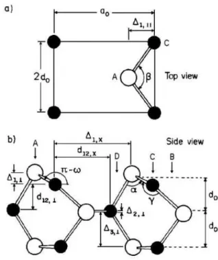
Figure 1. Atomic geometry of the GaAs (110) surfaces. (a) Top view of the surface unit cell. (b) Side view of the first three layers of the (110) surface. Open circles are anions and the shaded ones are cations. a0 is the lattice parameter,d0 =√2(a0/4), and the
letters A, B, C, D indicate the possible N adsorption sites.
A. de Paivaet al. 609
[4]. For the Ga and In adsorptions, we found the same fea-tures, and the calculated adsorption energies are 303 and 389 meV/atom, respectively.
It is interesting to note, from Fig. 2, that the stable posi-tion the adsorbed N atom will be 0.25 ˚A below the As sur-face atom. Based on this fact, we, then, have simulated the surface relaxation with the adsorbed N atom at the B site, and the final result is depicted in Fig. 3.
Figure 2. Variation of the total energy of the slab supercell as a function of the height∆z (in ˚A) of the N atom over the GaAs (110) surface at the sites A, B, C, and D, as defined in Fig. 1.
Figure 3. Relaxed atomic positions after the N adsorption at the GaAs (110) surface.
We can infer, from Fig. 3, that the presence of N atom pushes both the uppermost Ga and As atom back to the sur-face, creating an interesting metastable state: The N binds to both the uppermost Ga atom and the As in the sub-surface layer. At the same time, the N attracts the uppermost As atom, stretching the surface Ga-As bonds. As the N atom is more electronegative than As one and, as it arrives at the surface with sufficiently high energy due to the N plasma created in the nitridation, the adsorption process finishes by the break the surface Ga-As bonds, and the N atoms, then, can replace the surface As ones by a simple anion exchange. This should be the mechanism of the As mediated growth for GaN over GaAs substrates with a surfactant aspect [9].
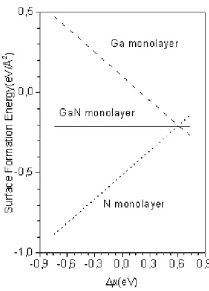
Figure 4. Surface formation energy,γ, of a N, Ga and GaN mono-layers over GaAs (110) surface, as a function of the difference of the chemical potentials of the monolayer constituents,∆µfor neu-tral charge states.
3
GaN and InN monolayer
adsorp-tion
We also simulated the adsorption of a monolayer of GaN, and of InN, over GaAs (110) surface. Our calculated re-sults for some structural parameters are depicted in Table I, compared with those of GaN and InN (110) surfaces [10]. First, we note that, in both cases, the uppermost layer(the GaN or InN monolayer) moves inward the surface, but it still keeps the fact that the cation relaxes inward and the an-ion outward [8]. Moreover, the final value for the tilt angle ωis less than that observed for the GaN and InN, and the GaAs layers does not relaxe too much from their original positions. Then, we can infer from our results, that the final GaN or InN thin films growth on GaAs (110) surfaces will not preserve the final (110) structure. The observed strains on the interface with the substrate suggest that, from Table I, the Nitride film structure changes toward a hexagonal one, as already observed experimentally [4]. However, if small strains are applied on the GaAs substrate, the InN film could be grown in a zincblende modification, because its lattice mismatch with the substrate is smaller than the GaN case.
610 Brazilian Journal of Physics, vol. 34, no. 2B, June, 2004
Table I. Calculated selected structural parameters for the GaAs/GaN and GaAs/InN (110) surface relaxations as defined in Fig. 1, compared with other theoretical results(the anglesωαandβare in degrees).
∆1,⊥( ˚A) ∆1,x( ˚A) ∆2,⊥( ˚A) ω α β
GaAs/GaN 0.002 4.905 0.13 0.21 103.7 104.9 GaAs/InN 0.140 4.682 0.12 9.6 101.6 111.5 GaN[10] 0.247 3.650 0.039 15.3 100.3 116.0 InN[10] 0.250 4.002 0.002 13.0 101.3 115.7
step for the initial growth of the III-Nitride, because the ad-sorption of a N monolayer is the most stable system, even at the Ga-rich conditions. The same picture is obtained for the InN growth. The main difference between GaN monolayer and the InN monolayer is the value of their surface forma-tion energy. While for the GaN monolayer, we foundγ = 213 meV/ ˚A2, for the InN one, we gotγ= 204 meV/ ˚A2, and
both systems are stable only at Ga-rich(In-rich) conditions. Finally, we presented our results of a systematic theo-retical study of the adsorption of Ga, In and N over GaAs (110) surfaces. Our results show that both the InN and GaN growth over GaAs (110) can take place, and the resulting Ni-tride film will have hexagonal crystalline symmetry. Also, the GaN growth is energetically more favorable than the InN growth. However, if we apply small strains on the substrate for the InN growth, we can get cubic samples. A complete description of our obtained results will be published soon elsewhere.
Acknowledgements
The computer resources were provided by the Centro Nacional de Processamento de Alto Desempenho em Minas Gerais & Regi˜ao Centro-Oeste (CENAPAD-MG/CO). A. de Paiva acknowledge the PIBIC-FAPEMIG/UFSJ program for the finantial support.
References
[1] S. C. Jain, M. Willander, J. Narayan, and R. van Overstraeten, J. Appl. Phys.87, 965 (2000).
[2] S. A. Ding, G. Neuhold, J. H. Weaver, P. H¨aberle, K. Horn, O. Brandt, H. Yang, and K. Ploog, J. Vac. Sci. Technol. A14, 819 (1996).
[3] P. Hill, D. I. Westwood, L. Haworth, J. Lu, and J. E. Mac-Donald, J. Vac. Sci. Technol. B15, 1133 (1997).
[4] D. Troost, H. –U. Baier, A. Berger, and W. M¨onch, Surf. Sci.
242, 324 (1991).
[5] X. Gonze, J.–M. Beuken, R. Caracas, F. Detraux, M. Fuchs, G.–M. Rignanese, L. Sindic, M. Verstraete, G. Zerah, F. Jol-let, M. Torrent, A. Roy, M. Mikami, Ph. Ghosez, J.–Y. Raty, and D. C. Allan, Comput. Mater. Sci.25, 478 (2002), and references therein.
[6] C. Hartwigsen, S. Goedecker, and J. Hutter, Phys. Rev. B58, 3641 (1998).
[7] H. J. Monkhorst and J. D. Pack, Phys. Rev. B13, 5188 (1976). [8] A. de Paiva, J. L. A. Alves, and H. W. Leite Alves, phys. stat.
sol. (c)0, 417 (2002), and references therein.
[9] H. Okumura, H. Hamaguchi, G. Feuillet, Y. Ishida, and S. Yoshida, Appl. Phys. Lett.72, 3056 (1998).
[10] H. W. Leite Alves, J. L. A. Alves, R. A. Nogueira, and J. R. Leite, Braz. J. Phys.29, 817 (1999).
[11] The surface formation energy,γ, was defined as:
γ= 1 2E
′
C− 1 2neµe−
1
4(NX−NN) ∆µ, whereE
′
Cis the
cohesion energy per surface area,neis the number of
elec-trons transferred from the electron reservoir (ne= 0, in our