ISSN 1517-7076 artigo 11551, pp.228-234, 2014
Autor Responsável: CRUZ, L. R. Data de envio: 26/02/2014 Data de aceite: 02/09/2014
Microstructural and optical properties
of CSS and CBD-CdS thin films
for photovoltaic solar cells
Leila Rosa Cruz1, José Antônio Sousa Fernandes1, Carlos Luiz Ferreira1, Wagner Anacleto Pinheiro1
1
Military Institute of Engineering, Materials and Mechanical Engineering Department, Praça General Tibúrcio, 80 – Urca, 2290-270 - Rio de Janeiro, RJ
e-mail: [email protected]; [email protected]; [email protected]; [email protected]
ABSTRACT
This work compares the properties of CdS films deposited by CBD and CSS techniques. The influence of the deposition parameters on the properties of the films was investigated. The thickness of CBD films ranged from 80 to 100nm and was affected by the concentration of reactants in the solution. For CSS films, the thickness was controlled in the 100-300nm range, being strongly influenced by the source/substrate tempera-tures and pressure. Grain size in CSS films was larger than in CBD films. Transmittance of CBD and CSS films ranged from 80 to 90%, but the band gap in CSS films was narrower than in CBD films, which means that CSS films transmit less of the blue part of the solar spectrum than CBD films. However, the growth of CdS films by CSS technique may be advantageous because the CdS/CdTe device could be fully manufac-tured in the same system.
Keywords: CdS thin films; CBD deposition; CSS deposition; microstructure; optical properties.
1. INTRODUCTION
229 2. EXPERIMETAL METHOD
CdS films were deposited by CBD and CSS onto borosilicate substrates covered with a bilayer of transparent conductive oxides: fluorine doped tin oxide/undoped tin oxide (SnO2:F/SnO2) – supplied by the National
Renewable Energy Laboratory (NREL).
CBD-CdS films were prepared by first immersing the abovementioned substrates in a beaker contain-ing 137.5ml of DI water heated at 90oC. Then, the reactants were introduced. Firstly, 2 ml of cadmium ace-tate [Cd(CH3COO)2], 0.033 M, and 1.2 ml of ammonium acetate (NH4CH3COO), 1.0 M, were added. The
cadmium acetate was the source of Cd and the ammonium acetate acted as a buffer solution, controlling the reaction rate. After 4 min, droplets of ammonia (3.7 M) were added very slowly in order to adjust the pH of the solution at 9. After that, 0.5 ml of thiourea [CS(NH2)2], 0.067 M, was introduced every 10 min up to a
total of 2 ml. The concentration of reactants in the solution was changed by doubling and tripling this volume of reactants, hereafter VR, while keeping constant the volume of water. The total deposition time, after the
addition of the first portion of thiourea, was 40 min. The substrates were then removed from the bath and rinsed in warm DI water.
CSS-CdS films were deposited in a homemade equipment composed of a quartz tube into which two graphite blocks, separated by a distance of 2 mm, were inserted to sustain the source and substrate. The graphite blocks, heated by halogen lamps, were used to homogenize the temperatures of the source and su b-strate. The CdS source was a 35m thick CdS layer deposited onto a borosilicate substrate. This source-plate was prepared by sublimating a CdS/propyleneglycol paste. Details about the equipment can be seen else-where [9]. The pressure of the system was varied between 5 and 15 Torr, using argon or a mixture of oxy-gen/argon.
Film thicknesses were measured in a Dektak 150 surface profiler from Veeco. X-ray diffraction (XRD) analyses were made on a Siemens D5000 diffractometer with a Cu anode. Grazing incidence mode was selected due to the small thickness of the films. The incidence angle was fixed at 1o and the scans were taken between 20° and 80° at 0.02° s-1. Optical transmittance spectra were obtained in a Cary 5000 spectro-photometer from Varian. Morphology was evaluated by atomic force microscopy (AFM) in a Veeco SPM DI3100 microscope.
Solar cells using CBD and CSS-CdS films were fabricated in the CSS system with the configuration glass/SnO2/CdS/CdTe/back-contact using the procedures described elsewhere [10]. Briefly, a 5-7 m thick
CdTe film was deposited onto glass/SnO2/CdS structures. The source and substrate temperatures for CdTe
deposition were 610 and 480oC, respectively, and the argon pressure was 1 Torr. The devices were finished according to the following procedures: the CdTe surface was submitted to a heat treatment in air (100 Torr), in the presence of a saturated CdCl2 solution, at 380 oC, for 30 min; after that, the CdTe surface was etched
with a nitric/phosphoric acid, and then gold was evaporated for the back contact. The efficiency was meas-ured in a system composed of a solar Simulator, model 81160-1000-1, from Oriel Instruments, a Xe/HgXe arc lamp (200-500 Watts), and a 3 A current source, model 2420, from Keithley.
3. RESULTS
Table 1 shows the thickness of CBD-CdS films deposited from solutions with different concentrations of reactants (the concentration increases with the volume of reactants, VR). As expected, the thickest film was
the one grown from the most concentrated solution, 3VR, since a larger number of Cd2+ and S2- ions was
available. It was found that this film had the proper thickness for manufacturing CdS/CdTe solar cells, which must be less than 100 nm [7].
230
Table 1: Thickness of CBD-CdS thin films as a function of the volume of reactants. VR = 2 ml of cadmium acetate, 1.2 ml of ammonium acetate, and 2 ml of thiourea.
SAMPLE VOLUME OF REACTANTS THICKNESS (nm)
1 1 VR 49
2 2 VR 58
3 3 VR 105
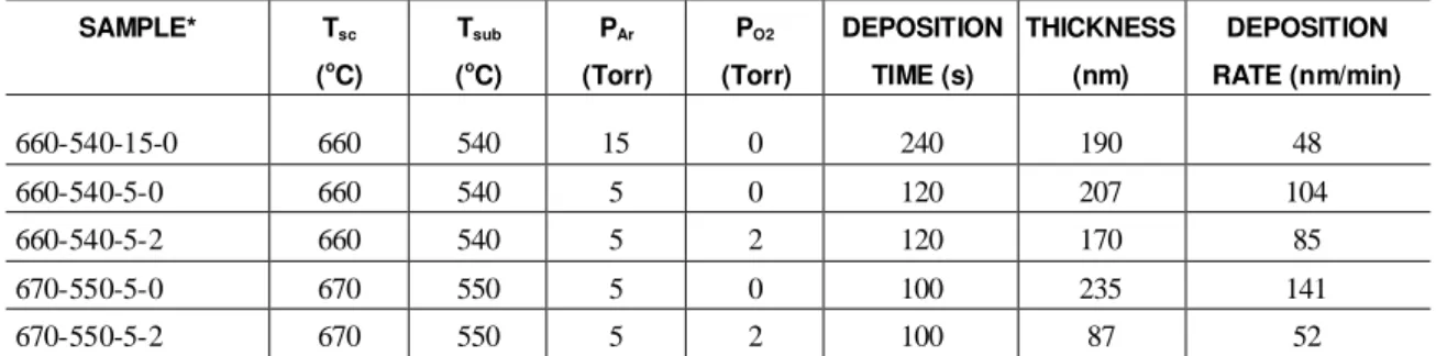
Table 2: Thickness and deposition rate of CSS-CdS thin films as a function of: source temperature (Tsc), substrate tem-perature (Tsub), argon pressure (PAr), and oxygen pressure (PO2). Source-substrate distance was 2 mm.
SAMPLE* Tsc (o
C)
Tsub (o
C)
PAr (Torr)
PO2 (Torr)
DEPOSITION TIME (s)
THICKNESS (nm)
DEPOSITION RATE (nm/min)
660-540-15-0 660 540 15 0 240 190 48
660-540-5-0 660 540 5 0 120 207 104
660-540-5-2 660 540 5 2 120 170 85
670-550-5-0 670 550 5 0 100 235 141
670-550-5-2 670 550 5 2 100 87 52
* The number describes the parameters used during the sample deposition (Tsc-Tsub-PAr-PO2)
Figure 1 shows AFM images of the surface of CBD-CdS films grown from solutions with different volume of reactants. The morphology in both films is quite similar, composed of agglomerates of nanograins. These agglomerates contributed to the surface roughness, which was evaluated by the root mean-square value (Rq), typically 8 nm, as given by AFM analyses. This is an acceptable value for the 100 nm-thick films. Fig-ure 2 shows AFM images of the surface of CSS-CdS films. The grains are bigger than in CBD-CdS films due to the higher deposition temperature. The morphology was strongly affected by the source/substrate tempera-tures, pressure, and presence of oxygen. The bigger grains in Fig. 2a were due to the lower deposition rate obtained for the films grown at higher pressures, as shown in Table 2. Figure 2c shows that the presence of oxygen in the gaseous mixture favored the growth of denser films with a better coverage, an important re-quirement for their application in heterojunction solar cells. The Rq roughness values ranged from 20 to 32 nm, as given by AFM analysis, and were greater than those found in CBD films due to the bigger grains in CSS films. It should also be noted that the roughness decreased when the films were deposited in the pres-ence of oxygen, certainly due to the denser microstructure. A similar result has been found in the literature for CdTe films [12].
231
Figure 1: AFM images of the surface of CBD-CdS films grown from solutions with different volumes of reactants:
a) VR; b) 3VR.
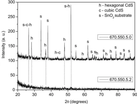
Grazing incidence diffractograms of CBD films are not shown here, as only a very low intensity (220) diffraction peak, from the CdS cubic phase, was hardly identified, confirming that the films were nano-crystalline. On the other hand, due to the higher deposition temperatures, most of the CSS-CdS films were crystalline, being predominantly composed of the hexagonal phase, as depicted in Fig. 3. It can also be ob-served that the presence of oxygen impaired the crystallinity of these films.
Figure 2:AFM images of the surface of CSS-CdS films grown at different conditions: a) 660-540-15-0; b) 670-550-5-0; c) 670-550-5-2
Figure 3:Grazing incidence x-ray diffraction of CSS-CdS films grown with oxygen (670-550-5-2) and without oxygen (670-550-5-0).
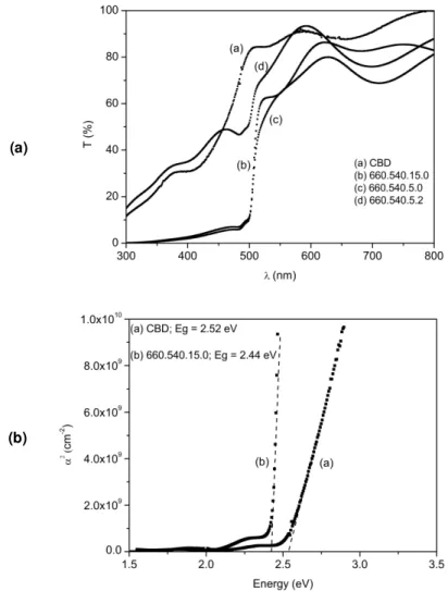
Transmittance of CdS films in the visible region ranged from 80 to 90%, for films deposited by both techniques, as can be seen by the spectra shown in Fig. 4a. It should be noted that the optical absorption edg-es were sharper in CSS films deposited without oxygen. Neglecting the reflectance at film/air and film/substrate interfaces, the absorption coefficient () of the CdS film at each wavelength () was obtained
232
from the transmittance data using Equation 1, where t is the thickness of the film, Ts is the transmittance of the substrate (glass/SnO2), and Tf,s is the transmittance of the film/substrate system.
(1)
The direct optical bandgap was obtained from the linear portion of the 2 versus photon energy plot [13], as depicted in Fig. 4b. The values – 2.52 eV (CBD films) and 2.44 eV (CSS films, mean value) – are close to those found in the literature [3-5]. The higher bandgap energy represents an advantage for CBD films, since absorption losses in the blue region may be minimized.
Figure 4: Optical properties of CBD and CSS-CdS films grown at different conditions: a) transmittance spectra; b)
ab-sorption coefficient versus photon energy for bandgap determination.
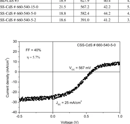
Table 3 shows photovoltaic parameters of the CdS/CdTe solar cells extracted from the current density (J) versus voltage (V) curves, as illustrated in Fig. 5. The results are a mean value of different areas of the same device, each one sizing roughly 0.5 cm2. The CBD and CSS-CdS films were deposited using the pa-rameters shown in Tables 1 and 2, respectively. The CdTe film and the completed cell were manufactured as described in the experimental method. The larger grain size, better crystallinity, and sharper absorption edges observed in CSS-CdS films did not imply in better devices. Indeed, the efficiencies () of CBD and CSS-CdS solar cells were quite similar, around 5%, except for the device CSS-CSS-CdS #
660-540-5-2
, which had its CdS film deposited under oxygen atmosphere. Although the literature reports that oxygen is beneficial to
s s f
T T
t
,
ln 1
233
the cell (usually, CBD cells – in which oxygen is naturally incorporated from the bath – are more efficient than CSS cells) [6], our results showed that it dramatically impaired the value of the open circuit voltage (Voc). This decrease in Voc suggests that the oxygen has led to the formation of oxides at CdS/CdTe inter-face instead of playing its role of increasing the cell efficiency. The mechanism by which oxygen improves the cell performance is not very well understood. Some authors propose that the properties of the films are affected by the reaction between the oxygen and the other species in the chamber, such as Cd, leading to the formation of cadmium oxide [12]. Such reaction changes the nucleation and growth kinetics of the CdS film, and hence its microstructure. Figure 2, which showed that a better coverage had been obtained when the CdS film was grown in an O2 atmosphere, confirms this proposition. The fill factor (FF) value of 40% was mainly
limited by series resistances originated mostly from the back contact that generated a rectifier barrier at Au/CdTe interface. The presence of this barrier was confirmed by the shape of the J x V curves in the first quadrant; it appeared as a saturation signal at voltages above Voc, a behavior commonly referred to as rollo-ver (see Fig. 5). Shunt resistances were identified in a less extent and may have been caused by shunt paths generated, for example, by discontinuities in the very thin CdS layer. For instance, the rough and o pen grained morphology of CSS-CdS films compared to the more compact one of CBD-CdS films may have con-tributed to the shunting characteristics of the J-V curves.
Table 3: Photovoltaic parameters of SnO2/CdS/CdTe solar cells: short circuit current density (Jsc); open circuit voltage (Voc); fill factor (FF); solar efficiency ().
CdS LAYER JSC
(mA.cm-2 )
VOC (mV)
FF (%)
(%)
CBD-CdS #3 18.9 627.9 40.4 4.8
CSS-CdS # 660-540-15-0 21.5 567.2 42.2 5.2
CSS-CdS # 660-540-5-0 18.8 582.4 44.2 4.8
CSS-CdS # 660-540-5-2 18.6 391.0 41.2 3.0
Figure 5: J x V curve of a CdS/CdTe solar cell.
4. CONCLUSION
234 5. ACKNOWLEDGMENTS
This work was supported by CENPES-PETROBRAS.
6. BIBLIOGRAPHY
[1] WALDAU, A. J., “Thin Film Photovoltaics: Markets and Industry”, Interna tional Journal of Photoener-gy, Review Article (2012), Article ID 768368, 6 pages. doi:10.1155/2012/768368.
[2] GREEN, M.A., EMERY, K., HISHIKAWA, Y., et al., “Solar Cells Efficiency Tables (version 42)”, Pro-gress in Photovolta ics: Resea rch and Applica tions, v. 21, pp. 827–837, 2013.
[3] MENDOZA-PEREZ, R., SANTANA-RODRIGUEZ, G., SASTRE-HERNANDEZ, J., et al., “Effects of thiourea concentration on CdS thin films grown by chemical bath deposition for CdTe solar cells”,Thin Solid Films, v. 480–481, pp. 173–176, 2005.
[4] WENYI, L., XUN, C., QIULONG, C., et al., “Influence of growth process on the structural, optical and electrical properties of CBD-CdS films”,Ma teria ls Letters, v. 59, pp. 1–5, 2005.
[5] MAHDI, M.A., HASSAN, Z., NG, S.S., et al., “Structural and optical properties of nanocrystalline CdS thin films prepared using microwave-assisted chemical bath deposition”, Thin Solid Films, v. 520, pp. 3477-3484, 2012.
[6] MOUTINHO, H.R., ALBIN, D., YAN, Y., et al., “Deposition and properties of CBD and CSS CdS thin films for solar cell application”,Thin Solid Films, v. 436, pp. 175–180, 2003.
[7] SCHAFFNER, J., FELDMEIER, E., SWIRSCHUK, A., et al., “Influence of substrate temperature, growth rate and TCO substrate on the properties of CSS deposited CdS thin films”, Thin Solid Films, v. 519, pp. 7556-7559, 2011.
[8] FELDMEIER, E.M., FUCHS, A., SCHAFFNER, J., et al., “Comparison between the structural, morpho-logical and optical properties of CdS layers prepared by Close Space Sublimation and RF magnetron
sputter-ing for CdTe solar cells”, Thin Solid Films, v.519, pp. 7596-7599, 2011.
[9] PINHEIRO, W.A., FALCÃO, V.D., CRUZ, L.R., et al., “Comparative Study of CdTe Sources Used for
Deposition of CdTe Thin Films by Close Spaced Sublimation Technique”,Ma teria ls Resea rch, v. 9, n.1, pp. 47-49, 2006.
[10] PINHEIRO, W.A., FERNANDES, J.A.S., CABOCLO, G.D., et al., “Fabrication of TCO/CdS/CdTe/Au solar cells using different CdCl2treatments”, In: Proceedings of the 33rd IEEE Photovolta ic Specia lists
Con-ference, pp.1-4, San Diego, CA, 2008.
[11] SOSA, V. CASTRO, R., PEÑA, J.L., “Pressure and temperature influence on CdTe thin-film deposited by close-spaced vapor transport technique”, Journa l of Va cuum Science a nd Technology, v. A8, n.2, pp. 979-983, 1990.
[12] CONTRERAS-PUENTE, G., VIGIL-GALÁN, O., VIDAL-LARRAMENDI, J., et al., “Influence of the
growth conditions in the properties of the CdTe thin films deposited by CSVT”, Thin Solid Films, v. 387, pp. 50-53, 2001.