Luís Filipe Galhofas Neto
Licenciado em Ciências de Engenharia Electrotécnica e de Computadores
Non-Gyrator Type Active Inductors
Dissertação para obtenção do Grau de Mestre em Engenharia Electrotécnica e de Computadores
Orientador: Prof. Doutor Luís Augusto Bica Gomes de Oliveira
Júri :
Presidente: Prof. Doutor Luís Filipe Figueira de Brito Palma Arguente: Prof. Doutor João Pedro Abreu de Oliveira Março, 2015
Copyright
Non-Gyrator Type Active Inductors
COPYRIGHT © Luís Filipe Galhofas Neto, Faculdade de Ciências e Tecnologia, Universidade Nova de Lisboa.
A Faculdade de Ciências e Tecnologia e a Universidade Nova de Lisboa têm o direito, perpétuo e sem limites geográficos, de arquivar e publicar esta dissertação através de exemplares impressos reproduzidos em papel ou de forma digital, ou por qualquer outro meio conhecido ou que venha a ser inventado, e de a divulgar através de repositórios científicos e de admitir a sua cópia e distribuição com objetivos educacionais ou de investigação, não comerciais, desde que seja dado crédito ao autor e editor.
“We grew up learning to cheer on the underdog because we see ourselves in them”- Shane Koyczan
Acknowledgments
Em primeiro lugar, quero expressar a minha enorme gratidão ao meu orientador, Professor Luís Oliveira, não apenas por me ter proporcionado a oportunidade de trabalhar neste tema, mas também pela total disponibilidade e amizade que sempre manifestou ao longo do curso para discutir as minhas dúvidas, acompanhadas de úteis observações e conselhos, que muito ajudaram na elaboração do presente trabalho e na conclusão do mestrado.
Um agradecimento aos meus colegas e amigos da Faculdade de Ciências e Tecnologia, por toda a camaradagem e ajuda prestada ao longo do curso.
Tornaram estes anos universitários valiosos e enriquecedores e tenho a certeza que o bem mais precioso e inestimável que levo da faculdade, para além do conhecimento adquirido, é a vossa amizade.
A este nível, gostaria de sublinhar o constante apoio que recebi dos meus colegas e amigos Ricardo Neves, Ali Saad e João Pires.
Agradeço também aos meus amigos de infância, das Paivas, do Fogueteiro, passando pelos tempos do Amora Futebol Clube, colegas e amigos da PT, Amorim Industrial Solutions, TMN, pelos momentos de lazer, mas também de constante incentivo.
Por último, gostaria de dedicar uma palavra especial de eterno agradecimento à minha família (sobretudo aos meus pais e meu irmão) por tudo o que tem feito por mim, motivando-me constantemente no sentido de ultrapassar todas as dificuldades, que foram muitas. Estou eternamente grato por todo o bem que me fizeram e o vosso amor incondicional.
Apoiaram-me em todos os momentos e decisões profissionais que tomei, e nunca deixaram de acreditar em mim.
Resumo
Receptores modernos de rádio frequência (RF) permitiram um eficiente e significativo crescimento de aplicações em CMOS.
O requisito principal consiste em ter o sistema num só chip, de maneira a optimizar área e o custo. Para o efeito, é necessário o desenvolvimento de circuitos sem bobines, para os blocos-chave de um receptor RF. Osciladores RC, filtros passa-banda RF, e LNAs são exemplos destes blocos-chave. A presente dissertação introduz um “inductorless wideband MOSFET-only RF Non-Gyrator Type of Active Inductors” com reduzida área de consumo, baixo custo e reduzida potência de consumo, capaz de cobrir a gama de frequências de WMTS e ISM, para aplicações biomédicas.
O circuito proposto baseia-se num “floating capacitor” associado a duas fontes de corrente. A primeira fonte de corrente, controlada pela tensão de entrada, tem dois objectivos: fornecer corrente ao condensador (𝐶𝑔𝑠2) e desenvolver tensão deslocada 90º em relação à primeira corrente. Esta tensão tem a responsabilidade de controlar a segunda fonte de corrente. A introdução de um transístor no circuito existente permite compensar a parte activa, e a corrente vista pela tensão de entrada torna-se puramente indutiva.
Este modelo, baseado em bobines activas (AI) usa tecnologia MOS 130 𝑛𝑚, de maneira a optimizar o controlo do factor de qualidade. Neste sentido, as bobines activas desenvolvidas comportam-se como um oscilador RLC paralelo e são dados exemplos que suportam a oscilação do circuito para uma gama de frequências entre 662 MHz e 4.1 GHz. Uma fonte de tensão de 1.2 V fornece 56.4 𝜇W ao circuito à máxima frequência de oscilação. Com os resultados obtidos, é possível confirmar os objectivos propostos, de maneira a ter bobines activas operacionais como um bloco chave em RF transceiver.
Palavras-chave: Bobines activas, CMOS, Filtro, Factor de Qualidade, Oscilador
Abstract
Modern CMOS radio frequency (RF) Receivers have enabled efficient and increasing applications. The main requirement is to have system in a single chip, in order to minimize area and cost. For the purpose it is required the development of inductorless circuits for the key blocks of an RF receiver. Examples of this key blocks are RC oscillators, RF band pass filters, and Low Noise Amplifiers. The present dissertation presents an inductorless wideband MOSFET-only RF Non-Gyrator Type of Active Inductors with low area, low cost, and very low power, capable of covering the whole WMTS, and ISM, band and intended for biomedical applications.
The proposed circuit is based on a floating capacitor connected between two controlled current sources. The first current source, which is controlled by the circuit input voltage, has two objectives: supply current to the capacitor (𝐶𝑔𝑠2) and develop a voltage with 90º degrees in regard to the first current. The capacitor controls the second current source. The addition of one transistor compensates the capacitive parcel of the input current, in order to become purely inductive.
This model, based on Active Inductors (AI) takes advantage of the 130 𝑛𝑚 MOS technology to optimize the control of the quality factor. In this sense, the proposed AIs can behave as a parallel RLC Oscillator, and examples of realizations for 662 MHz to 4.1 GHz range are given. A 1.2 V power source, supply the circuit with 56.4 𝜇W at the maximum oscillation frequency. With this results, it is possible to confirm the proposed objectives, in order to have a functional Active Inductor as a key block in RF transceivers.
Keywords: Active Inductors, CMOS, Filter, Quality Factor, RLC Oscillator, Phase
Contents
Chapter 1.
Introduction ... 19
1.1 Background and Motivation ... 19
1.2 Main Contributions ... 20
1.3 Thesis Organization ... 20
Chapter 2.
Receiver Architectures and RF Blocks ... 23
2.1 Receiver Architectures ... 23
2.2 CMOS Implementation Basic Concepts ... 29
2.3 Oscillators ... 38
Chapter 3.
CMOS Active Inductors ... 49
3.1 Definition and characteristics ... 49
3.2 Proposed approach ... 52
Chapter 4.
Prototype Design and Simulation Results ... 59
4.1 Initial premises of first sizing ... 59
4.2 Simulation results for active inductor without 𝑴𝟑 ... 62
Chapter 5.
Oscillator Design ... 73
5.1 The addition of 𝐌𝟑 to force the oscillation of the circuit ... 73
5.2 Final design and simulation results ... 77
Chapter 6.
Conclusions and Future Work ... 83
6.1 Conclusions ... 83
6.2 Future Work ... 84
List of Figures
FIGURE 2.1-HETERODYNE RECEIVER. ... 24
FIGURE 2.2-IMAGE PROBLEM IN HETERODYNE RECEIVER. ... 25
FIGURE 2.3-QUADRATURE HOMODYNE RECEIVER. ... 26
FIGURE 2.4-LOW IFRECEIVER WITH HARTLEY IMAGE REJECTION ARCHITECTURE. ... 27
FIGURE 2.5-LOW IFRECEIVER WITH WEAVER IMAGE REJECTION. ... 28
FIGURE 2.6-MOSFETN-TYPE MODEL. ... 30
FIGURE 2.7-MOSFET REGIONS. ... 30
FIGURE 2.8-I-V CURVE AND TRANSCONDUCTANCE. ... 31
FIGURE 2.9-BODY EFFECT DEMONSTRATED USING SMALL SIGNAL ANALYSIS. ... 32
FIGURE 2.10-EQUIVALENT SYSTEM INPUT ASSUMING REACTIVE LOAD. ... 33
FIGURE 2.11-Q DEFINITION FOR A SECOND ORDER SYSTEM... 35
FIGURE 2.12-DEFINITION OF Q BASED ON OPEN-LOOP PHASE SLOPE. ... 37
FIGURE 2.13-LCOSCILLATOR. ... 39
FIGURE 2.14-LCOSCILLATOR MODEL. ... 39
FIGURE 2.15-RELAXATION OSCILLATOR. ... 41
FIGURE 2.16-RELAXATION OSCILLATOR:OSCILLATOR WAVEFORMS. ... 41
FIGURE 2.17- A)INTEGRATOR IMPLEMENTATION. B)INTEGRATOR WAVEFORMS. ... 42
FIGURE 2.18-SCHMITT- TRIGGER: A)CIRCUIT IMPLEMENTATION. B)TRANSFER CHARACTERISTICS. .. 42
FIGURE 2.19-RELAXATION OSCILLATOR WAVEFORMS. ... 43
FIGURE 2.20-SINUSOIDAL OSCILLATOR OUTPUT IN TIME DOMAIN. ... 44
FIGURE 2.21-SINUSOIDAL OSCILLATOR OUTPUT IN FREQUENCY DOMAIN. ... 44
FIGURE 2.22-FEEDBACK SYSTEM BLOCK DIAGRAM. ... 45
FIGURE 2.23-SPECTRUM OF OSCILLATOR OUTPUT WITH PHASE.NOISE. ... 47
FIGURE 2.24-PHASE-NOISE EFFECT ON THE RECEIVER AND THE UNWANTED DOWN CONVERSION. ... 48
FIGURE 2.25-PHASE-NOISE PHENOMENON ON THE TRANSMITTER PATH. ... 48
FIGURE 3.1–SIMPLIFIED MODEL OF AI CONFIGURATION. ... 50
FIGURE 3.2–PHASOR DIAGRAM THAT ILLUSTRATES THE OPERATION OF THE SIMPLIFIED MODEL. ... 51
FIGURE 3.3–EQUIVALENT CIRCUIT OF THE TWO-PORT. ... 52
FIGURE 3.4–TWO- PORT WITH INDUCTIVE INPUT CURRENT. ... 53
FIGURE 3.5–COMPENSATION OF THE COMPONENT 𝐼𝐶... 53
FIGURE 3.6– A)STANDARD REALIZATION AND B) THE ADDITION OF THE COMPENSATION SOURCE. ... 53
FIGURE 3.7–SMALL SIGNAL ANALYSIS OF CIRCUITS OF FIGURE 3.6. ... 54
FIGURE 3.8–CASCODING AT THE DRAIN 𝑀1. ... 56
FIGURE 3.9–ADDITION OF TRANSISTOR 𝑀3 TO THE REALIZATION OF THE REQUIRED COMPENSATION. 57 FIGURE 4.1–THE PROPOSED CIRCUIT. ... 59
FIGURE 4.2- –FIRST SIMULATION RESULTS FOR ACTIVE INDUCTOR OF FIGURE 4.1. ... 63
FIGURE 4.3-SECOND SIMULATION RESULTS FOR ACTIVE INDUCTOR OF FIGURE 4.1. ... 65
FIGURE 4.4-THIRD SIMULATION RESULTS FOR ACTIVE INDUCTOR OF FIGURE 4.1. ... 66
FIGURE 4.5-FOURTH SIMULATION RESULTS FOR ACTIVE INDUCTOR OF FIGURE 4.1. ... 67
FIGURE 4.6–MOST RELEVANT SIMULATION RESULTS FOR ACTIVE INDUCTOR. ... 68
FIGURE 4.7–FIFTH SIMULATION RESULTS FOR ACTIVE INDUCTOR OF FIGURE 4.1. ... 71
FIGURE 4.8-SIMULATION RESULTS OF LAST TWO EXAMPLES. ... 71
FIGURE 5.1–PROPOSED CIRCUIT AND THE ADDITION OF TRANSISTOR 𝑀3 TO ACHIEVE HIGHER Q-FACTORS. ... 73
FIGURE 5.2–FIRST SIMULATIONS RESULTS FOR Q- FACTORS, AFTER ADDING 𝑀3. ... 76
FIGURE 5.3-SIMULATION RESULTS FOR THE OSCILLATOR WITH OSCILLATOR FREQUENCY 𝑓𝑝 = 662.3𝑀𝐻𝑧. ... 77
FIGURE 5.4–FINAL SIMULATION RESULTS FOR EVEN HIGHER Q- FACTORS. ... 78
FIGURE 5.5-SIMULATION RESULTS FOR THE OSCILLATOR WITH OSCILLATOR FREQUENCY 𝑓𝑝 = 4.1𝐺𝐻𝑧. ... 79
List of tables
TABLE 1-FIRST SIZING OF M1 AND M2. ... 60
TABLE 2–PARAMETERS OF THE PARALLEL RLC-CIRCUIT. ... 61
TABLE 3- 𝑓𝑝 AND 𝑄 FACTOR OBTAINED, RELATED TO FIRST SIZING. ... 62
TABLE 4–FIRST SIMULATION RESULTS OF THE PROPOSED CIRCUIT. ... 62
TABLE 5-SECOND SIZING OF 𝑀1 AND 𝑀2. ... 64
TABLE 6-SECOND SIMULATION RESULTS OF THE PROPOSED CIRCUIT. ... 64
TABLE 7-THIRD SIZING OF 𝑀1AND 𝑀2. ... 65
TABLE 8-THIRD SIMULATION RESULTS OF THE PROPOSED CIRCUIT. ... 65
TABLE 9-FOURTH SIZING OF M1AND M2. ... 66
TABLE 10-FOURTH SIMULATION RESULTS OF THE PROPOSED CIRCUIT. ... 66
TABLE 11–THEORETICAL 𝑓𝑝 VALUES AND 𝑓𝑝 VALUES OBTAINED THROUGH SIMULATION. ... 67
TABLE 12–Q-FACTOR OBTAINED FOR EACH 𝑓𝑝. ... 68
TABLE 13–FIFTH SIZING OF 𝑀1AND 𝑀2. ... 69
TABLE 14-PARAMETERS OF THE PARALLEL RLC-CIRCUIT. ... 70
TABLE 15-FIFTH SIMULATION RESULTS OF THE PROPOSED CIRCUIT. ... 70
TABLE 16–SIZING OF 𝑀3,𝐼𝐵2 AND SIMULATION RESULTS OF 𝑓𝑝 AND 𝑄 OF FIGURE 5.1. ... 75
TABLE 17–SECOND SIZING OF 𝑀3,𝐼𝐵2 AND SIMULATION RESULTS OF 𝑓𝑝 AND 𝑄 OF FIGURE 5.1. ... 77
Abbreviations
AI Active Inductor
CD Common Drain
CG Common Gate
CMOS Complementary Metal-Oxide-Semiconductor CS Common Source
DC Direct Current
IF Intermediate Frequency
LO Local Oscillator
NMOS Nchannel Metal-Oxide-Semiconductor RF Radio Frequency
Chapter 1.
Introduction
1.1 Background and Motivation
Modern CMOS RF Receivers have enabled efficient and increasing applications. The main requirement is to have “system-on-a-chip” (SOC), in order to minimize area and cost. For the purpose it is required the development of inductorless circuits for the key blocks of an RF receiver.
CMOS active inductors are active networks that consist essentially of MOS transistors. Sometimes, resistors are used as feedback elements to improve the performance of active inductors. According to certain dc biasing conditions, the aforementioned networks exhibit an inductive characteristic in a given frequency range. In this thesis we will present a detailed study about CMOS active inductors and describe their advantages in area and cost in comparison with traditional passive inductors [Yua, 2008; Than, 2000].
Active inductors have some attractive advantages: low silicon area, large and tunable inductance, large and tunable quality factor, large and tunable self-resonant frequency and small chip area.
In fact, it is fair to say that CMOS active inductors have found increasing applications in areas where an inductive characteristic is not only useful but also necessary. There are many possible applications for active inductors: LC and ring oscillators, RF bandpass filters, limiting amplifiers for optical communications and low-noise amplifiers. In this work we try to solve the main problem of active inductors, which is their typical low quality factor [Yua, 2008; Wu, 2003].
From a motivational standpoint, it is remarkable not only the capability that the proposed AIs have in improving the control of the inductance Q-factor, but also the fact that because of their wide tuning ability, a filter can assume an oscillatory behavior, similar of an parallel RLC-circuit [Dun, 1997; Rej, 2010].
A circuit prototype designed in 130 nm standard CMOS technology validate the proposed approach, in which obtain a Q of 235.8 and operating range of 4.1 GHz, with a power consumption of 56.4 𝜇W.
20
1.2 Main Contributions
In terms of main contributions of the present dissertation, it presents an inductorless wideband MOSFET-only RF Non-Gyrator Type of Active Inductors with low area, low cost, and very low power, capable of covering the whole WMTS and ISM band and intended for biomedical applications.
The model, based on Active Inductors, takes advantage of the 130 𝑛𝑚 MOS technology to optimize the control of the quality factor.
Additionally, it is fair to mention that the proposed circuit behaves as a RF oscillator with very low power at the maximum oscillation frequency.
1.3 Thesis Organization
In addition to the introductory chapter this thesis is organized with five more chapters as follows:
Chapter 2 – Receiver Architectures and RF blocks.
This second chapter covers and provides sufficient considerations on devices, processes, issues and techniques applied to circuit design in modern wireless receiver RF front-ends and respective building blocks implemented with integrable CMOS technology.
The primary idea is to emphasize the theoretical bases and to uncover the initial process of development related to the present project.
Given that CMOS technology is used for implementation, some of the structures, concepts and parameters of performance that offer relevance are also showed.
Chapter 3 – CMOS Active Inductors.
This chapter has the responsibility to carry out a brief survey of the most important theoretical basis on active inductors. Specifically, are presented not only the most important advantages that CMOS active inductors offer, but also principles of Gyrator-C active inductors and its characterization.
In addition to these considerations, this chapter introduces the proposed circuit and its most relevant equations.
Chapter 4 – Prototype Design and Simulation Results.
Given that the simulation process of this thesis is essentially a result of successive sizing, that is, each simulation involved the redefinition of the size of transistors and the value of a particular current source, it was decided to include both in the same chapter.
In this sense, the sizing related to the first circuit, or in other words, the circuit without the contribution of transistor 𝑀3 are presented.
Figures with simulations done for Q-factors as well as simulations results for the oscillator are presented.
Chapter 5 – Oscillator Design.
In the present chapter, strategies that allowed the circuit to oscillate, the frequency of oscillation, the power consumption and the value of phase noise are discussed.
Chapter 6 – Conclusions and future works.
In this chapter, the most important conclusions of this thesis, that is, the results and corresponding validity and relevance are discussed.
The faced problems as well some adjustments and optimization guidelines are also addressed. Future research directions are also advised for further studies.
Chapter 2.
Receiver Architectures and RF Blocks
The primary objective of the present chapter is to provide background and support for the analysis and design of Radio Frequency circuits.
In this sense, it will offer a brief theoretical overview of the fundamental aspects required for the understanding of this thesis, specially taking into account an implementation in CMOS technology.
Some common receiver architectures and common RF concepts will be presented, as well as simple topologies used in CMOS design.
2.1 Receiver Architectures
In every wireless system, the open space is used as the propagation channel and the message is sent over a RF modulated signal.
The motive behind the use of high frequencies is related to the fact that at high frequencies there is higher bandwidth.
Additionally, in some cases the use of higher frequencies is also imposed by the characteristics of the antenna.
Regardless this fact, many relevant issues occur when using this type of transmission, due to the fact that open space is a communication path that cannot be corrected neither controlled.
While traveling, the transmitted signal suffers from significant attenuation and reaches the receiver as a low power signal.
It is important to say that the receiver antenna captures much more than the desired signal, which implicates that there is the problem of the arising of noise and interfering signals at the reception.
This is the reason why designing a receiver is not an easy task: apart from the inherent physical and performance constraints of the hardware, it is mandatory to deal with noisy and weak input signals.
The RF front-end is the RF interface with the transmission channel and has as key blocks the LNA, the LO and the Mixer.
Careful design is required since the front end is responsible to downconvert a low power input signal, or in other words, it has to ensure a high gain at the desired frequency.
24
It is then one of the key blocks since is also responsible to loose up the performance requirements of the receiver's remaining blocks.
A few commonly used receiver topologies are considered, which differ in the type and number of frequency translations that are realized.
2.1.1 Heterodyne Receiver
The Heterodyne, also known as IF receiver, is one of the most used receiver architectures in wireless communication systems. Figure 2.1 [Cro, 1997] shows the aforementioned receiver architecture.
The down-conversion is realized in two steps.
In the first step, the input signal translated to the IF band, that is fixed. Another translation brings the signal to baseband. The system has a first block responsible to choose the target band, then the input RF signal is amplified by a LNA and translated, as previously mentioned.
This is the result of a multiplication by a sinusoid, which is provided by the LO and yields two replicas of the input signal (images) and is performed by a mixer.
Then an image reject filter removes all the unwanted image signals.
Subsequently, the RF signal is again down-converted to the baseband. The mixer output is filtered, by a specific channel selection filter, that isolates the signal of interest (IF signal) from other signals in adjacent channels.
It is important to say that the signal can be down-converted to baseband, which requires perfect LO quadrature signals (I/Q balance).
Considering the circumstance that the signal is actually on baseband it has just an elementary low pass filter.
And last but not least, has an ADC responsible to prepare the signal to be demodulated in the digital domain [Raz, 1998].
The channel filtering leads to precise selection, in other words it must be designed with a high quality factor.
This requirement is impossible to realize On-Chip because high performance filters are extremely challenging to be made in CMOS technology.
In this sense, it has to be realized OFF-Chip.
There is another fundamental matter in this architecture that has to be discussed: the signal is not directly transmitted to baseband and frequency overlap can occur due to the presence of the images that can corrupt the desired band.
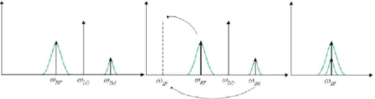
Figure 2.2 illustrates the image problem related to the Heterodyne Receiver.
Figure 2.2- Image problem in Heterodyne Receiver.
Considering that the input of the system is a RF modulated signal, it is possible to identify two bands: image is the band signal that is as distant to the LO frequency as the RF signal (the RF and IM signal are 2𝜔𝐼𝐹 apart from each other).
In fact, with an image rejection filter this signal is not completely clear and it will still be present, at the mixer input along with the signal of interest.
Considering only the mixing effect on the image signal, the output can be expressed by equation (2.1).
𝑦(𝑡) =𝑉𝐼𝑀.𝑉𝐿𝑂
2 cos((𝜔𝐼𝑚− 𝜔𝐿𝑂)𝑡) + 𝑉𝐼𝑀.𝑉𝐿𝑂
2 cos((𝜔𝐼𝑚+ 𝜔𝐿𝑂)𝑡) (2.1)
Considering the relation 𝜔𝐼𝑚= 2𝜔𝐿𝑂− 𝜔𝑅𝐹, the equation (2.1) can be re-written: 𝑦(𝑡) =𝑉𝐼𝑀.𝑉𝐿𝑂
2 cos((𝜔𝐿𝑂− 𝜔𝑅𝐹)𝑡) + 𝑉𝐼𝑀.𝑉𝐿𝑂
2 cos((3𝜔𝐿𝑂+ 𝜔𝑅𝐹)𝑡) (2.2)
One can see that one of the components coincides with the IF frequency, overlapping the desired signal, which implicates that the IF band must be thoroughly selected to prevent this constraint.
26
In retrospective, it can be said that the heterodyne receiver was developed to enable reception from numerous broadcasters.
Indeed, it works with several IF frequencies.
2.1.2 Homodyne Receiver
The Homodyne receiver depicted in Figure 2.3 [Ort, 2011] also known as Zero-IF receiver, directly translates to the baseband the input signal.
The aforementioned translation leads to a more elementary architecture and allows the possibility of complete integration given the fact that it does not imply high quality filters (such as the image rejection filter).
Figure 2.3- Quadrature Homodyne Receiver.
Nevertheless, because the signal is shifted to baseband, it is affected by flicker noise that is a low frequency noise, caused by active devices.
Moreover, it should be noted that this particular receiver does not guarantee perfect isolation between its blocks and as a consequence, oscillator leakage can occur.
The leakage is the result of ground problems and capacitive coupling, and can originate unwanted DC components, which eventually result in receiving process corruption.
2.1.3 Low IF Receivers
It was mentioned before that the homodyne receiver allows the possibility of full integration.
In terms of performance and flexibility, it is fair to say that the heterodyne receiver is better. Regardless this aspect, it requires external elements, so it does not allow complete integration.
In this sense, a new architecture, commonly known as Low IF receiver, arises from combining both receivers, ideally joining some important advantages of each receiver previously presented.
A mixed approach is used: basically the approach consists in using the homodyne receiver but instead of doing a direct conversion to baseband, the signal is shifted to allow intermediate frequency.
Thus, the baseband constraints are avoided. Regardless this consideration, it is still mandatory to overcome the image problem.
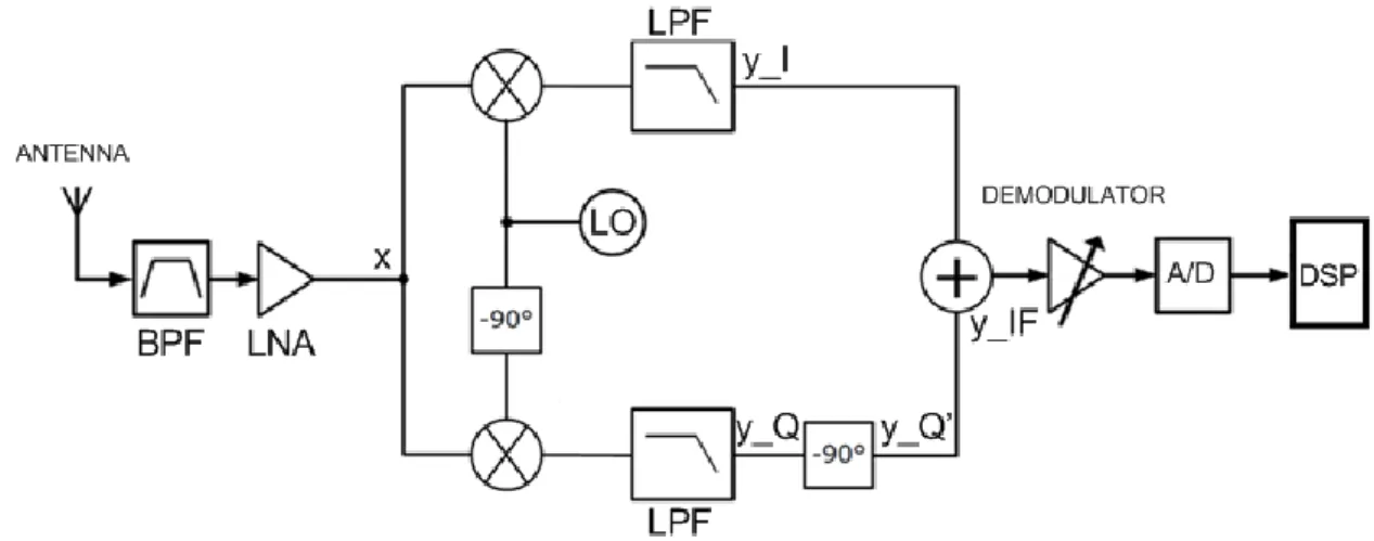
Since the main objective is to develop a receiver that allows fully integration instead of using a rejection filter to deal with the image signal, two extremely important image rejection techniques are used: the Hartley and Weaver architectures.
The idea is to process the signal after the low pass filter and combine both outputs into a single output.
This leads the image to be suppressed through its negative replica.
First, it will be explained and analyzed the Hartley architecture principle of functioning, detailed in Figure 2.4 [Ort, 2011].
28
Considering the following input .
𝑥(𝑡) = 𝑉𝑅𝐹cos(𝜔𝑅𝐹𝑡) + 𝑉𝐼𝑚cos(𝜔𝐼𝑚𝑡) (2.3) After low pass filtering
𝑦𝐼(𝑡) =𝑉𝑅𝐹2𝑉𝐿𝑂cos((𝜔𝐿𝑂− 𝜔𝑅𝐹)𝑡) +𝑉𝐼𝑚2𝑉𝐿𝑂cos((𝜔𝐼𝑚− 𝜔𝐿𝑂)𝑡) (2.4) 𝑦𝑄(𝑡) =𝑉𝑅𝐹2𝑉𝐿𝑂sin((𝜔𝐿𝑂− 𝜔𝑅𝐹)𝑡) +𝑉𝐼𝑚2𝑉𝐿𝑂sin((𝜔𝐼𝑚− 𝜔𝐿𝑂)𝑡)
Because a phase shift of -90 is realized on the quadrature signal 𝑦𝑄(𝑡)
𝑦𝑄(𝑡) =𝑉𝑅𝐹𝑉𝐿𝑂
2 cos((𝜔𝑅𝐹− 𝜔𝐿𝑂)𝑡) + 𝑉𝐼𝑚𝑉𝐿𝑂
2 cos((𝜔𝐿𝑂− 𝜔𝐼𝑚)𝑡) (2.5)
Finally, when the two signals, 𝑦𝐼𝐹(𝑡) and 𝑦𝑄(𝑡), are summed the image is suppressed
𝑦𝐼𝐹(𝑡) = 𝑉𝑅𝐹𝑉𝐿𝑂cos((𝜔𝑅𝐹− 𝜔𝐿𝑂)t) (2.6) The Weaver architecture is similar but is used a second mixer stage at the frequency𝜔𝐼𝐹.
Both solutions are dependent on the accuracy of the oscillators in terms of producing quadrature signals (phase and gain imbalances occur).
Regardless this fact, those deviations are far more noticeable in the Weaver approach because of the second mixer previously discussed since it introduces more phase deviations.
Figure 2.5 [Ort, 2011] presents a Low IF Receiver with Weaver Image Rejection.
2.2 CMOS Implementation Basic Concepts
2.2.1 Gain
In electronics the gain is one of the most important parameter of an amplifier. Specifically, the gain quantifies the ability of a given system to increase or decrease the amplitude of an input signal and it is determined as the ratio between the output and the input signal.
It is considered that a system has amplification when it presents a gain greater than one, and attenuation when it has a gain equal or less than one.
In the field of electronics two types of gain are normally considered (usually expressed in dB) and they are both expressed by equations (2.7) and (2.8).
𝑃𝑜𝑤𝑒𝑟 𝐺𝑎𝑖𝑛 = 10𝑙𝑜𝑔 (𝑃𝑜𝑢𝑡
𝑃𝑖𝑛) (2.7)
𝑉𝑜𝑙𝑡𝑎𝑔𝑒 𝐺𝑎𝑖𝑛 = 20𝑙𝑜𝑔 (𝑉𝑜𝑢𝑡
𝑉𝑖𝑛) (2.8)
The base element of a CMOS circuit is the MOSFET transistor.
It can assume different behaviors according to its operation region as shown in Figure 2.6, which is defined by the biasing voltages.
Considering the saturation region the drain current produced by the transistor is approximated given by Equation (2.9):
𝐼𝐷= 𝑘𝑝/𝑛1 2
𝑊
𝐿(𝑉𝑔𝑠− 𝑉𝑡ℎ
2) (2.9)
where k is the mobility constant and it is a technology parameter (𝑘𝑝 refers to PMOS transistors and 𝑘𝑛 refers to NMOS transistors), 𝑊 is the width of the transistor, 𝐿 is the length of the transistor, 𝑉𝑔𝑠 is the gate-to-source voltage drop and 𝑉𝑡ℎ is the threshold voltage (transistor operating voltage).
In this region the drain current is weakly dependent upon drain voltage and it is controlled essentially by the gate-source voltage (considering small variations of the threshold voltage).
Figure 2.6 presents MOSFET N-Type model and Figure 2.7 illustrates MOSFET regions [Lop, 2010]
30 Figure 2.6- MOSFET N-type Model.
Figure 2.7- MOSFET regions.
Considering the facts aforementioned, it is possible to obtain the I-V characteristic of the transistor and define the MOSFET transconductance, given by Equation (2.10) which is a current gain and a key design parameter for a transistor [Lee, 2004].
Figure 2.8- I-V curve and transconductance.
𝑔𝑚=𝛿𝑉𝛿𝐼𝐷
𝑔𝑠 (2.10)
It is also possible to calculate the general voltage gain if a load with resistance 𝑅𝑜𝑢𝑡 is applied, expressed by Equation (2.11).
𝐴 = 20𝑙𝑜𝑔(𝑔𝑚𝑅𝑜𝑢𝑡) (2.11)
To prevent parasitic coupling, the bulk must be at the same voltage potential as the source in a NMOS transistor and the same voltage potential as the drain in a PMOS transistor.
Nevertheless, this is not always guaranteed. Considering the NMOS case (the development of the circuit related to this thesis, only required the use of NMOS transistors) the body effect describes how much the threshold voltage is affected by the change in the source-bulk voltage. This effect, expressed in a constant 𝛾, is expected in differential pairs and diode connected NMOS [Lee, 2004].
32 Figure 2.9- Body effect demonstrated using small signal analysis.
The Equation 2.12 relates the body effect and threshold voltage:
Δ𝑉𝑡ℎ= 𝛾 (√2|𝜙𝑝| + 𝑉𝑠𝑏− √2|𝜙𝑝|) (2.12)
𝜙𝑝 is the surface potential parameter and 𝑉𝑠𝑏 is the source to bulk voltage.
This effect leads to the appearance of an extra transconductance term (Equation 2.13). 𝑔𝑚𝑏= −𝑖𝑑𝑠 𝑉𝑠𝑏= − 𝜕𝐼𝑑𝑠 𝜕𝑉𝑠𝑏= − 𝜕𝐼𝑑𝑠 𝜕𝑉𝑡ℎ 𝜕𝑉𝑡ℎ 𝜕𝑉𝑠𝑏, with constant 𝑉𝑑𝑠, 𝑉𝑔𝑠 (2.13) 𝑔𝑚𝑏= 𝛾 2√2|𝜙𝑝|+𝑉𝑠𝑏 𝑔𝑚=𝐶𝐶𝑠 𝑜𝑥𝑔𝑚= 𝜂𝑔𝑚, with 0.1 ≤ 𝜂 ≤ 0.3
The aforementioned “extra” transconductance is related to the current consumption and is equivalent from 10 % up to 30 % of the 𝑔𝑚 value.
Given the fact that the transconductance parameter is vital in CMOS design this effect must be taken into consideration for the best approaches, hence, for the best results.
Some considerations present not only in chapter three, but also in chapter four, will highlight the importance of this parameter.
2.2.2 Input Impedance
When conceiving complex structures as a RF receiver, some blocks are cascaded together.
Regardless, the connection between the blocks can be realized immediately. Typically, the output impedance of one block is different to the input impedance of the following one, which reflects back in the amount of power transferred between the devices [Ort, 2011].
In this sense, it is crucial not only to identify the input impedance of one device, but also how it can be adapted to maximize power transfer.
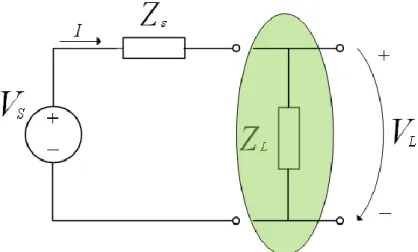
The input impedance is the one seen by the power source. It can be modeled by a Thevenin Equivalent.
Figure 2.10 presents an equivalent system input assuming reactive load.
Figure 2.10- Equivalent system input assuming reactive load.
Briefly, 𝑉𝑆 is the voltage supply source, 𝑍𝑆 is the source impedance and 𝑍𝐿 is the impedance of the load network.
Considering the classical Ohm’s law, the current that flows through the circuit can be expressed by Equation 2.14.
|𝐼| = |𝑉𝑆|
|𝑍𝑆+𝑍𝐿|=
|𝑉𝐿|
|𝑍𝐿| (2.14)
To obtain the condition that guarantees the maximization of power transfer it is mandatory to determine the power delivered to the load:
34 𝑃 = 𝐼𝑅𝐿 =1 2|𝐼| 2𝑅 𝐿=12(|𝑍|𝑉𝑆+𝑍𝑆|𝐿|) 2 𝑅𝐿 (2.15) =1 2 |𝑉𝑆|2𝑅𝐿 (𝑅𝑆+ 𝑅𝐿)2+ (𝑋𝑆+ 𝑋𝐿)2
Synthetically, resistance 𝑅𝑆 and reactance 𝑋𝑆 are the real and imaginary parts of 𝑍𝑆 and the same considerations can be applied for the resistance 𝑅𝐿 and reactance 𝑋𝐿 but related to 𝑍𝐿. The condition that maximizes the power transfer can be calculated by differentiating the above equation with respect to 𝑍𝐿 and equalize to zero:
𝛿𝑃
𝛿𝑍𝐿= 0 <=> 𝑍𝑆= −𝑍𝐿 (2.16)
According to Equation 2.16, load and source impedances should be complex conjugates of each other to guarantee the maximization of power transfer between the two systems.
Likewise, this is also relevant for the inter-connections receiver’s RF blocks. Not only input but also output impedance of each single block must be characterized for appropriate connection.
Often an impedance match must be realized to adapt the impedances.
Merely as an example, this is critical at the input of the LNA, since as previously studied on other subjects, the antenna has a characteristic impedance of 50 ohms and it captures a weak signal, the receiver must not lose power.
Because of this, the LNA has to be designed very thoroughly in order to match the antenna impedance.
Given the circumstances of dealing with CMOS technology, blocks present in its constitution, MOSFET transistors, which have typically a resistive or capacitive input.
It is also crucial to mention that capacitive match must be realized through the use of inductors which results sometimes in constraints in CMOS design mainly because of area consumption.
2.2.3 Quality Factor
The Quality Factor (𝑄) is the most common figure of merit for oscillators, and it is associated to the local oscillator phase-noise. 𝑄 is usually defined within the context of second order systems.
In fact, this particular figure of merit is extremely important to the realization of the proposed approach, because one of the fundamental goals of the present work, is to force the circuit to oscillate. And to realize this task, it is important to investigate the value of 𝑄-factors (in this case, ideally, higher 𝑄- factors).
Synthetically, there are three definitions of 𝑄 that gather consensus in the scientific community:
(1) The first definition is assumed considering a bandwidth calculated for -3 dB and a carrier frequency 𝜔0:
𝑄 =𝜔0
𝐵 (2.17)
This is applied to filters and oscillators characterized as second order resonant circuits.
Below is shown Figure 2.11 [Oli, 2008] that summarize Q-factor for a second order system.
Figure 2.11- Q definition for a second order system.
Due to considerations previously studied it is known that the transfer function of a second order bandpass filter can be expressed as:
𝐻(𝑠) = 𝐾𝜔0𝑄𝑠
36
K is the mid-band gain and 𝑄 is the pole quality factor. For 𝑄 ≫ 1 the transfer function is symmetric as shown in figure 2.11.
This definition of 𝑄 is reasonable for filters and can be used for oscillators. However it is important to consider the resonator circuit as a second order filter. (2) A second definition of 𝑄, can be expressed through Equation 2.19, considers
a given circuit and associates the maximum energy stored and the energy dissipated in a period.
(3)
𝑄 = 2𝜋𝑀𝑎𝑥𝑖𝑚𝑢𝑚 𝑒𝑛𝑒𝑟𝑔𝑦 𝑠𝑡𝑜𝑟𝑒𝑑 𝑖𝑛 𝑎 𝑝𝑒𝑟𝑖𝑜𝑑𝐸𝑛𝑒𝑟𝑔𝑦 𝑑𝑖𝑠𝑠𝑖𝑝𝑎𝑡𝑒𝑑 𝑖𝑛 𝑎 𝑝𝑒𝑟𝑖𝑜𝑑 (2.19)
The Equation (2.19) is normally related to a common RLC circuit and associates the maximum energy stored (in C or L) and the energy dissipated (by R) in a period.
As a mere example, this second definition can be applied to an RLC series circuit. The energy is stored in the inductor and in the capacitor, and the maximum energy stored in the inductor and the capacity is equal.
Correspondingly, the energy stored in an inductor (𝑊𝐿) can be expressed as: 𝑊𝐿= ∫ 𝑖(𝑡)0𝑇 𝐿𝑑𝑖(𝑡)𝑑𝑡 𝑑𝑡 = 𝐿𝐼𝑟𝑚𝑠2 (2.20) 𝐼𝑟𝑚𝑠 is the root-mean-square current in the inductor.
The energy dissipated in a resistor (𝑊𝑅) per cycle (in the period 𝑇0) is: 𝑊𝑅= 𝐼𝑟𝑚𝑠2 𝑅𝑇
0 (2.21)
Then, the value of 𝑄-factor is:
𝑄 = 2𝜋 𝐿𝐼𝑟𝑚𝑠2 𝐼𝑟𝑚𝑠2 𝑅𝑇0= 2𝜋𝑓0 𝐿 𝑅= 𝜔0𝐿 𝑅 (2.22)
Likewise, it is also plausible to express the energy stored in the capacitor: 𝑊𝑐 = ∫ 𝑣(𝑡)0𝑇 𝐶𝑑𝑣(𝑡)
𝑑𝑡 𝑑𝑡 = 𝐶𝑉𝑟𝑚𝑠
In the Equation 2.23, 𝑉𝑟𝑚𝑠2 is the root-mean-square voltage in the capacitor, and 𝑉𝑟𝑚𝑠 =(𝜔𝐼𝑟𝑚𝑠
0𝐶)
In this sense, the value of 𝑄 is:
𝑄 = 2𝜋 𝐶𝑉𝑟𝑚𝑠2 𝐼𝑟𝑚𝑠2 𝑅𝑇0= 2𝜋𝑓0 𝐶𝐼𝑟𝑚𝑠2 𝜔02𝐶2 𝑅𝐼𝑟𝑚𝑠2 = 1 𝜔0𝐶𝑅 (2.24)
(4) In the third and final definition of 𝑄 the oscillator is taken as a feedback system and the phase of the open-loop transfer function 𝐻(𝑗𝜔) is evaluated at the oscillation frequency, 𝜔𝑜𝑠𝑐 and is not necessarily the resonance.
In a single RLC circuit the oscillation frequency is the resonance frequency, but with coupled oscillators the oscillation frequency may be distinct.
To clarify the third definition, the oscillator 𝑄 can be defined as: 𝑄 =𝜔0 2 √ ( 𝑑𝐴 𝑑𝜔) 2 + (𝑑𝜃 𝑑𝜔) 2 (2.25)
Additionally, A is the amplitude and 𝜃 is the phase of 𝐻(𝑗𝜔). This definition, called open loop 𝑄 considers the amplitude and phase fluctuations of the open-loop transfer function.
This 𝑄 definition is frequently related to a single resonator, and to demonstrate that Figure 2.12 is presented [Oli, 2008].
Figure 2.12- Definition of Q based on open-loop phase slope.
In fact, the last definition is an important “tool” to obtain the oscillator quality factor, which has its higher value at the resonance frequency.
38
2.3 Oscillators
Synthetically, it can be said that an oscillator converts a given DC level in pure sine-wave signal. It is of significant importance in terms of blocks in a receiver, because the quality of a down-conversion depends on the quality of the oscillator signals.
In terms of groups, it is possible to divide oscillators into two major groups: quasi-linear and strongly non-quasi-linear oscillators.
The second group, referred to strongly non-linear or relaxation oscillators, are typically performed by RC-active circuits.
The primary advantage of this group of oscillators lies in the fact that only resistors and capacitors are used together with the active devices.
In terms of disadvantages that relaxation oscillators present, the most obvious one, is their phase-noise value, which is high.
LC oscillators are normally quasi-linear oscillators. As resonator element, LC oscillators can use dielectric resonators, crystals, striplines, and LC tanks.
These oscillators are known by their good phase-noise performance, since 𝑄 is normally much higher than unity.
LC Oscillators
The LC oscillator, as shown in Figure 2.13, is a pure reactance feedback circuit. Synthetically, the circuit presents a differential pair operating as a commutator. The aforementioned differential pair will be responsible to alternate the current conduction path through the feedback network thus producing an alternate signal.
Figure 2.13- LC Oscillator.
Considering the fact that in a practical context the feedback network evidently present losses, the differential pair presents cross coupled outputs for compensation (thereby respecting the conditions relative to the Barkhausen criterion).
It is known that the small signal equivalent of the mentioned differential pair “imitates” a negative resistance. Indeed, the circuit can be modeled as Figure 2.14 shows.
40
Regardless the advantage of normally presenting a high quality factor value (current is exchanged between the capacitor and inductor), a low phase noise and a quasi-linear behavior, LC oscillators also present some disadvantages.
For instance, considering the fact that the feedback network parameters are fixed (𝜔0= 1
√𝐿𝐶), these oscillators have low frequency tuning capability.
Additionally, the integration in CMOS technology would definitely require large area consumption and this situation requires additional costs.
To conclude the considerations related to the LC oscillators drawbacks, it is fair to mention that modern receivers require quadrature outputs.
This type of oscillator, by itself, is not able to provide.
As a way to overcome the aforementioned constraint, it is possible to coupling an additional oscillator, but it will increase even more the area consumption and will contribute to the degradation of the frequency response because of the additional parasitic capacitances.
RC Oscillators
Literature shows that there has been a great interest in the last decade over the study and design of this type of oscillators.
If we establish a comparison in terms of area consumption between LC oscillators and RC oscillators, the second ones occupy far less area and they present other advantage: RC oscillators are highly integrable.
Regarding to structure and behavior, a RC oscillator is very similar to the one encountered in the LC oscillator.
In terms of quality factor, it is important to emphasize a difference in regard of the assumptions previously discussed about LC oscillators.
In RC Oscillators the feedback network is constituted by a capacitor and a resistor, which results in a lower 𝑄 factor.
This type of oscillator has the same differential pair that is responsible for the loss compensation and commutation behavior.
The capacitor is responsible to transform the DC current into voltage (Equation 2.26) and the resistor is used for biasing.
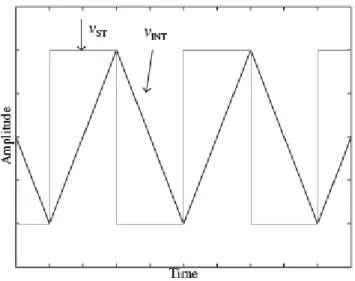
The Figure 2.15 shows a common RC oscillator, more precisely the relaxation Oscillator.
𝑣(𝑡) =1
𝐶∫ 𝑖(𝜏) 𝑡
Figure 2.15- Relaxation oscillator.
It is known that the block diagram of a relaxation oscillator, can be modelled using an integrator and a Schmitt trigger [Oli, 2008].
The Schmitt- trigger is a memory element, and controls the sign of the integration constant.
Below, the oscillator waveforms are presented in Figure 2.16. It is important to mention that the square waveform is the Schmitt-trigger output, and the triangular waveform is the integrator output.
42
To implement the oscillator at very high frequencies we need a circuit as simple as possible (Figure 2.15).
In this sense, we should replace the integrator and the Schmitt trigger by simple circuits that ensure some correspondence between the high level and the circuit level.
The integrator previously discussed is implemented simply by a capacitor (Figure 2.17).
Figure 2.17- a) Integrator implementation. b) Integrator waveforms.
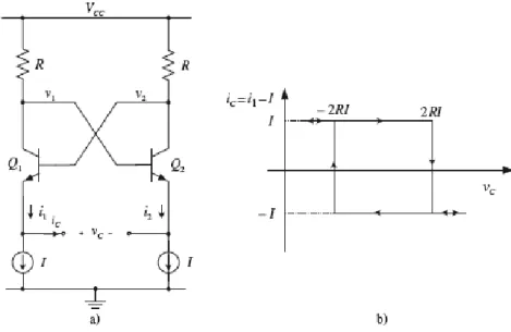
Its input is the capacitor current (𝑖𝐶) and the output is the capacitor voltage (𝑣𝐶). This voltage is the input of the Schmitt-trigger (Figure 2.18), the output of which is 𝑖𝐶. The transfer characteristic of the aforementioned Schmitt-trigger is shown in Figure 2.18b.
It is important to mention that it is assumed that the switching occurs abruptly when the sign of 𝑣𝐵𝐸1− 𝑣𝐵𝐸2 changes.
Figure 2.18- Schmitt- trigger: a) Circuit implementation. b) Transfer characteristics.
Regardless the fact that in terms of the model related to the Figure 2.16 the Schmitt-trigger output is 𝑖𝐶, it is important to use as the oscillator output the voltage 𝑣𝑂𝑈𝑇 = 𝑣1− 𝑣2, with an amplitude of 4IR, as shown in Figure 2.19.
Figure 2.19- Relaxation oscillator waveforms.
At very high frequencies the outputs are approximately sinusoidal with an amplitude lower than 4IR. A circuit with MOS transistors has the exact performance as described above.
The circuit presented in Figure 2.15 is one possible implementation, the oscillator integration constant is I/C and the amplitude is 4IR.
The resonant frequency is expressed through Equation 2.27.
𝑓 = 1
2𝐶(4𝑅𝐼)= 1
8𝑅𝐶 (2.27)
Designing this type of oscillator in CMOS technology, provides an interesting advantage, since the capacitor can be materialized by the simple presence of the MOS parasitic capacitances, which will reduce the area needed for implementation [Wes, 1998].
Next in subchapter 2.3.1 and 2.3.2, it will be addressed not only a well-known criterion, as well as an important measure of performance of an oscillator.
2.3.1 Barkhausen Criterion
The basic objective of an oscillator is to convert a DC signal into a periodic signal. A sinusoidal oscillator generates a sinusoid with frequency 𝜔0 and amplitude 𝑉0.
44
𝑣𝑂𝑈𝑇(𝑡) = 𝑉0cos(𝜔0𝑡 + 𝜃) (2.28)
For digital purposes, oscillators generate a clock signal (square-waveform with period 𝑇0).
Figure 2.20 [Oli, 2008] shows a sinusoidal oscillator output in time domain and Figure 2.21 shows the aforementioned output in frequency domain [Oli, 2008].
As shown in Figure 2.22, sinusoidal oscillators can be interpreted as a feedback system, with the transfer function expressed by the Equation (2.29).
𝑌𝑜𝑢𝑡(𝑗𝜔)
𝑋𝑖𝑛(𝑗𝜔) =
𝐻(𝑗𝜔)
1−𝐻(𝑗𝜔)𝛽(𝑗𝜔) (2.29)
Figure 2.20- Sinusoidal oscillator output in time domain.
Figure 2.21- Sinusoidal oscillator output in frequency domain.
The necessary conditions related to the loop gain for steady-state oscillation with frequency 𝜔0 are known as the Barkhausen conditions.
Figure 2.22 presents a feedback system block diagram [Oli, 2008].
Figure 2.22- Feedback system block diagram.
Below it will be addressed the aforementioned conditions.
The loop gain has to be unity (this is the gain condition), and the open-loop phase shift must be 2𝑘𝜋, where 𝑘 is obviously an integer including zero (this is the phase condition).
|𝐻(𝑗𝜔0)𝛽(𝑗𝜔0)| = 1 (2.30)
𝑎𝑟𝑔[𝐻(𝑗𝜔0)𝛽(𝑗𝜔0)] = 2𝑘𝜋 (2.31)
The Barkhausen criterion is very important because it gives the appropriate and necessary conditions for stable oscillations. Nevertheless, does not guarantee the start of oscillation.
This means that for a circuit to oscillate, or in other words, for the oscillation to start, triggered by noise, when the system is switched on, the loop gain must be greater than unity, |𝐻(𝑗𝜔0)𝛽(𝑗𝜔0)| > 1 [Lee, 2001].
2.3.2 Phase-noise
In modern transceiver applications, the most significant difference between ideal and real oscillators is the phase-noise [Raz, 1996].
The noise generated at the oscillator output originates random fluctuation of the output amplitude and phase.
This implies that the output spectrum has bands around 𝜔0 and its harmonics. The noise can be generated inside the circuit, or outside the circuit: inside due to passive and active devices and outside due to power supply.
Some effects, such as nonlinearity and periodic variation of circuit parameters make it very difficult to foresee phase-noise.
46
The noise causes fluctuations of both amplitude and phase.
The oscillator noise can be characterized in two domains: the frequency domain (phase-noise), or in the time domain (jitter).
The first one is used by analog and RF designers, while the second is used by digital designers.
There are numerous ways to quantify the variations of phase and amplitude in oscillators.
Normally, they are characterized in terms of the single sideband noise spectral density, ℒ(𝜔), expressed in decibels below the carrier per hertz (dBc/Hz).
This characterization makes sense for all types of oscillators and can be described as:
ℒ(𝜔𝑚)=𝑃(𝜔𝑚)
𝑃(𝜔0) (2.32)
In Equation 2.32 𝑃(𝜔𝑚) is the single sideband noise power at a distance of 𝜔𝑚 from the carrier 𝜔0 in a 1 Hz bandwidth and 𝑃(𝜔0) is the carrier power.
The advantage associated with this parameter is related to its ease in terms of measurement.
This can be done in two ways: 1) with the use of a spectrum analyzer, which is a general-purpose equipment, but will definitely provide errors; 2) with phase or frequency demodulators with particular and well known properties.
In regard to Equation 2.32, the spectral density includes not only phase noise, but also amplitude noise, and it should be noted that they cannot be separated.
Regardless this fact, practical oscillators have an amplitude stabilization mechanism, which strongly reduces the amplitude noise, while the phase-noise is unaffected.
The Equation 2.32 is dominated by the phase-noise, so ℒ(𝜔𝑚) is known merely as phase-noise.
The carrier-to-noise ratio (CNR) can also be used to describe the oscillator phase-noise.
Figure 2.23 shows the spectrum of oscillator output with phase noise [Oli, 2008]. The CNR in a 1 Hz frequency band at the distance of 𝜔𝑚 from the carrier𝜔0, can be described through the Equation (2.33).
𝐶𝑁𝑅(𝜔𝑚) =ℒ 1
Figure 2.23- Spectrum of oscillator output with phase.noise.
2.3.3 Importance of Phase Noise in Wireless Communications
The phase-noise in the local oscillator will spread the power spectrum around the oscillation frequency of interest.
As a consequence of this fact, the immunity against adjacent interferer signals will be restricted.
Notably, in the receiver path it is intended to down convert a specific channel located at a given distance from the oscillator frequency; due to the oscillator phase-noise, not only the desired channel is downconverted to an intermediate frequency, but also the nearby channels or interferers, corrupting the wanted signal.
This phenomenon is usually called “reciprocal mixing”.
In the case of the transmitter path the phase-noise tail of a strong transmitter can corrupt and overwhelm close weak channels.
As a mere example, if a receiver detects a weak signal at 𝜔2, this will be affected by a close transmitter signal at 𝜔1 with significant phase-noise.
Figure 2.24 shows the phase-noise effect on the receiver and the unwanted down conversion [Oli, 2008] and Figure 2.25 presents the phase-noise phenomenon on the transmitter path [Oli, 2008].
48 Figure 2.24- Phase-noise effect on the receiver and the unwanted down
conversion.
Chapter 3.
CMOS Active Inductors
3.1 Definition and characteristics
CMOS Active inductors (AI) are active networks that consist essentially of MOS transistors.
Resistors are often used as feedback elements to optimize the performance of active inductors.
Through certain dc biasing conditions and signal-swing constraints, AI exhibit an inductive characteristic in a specific frequency range.
In this sense, it is crucial to highlight some attractive advantages that CMOS active inductors offer.
Low silicon area: Given the fact that just MOS transistors are normally required
in the realization of CMOS active inductors and the inductance of the aforementioned networks, is inversely proportional to the transconductances of the MOS transistors, the silicon consumption of CMOS active inductors is insignificant.
Large and tunable inductance: The smaller the width of the transistors, the larger
the inductance.
Besides this fact, the inductance can be tuned appropriately by differing the dc biasing condition of the transistors synthesizing the inductor with a large inductance tuning range.
Large and tunable self-resonant frequency: The passband center frequency of
an active inductor RF bandpass filter is normally set to the self-resonant frequency of the AI of the filter.
In chapter four, it will be clear that the larger the self-resonant frequency of the AI, the higher the passband center frequency of the filter.
To conclude these considerations, it can be said that a large self-resonant frequency of active inductors ensures that the active inductors will have an inductive characteristic over a large frequency range.
Large and tunable quality factor: The quality factor of CMOS active inductors is
defined with the ohmic loss of the inductors, arising essentially from the finite output resistance of the transconductors of the inductors.
In fact, the quality factor of CMOS AI can be maximized through the increase of the output resistance [Oli, 2011].
50
There are several strategies to increase the output resistance. Just as an example, it can be referred cascodes, regulated cascodes or negative resistor compensation. However it is important to highlight the fact that each one of these methods has its own degree of compensation, that is, every single one can be varied.
Considering the first method discussed, the cascode approach, the output resistance of a cascade-configured transconductor can be adjusted by changing the biasing voltage of the cascading transistor.
Compatibility with digital CMOS technologies: CMOS active inductors can be
performed with the use of standard digital CMOS processes.
Regardless some attractive advantages that CMOS active inductors offer, they present several disadvantages.
As an example, although they reveal an extraordinary ability to optimize the control of the quality factor, typically Active Inductors have a low quality factor.
In summary, one can say that higher noise, nonlinearity and power consumption are the major disadvantages of active inductors due to the fact that these circuits are realized using active devices which have higher noise.
Several of the active inductors configurations considered in previous work can be simplified to the model shown in Figure 3.1.
It is important to mention that the aforementioned figure presents Newton’s notation for differentiation, also known as the dot notation for differentiation.
Figure 3.1 – Simplified model of AI configuration.
Figure 3.2 represents the phasor diagram that describes the operation of the model previously discussed.
Figure 3.2 – Phasor diagram that illustrates the operation of the simplified model.
In fact, considering a sinusoidal input voltage 𝑉̇𝑖𝑛 applied to the active two-port situated within the dotted line of Figure 3.1, the controlled current source 𝑔𝑚1𝑉̇𝑖𝑛.realizes the current expressed in Equation 3.1:
𝐼̇𝐶= 𝑔𝑚1𝑉̇𝑖𝑛 (3.1)
Assuming that the voltage 𝑉̇𝐶= −𝑗 [(𝑔𝑚1
𝜔𝐶)] 𝑉̇𝑖𝑛 at the capacitor C is responsible or used for control another current source, in circumstance 𝑔𝑚2𝑉̇𝐶, which develops the current:
𝐼̇𝐿= 𝑔𝑚2𝑉̇𝐶 = −𝑗 [(𝑔𝑚1𝑔𝑚2
𝜔𝐶 )] 𝑉̇𝑖𝑛 (3.2)
The input current can be expressed as follows:
𝐼̇𝑖𝑛= 𝐼̇𝐶+ 𝐼̇𝐿= 𝑉̇𝑖𝑛𝑌̇𝑖𝑛 (3.3)
The input impedance 𝑌̇𝑖𝑛 is equal to 𝑔𝑚1− 𝑗 [(𝑔𝑚1𝑔𝑚2
𝜔𝐶 )] (3.4)
This means that 𝑌̇𝑖𝑛 possesses the necessary inductive component. The Figure 3.3 (3.3) is related to the equivalent circuit of the two-port that will include the inductance
𝐿𝑜𝑒 =(𝑔 𝐶
𝑚1𝑔𝑚2) (3.5)
Shunted by the resistor 𝑅𝑜𝑒=𝑔1
52 Figure 3.3 – Equivalent circuit of the two-port.
Normally, designers try to minimize the influence of the resistance aforementioned. This objective centered in the reduction of the influence indicated, can be reached by two methods:
1) By selecting accurately the parameters 𝑔𝑚1 and 𝑔𝑚2.
2) Choosing accurately the parameters of the specific circuit where the active inductor is employed.
3.2 Proposed approach
Equation 3.3 shows that the input current 𝐼̇𝑖𝑛, has in its constitution the component 𝐼̇𝐶. This is actually an active component for the input current and the strategy embraced relates to a compensation of this particular component. The compensation process results by adding a third current source −𝑔𝑚1𝑉̇𝑖𝑛 = −𝐼̇𝐶.
In terms of the components that the input current now includes, with this compensating current, it is only noted the inductive component 𝐼̇𝐿.
In other words, it can be said that the compensated two-port behaves as a pure inductor.
Although this compensation may seem complicated, since the third current source involves the addition of an inverting transconductance amplifier, previous work proved that this is possible just by associate one additional transistor.
It is important to say that this approach changes the point of view on design of active inductors shown in Figure 3.1.
Indeed, this modified design provides an interesting control in regard of Q-factor, that is, it is possible to achieve high Q-factor stable active resonators.
Figure 3.4 shows the two-port with inductive input current and Figure 3.5 demonstrates the compensation process and how the current seen by the input voltage source becomes purely inductive.
Figure 3.4 – Two- port with inductive input current.
Figure 3.5 – Compensation of the component 𝐼̇𝐶.
The modification previously discussed is shown in Figure 3.4, and it is fair to mention that it modifies the properties of basic configuration.
Additionally, will be presented next Figure 3.6, which embodies the realizations of the basic model and, evidently, the model with compensation of the active component in the input current.
M1 IB2 IB1 M2 vin M3 -1 Cgs2 M1 IB2 IB1 M2 Cgs2 vin a) b) VDD VDD
Figure 3.6 – a) Standard realization and b) the addition of the compensation source.
54
It is crucial to note that the circuits use the capacitor 𝐶𝑔𝑠2 to make the compensation process a reality. Taking into consideration this compensation, through the use of small-signal models and by analyzing Figure 3.7 it is possible to establish a comparison between the two circuits.
b) a)
v
gs2g
m1v
inC
gs1v
ini
ing
m1v
inC
gs2g
m2v
gs2 _C
gs1v
ini
inv
gs2g
m3v
in _g
m2v
gs2 _C
gs2Figure 3.7 – Small signal analysis of circuits of figure 3.6.
Considering Figure 3.7 the Equation (3.6) and Equation (3.7) can be written:
𝑖𝑖𝑛= 𝑔𝑚1𝑣𝑖𝑛− (−𝑔𝑚2𝑣𝑔𝑠2) + 𝑠𝐶𝑔𝑠1𝑣𝑖𝑛 (3.6)
and 𝑣𝑔𝑠2= ( 1
𝐶𝑔𝑠2) (𝑔𝑚1𝑣𝑖𝑛) (3.7)
Substituting (3.7) into (3.6), the input admittance of the circuit given in figure 3.7, can be expressed as follows:
𝑌𝑖𝑛 = 𝑔𝑚1+𝑔𝑚1𝑔𝑚2 𝑠𝐶𝑔𝑠2 + 𝑠𝐶𝑔𝑠1= 1 𝑅𝑜𝑒+ 1 𝐿𝑜𝑒+ 𝑠𝐶𝑜𝑒 (3.8) 𝑅𝑜𝑒 =𝑔1 𝑚1, 𝐿𝑜𝑒= 𝐶𝑔𝑠2 (𝑔𝑚1𝑔𝑚2) and 𝐶𝑜𝑒= 𝐶𝑔𝑠1
In fact, this active inductor can be associated to a parallel RLC circuit, since in a practical perspective, it resumes in an active resonator. In chapter four, it will be presented the theoretical and simulation results of the parallel RLC-circuit.
The resonance frequency of the circuit is given by:
𝜔𝑝= 1
√𝐿𝑜𝑒𝐶𝑜𝑒= √(𝑔𝑚1𝑔𝑚2)/(𝐶𝑔𝑠1𝐶𝑔𝑠2) (3.9)
𝑄 = 𝜔𝑝𝐶𝑜𝑒𝑅𝑜𝑒= √(𝑔𝑚2/𝑔𝑚1√𝐶𝑔𝑠1/𝐶𝑔𝑠2 (3.10)
Regardless the constitution of Equation 3.10, in terms of sizing (this consideration will be more detailed in chapter four) it was decided to choose the same value of transconductance for 𝑔𝑚1 and 𝑔𝑚2, and capacitors 𝐶𝑔𝑠1
Normally, designers are interested to control resonance frequency and Q-factor, independently. Through previous work, it is known that by analyzing the circuit shown in figure 3.7, input admittance is:
𝑌𝑖𝑛 = 𝑔𝑚1− 𝑔𝑚3+ (𝑔𝑚1𝑔𝑚2)/(𝑠𝐶𝑔𝑠2) + 𝑠𝐶𝑔𝑠1 (3.11) In terms of 𝑄-factor, there is a difference in terms of the value of 𝑅𝑜𝑒, that is: 𝑅𝑜𝑒=(𝑔 1
𝑚1−𝑔𝑚3). This means that Q-factor equation becomes:
𝑄 = ( 1 𝑔𝑚1−𝑔𝑚3) √
𝐶𝑔𝑠1
𝐶𝑔𝑠2√𝑔𝑚1𝑔𝑚2 (3.12)
Equations (3.11) and (3.12) emphasizes the idea that the addition of a compensating circuit, provides the advantage of better control of the Q-factor of the equivalent RLC-circuit.
Indeed, this control is extremely important whenever active inductors are involved and the chapter dedicated to the simulation process highlight the key role that this control took during the realization of the present work.
It should be mentioned the fact that to improve the drive of 𝐼𝐷1 (drain current of 𝑀1) into the gate-to-source capacitor of 𝑀2, it is used cascoding at the drain of 𝑀1.
In this sense, Figure 3.8 presents the cascoding at the drain of 𝑀1.
Moreover, it is important to highlight the fact that each one of the current sources presented in the proposed circuit is ideal.
56 M6 M2 VDD M1 IB2 IB1 Vin Cblocking
Figure 3.8 – Cascoding at the drain 𝑀1.
Indeed, this control is extremely important whenever active inductors are involved and the chapter dedicated to the simulation process highlight the key role that this control took during the realization of the present work.
The cascoding above discussed is responsible for the compensation of active component in the circuit.
The drive from the input to the source of cascoding transistor gives the necessary gain of −𝑔𝑔𝑚1
𝑚6 in regard to the input signal. The addition of one transistor, in this case 𝑀3,
guarantees the desired compensation.
Figure 3.9 shows the introduction of the aforementioned device in order to achieve the compensation discussed.
M6 M2 VDD M1 IB2 IB1 Vin Cblocking M3
Figure 3.9 – Addition of transistor 𝑀3 to the realization of the required
compensation.
The input admittance associated to figure 3.9 can be described as:
𝑌𝑖𝑛 = 𝑔𝑚1−(𝑔𝑚3𝑔𝑚1)
𝑔𝑚6 + (
(𝑔𝑚1𝑔𝑚2)
𝑠𝐶𝑔𝑠2 ) + 𝑠𝐶𝑔𝑠1 (3.13)
In terms of resonance frequency, there is no variation. But the quality factor of this active inductor is given by:
𝑄 = ((𝑔1 𝑚1) − ( 𝑔𝑚1𝑔𝑚3 𝑔𝑚6 )) √ 𝐶𝑔𝑠1 𝐶𝑔𝑠2√𝑔𝑚1𝑔𝑚2 (3.14)
Chapter 4.
Prototype Design and Simulation Results
4.1 Initial premises of first sizing
The design process and all simulations carried out in the present chapter, refer to the circuit show in Figure 3.8.
To clarify this fact, the aforementioned figure is purposely presented again.
M6 M2 VDD M1 IB2 IB1 Vin Cblocking
Figure 4.1 – The proposed circuit.
In order to study and comprehend all the relevant premises related to the circuit with the maximum possible property, firstly it was decided to proceed to the design of transistors 𝑀1 and 𝑀2 and setting 𝑊6 and 𝐿6, of transistor 𝑀6.


![Figure 2.5 [Ort, 2011] presents a Low IF Receiver with Weaver Image Rejection.](https://thumb-eu.123doks.com/thumbv2/123dok_br/15470570.1034128/29.892.128.766.853.1084/figure-ort-presents-low-receiver-weaver-image-rejection.webp)