Fábio Moreira de Passos
Licenciado em Engenheiria Electrotécnica e de Computadores
Modeling of Integrated Inductors for RF
Circuit Design
Dissertação para obtenção do Grau de Mestre em Engenharia Electrotécnica
Orientadora :
Maria Helena Fino, Assistant Professor,
FCT-UNL
Co-orientadora :
Elisenda Roca Moreno, Tenured Scientist,
Uni-versity of Seville and IMSE-CSIC
Júri:
Presidente: Fernando Coito
Arguente: João Pedro Oliveira
iii
Modeling of Integrated Inductors for RF Circuit Design
Copyright cFábio Moreira de Passos, Faculdade de Ciências e Tecnologia, Universidade Nova de Lisboa
Acknowledgements
First of all I would like to address a true appreciation to the Department of Electrical Engineering of the Faculty of Science and Technology as a learning institution and to Seville Institute of Microelectronics as a research institution. They provided me the per-fect working environment and a friendly atmosphere, which made me work harder and happier in the development of this thesis.
Before all, I wish to thank Prof. Maria Helena Fino for the immense trust placed on me and for the confidence shown, not only during the development of my thesis, but also during all course years, which allowed me to always work effusively during the course and specially during this thesis.
To Prof. Elisenda Moreno and Prof. Francisco Fernandéz, to whom I own a great debt for the great insights and help during my internship in IMSE-CNM, a very special thanks.
To my colleges in IMSE-CNM, I would like to address my appreciation and thank them for contributing significantly for the successful intership realized by me in Seville. I would also like to gratefully address appreciation to my colleagues in Faculty of Science and Technology, specially to Telmo Ferraria and Miguel Duarte, which eventually became close friends and whom I shared many good moments during my years in University.
However many other contributed for the successful ending of one of the most impor-tant chapters of my life. For all my close friends a word of appreciation for all the fun and special moments we have gone trough over this long years of friendship, these moments also helped to form the person I am today. For Rita Quaresma, who advised me during all course years and for being a trusty support when I most needed, thanks for all.
Abstract
Integrated Inductors are a fundamental element in voltage-controlled oscillators, low noise amplifiers and LC filters. In this work a model based in lumped elements is pre-sented for the characterization of integrated inductors. With this model, it is possible to design integrated inductors with different topologies, for a wide range of frequencies, by granting the evaluation of important design parameters such as inductance, quality factor and self-resonance frequency. The model used is based on analytical equations and this equations will be explained in detail. In order to validate the model, some comparisons are made against electromagnetic simulations in two different technologies, a 0.13µm and 0.35µm CMOS technology. Also, a statistic analysis is presented in order to validate the model over a wide range of geometric variables and the validation is done against electromagnetic simulations for a 0.35-µm CMOS technology. Variable width integrated inductors are also studied as a way of increasing the quality factor of inductors.
In the end, the model is integrated into two different optimizations processes. A single-objective optimization provides the means for an RF designer to design inductors for a given application. On the other hand, multi-objective optimizations provide the means to obtain a trade-off performance curve with a set of the inductors that repre-sent the best inductors for a given technology. Regarding the multi-objective optimiza-tion, a novel approach to design integrated inductors is presented. The design method-ology uses the multi-objective optimization algorithm integrated with the model as a performance evaluator to analyse the trade-off performances and after the optimization, the front-end obtained is simulated electromagnetically as a fine tuning operation. This method allows accurate results while saving time due to the usage of the lumped element model in a first design stage.
Resumo
Bobines integradas são um bloco fundamental para circuitos como osciladores contro-lados por tensão, amplificadores de baixo ruído e filtros LC. Nestre trabalho um modelo baseado em elementos distribuídos é apresentado para a caracterização de bobines inte-gradas. Com este modelo é possível projectar bobines integradas de diferentes topolo-gias, e para um diverso espectro de frequências, através da caracterização de parametros muito importantes, tais como, indutância, factor de qualidade e frequência de auto res-sonância. O modelo usado é baseado em expressões analíticas e estas vão ser explicadas em detalhe. Para validar o modelo, algumas comparações foram feitas com simulações electromagnéticas com duas tecnologias diferentes, 0.13µm e 0.35µm tecnologia CMOS. Um estudo estatístico foi também efectuado para validar o modelo para diferentes variá-veis geométricas. Esta validação é feita por comparação com simulação electromagnética para a tecnologia de 0.35-µm. Bobines de espessura variável também foram estudadas como forma de atinigr factores de qualidade mais elevados.
No final, o modelo foi integrado em dois processos de optimização diferentes. Uma optimização mono-objectivo providencia uma forma para o desenhador obter bobines com para uma determinada aplicação. Por outro lado, uma optimização multi-objectivo proporciona uma forma de obter uma curva com ostrade-offspara cada tecnologia. Esta curva representa as melhores bobines para a tecnologia dada. Para esta optimização multi-objectivo uma nova ideia para desenhar bobines é apresentada. A metodologia de desenho usa a optimização multi-objectivo integrada com o modelo para analisar as
trade-offsda tecnologia e depois da optimização, a frente obtida é simulada electromagné-ticamente para efectuar um acerto e remover o erro ligado ao modelo. Esta metodologia permite poupar tempo devido à integração do modelo numa primeira fase de desenho.
Contents
Abbreviations xix
1 Introduction 1
1.1 Background and Motivation . . . 1
1.2 Thesis Outline . . . 2
1.3 Thesis Contributions . . . 3
2 Planar Spiral Integrated Inductors 5 2.1 Integrated Spiral Inductor Basic Insights . . . 5
2.1.1 Integrated Inductor Geometries and Basic Topologies . . . 5
2.1.2 Inductance . . . 7
2.1.3 Quality Factor . . . 9
2.1.4 Self-Resonance . . . 9
2.1.5 Losses in Integrated Inductors . . . 10
2.2 Integrated Spiral Inductor Modelling . . . 13
2.2.1 EM Simulations and Field Solvers . . . 14
2.2.2 Lumped Element Circuit Models . . . 15
2.3 Integrated Inductor Advanced Structures . . . 21
2.3.1 Structures to Reduce Substrate Loss . . . 21
2.3.2 Structures to Increase Inductance . . . 26
2.3.3 Structures to Reduce Series Resistance . . . 28
3 Analytical Modelling of Integrated Inductors 31 3.1 Segmented Model and its Analytical Expressions . . . 31
3.2 Square Inductor Series Inductance Calculation . . . 37
3.3 N-Side Inductor Series Inductance Calculation . . . 39
4 Model Validation - Results and Discussion 45
4.1 Inductance Validation Against ASITIC . . . 45
4.2 Model Validation Against ADS Momentum and ASITIC for a 0.13-µm CMOS Technology . . . 47
4.3 Model Validation Against ADS Momentum for a 0.35-µm CMOS Technology 50 4.4 Tapered Width Inductors . . . 53
4.4.1 Model Validation Against ASITIC and ADS Momentum in a 0.13-µm CMOS Technology for Square Tapered Inductors . . . 53
4.4.2 Performance Study of Octagonal Tapered Inductors in a 0.35-µm CMOS Technology . . . 56
5 Optimization of Integrated Inductors 67 5.1 Model Fitting . . . 67
5.2 Optimization Process . . . 70
5.3 Single Objective Optimization - SBDE . . . 70
5.4 Multi Objective Optimization - NSGA-II . . . 75
List of Figures
2.1 3-D view of a square spiral inductor [1]. . . 6
2.2 Square spiral inductor [1]. . . 6
2.3 Hexagonal spiral inductor [1]. . . 6
2.4 Octagonal spiral inductor [1]. . . 7
2.5 Circular spiral inductor [1]. . . 7
2.6 Vertical cross section of a square spiral [1]. . . 8
2.7 Simple model of inductor at low frequency. . . 8
2.8 Self-Resonance frequency shown both in inductance-frequency graph and quality factor-frequency plots. . . 10
2.9 Skin depth definition through a circular conductor. . . 11
2.10 Excitation and eddy currents, and fields in a coil. Icoil is the excitation current [2]. . . 13
2.11 Currents and fields in a coil printed on a lossySisubstrate [2]. . . 14
2.12 First RLC circuit used to model an integrated inductor. . . 15
2.13 Firstπmodel used to model an integrated inductor. . . 15
2.14 Firstπmodel that utilized the RLC branch from [3]. . . 16
2.15 Firstπmodel with a resistor to model the leakage current. . . 16
2.16 Commonπmodel for silicon substrates. . . 17
2.17 πmodel for silicon substrates with leakage current resistor. . . 17
2.18 Doubleπmodel for silicon substrates. . . 18
2.19 πmodel for silicon substrates considering the skin effect. . . 18
2.20 The complex model. . . 19
2.21 Modified T spiral inductor model. . . 20
2.22 Three nested "N-Cells" spiral inductor model. . . 20
2.23 Patterned Ground Shield (PGS). . . 22
2.24 Quality factors of solid ground shield (SGS), PGS, and no ground shield (NGS) [4] . . . 22
2.26 Micromachined inductor [6]. . . 24
2.27 Inductor with substrate removed technology [7]. . . 24
2.28 Horizontal integrated inductor based on the PDMA [8]. . . 25
2.29 Qfactor and inductance of the stacked inductor [9]. . . 26
2.30 Miniature 3-D inductor [10]. . . 27
2.31 Vertical shunt integrated inductor [11]. . . 28
2.32 Horizontal shunt inductor [12]. . . 29
2.33 A square spiral inductor with tapered trace width. . . 30
2.34 Q factors of a tapered inductor and three non-tapered inductors [13]. . . . 30
3.1 Inductor model description for a one-turn inductor. . . 31
3.2 Model explanation with an inductor trimmed and theπmodel. . . 32
3.3 One-turn integrated inductor defined by the segment model. . . 32
3.4 Physical definition of the lumped-elements of the inductor model. . . 33
3.5 Thirteen section square spiral inductor layout. . . 37
3.6 Parallel segments. . . 38
3.7 Twenty-five section octagonal spiral inductor layout. . . 40
3.8 Segments which are connected at one end. . . 40
3.9 Case for when the intersection point is lying outside the two filaments. . . 41
3.10 Case for when the intersection point lies upon one filament. . . 41
3.11 General case for two segments placed in the same plane. . . 42
4.1 Square topology used for simulation in a 0.13-µm CMOS Technology. . . . 47
4.2 Hexagonal topology used for simulation in a 0.13-µm CMOS Technology. 48 4.3 Octagonal topology used for simulation in a 0.13-µm CMOS Technology. . 48
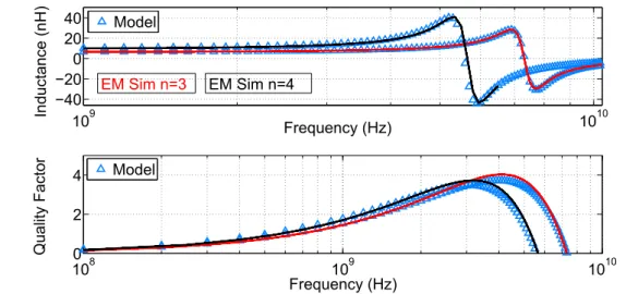
4.4 EM simulation data (solid line) compared with the model for a 3 and 4 turn square inductor in a 0-13µm CMOS technology. . . 49
4.5 EM simulation data (solid line) compared with the model for a 3 and 4 turn hexagonal inductor in a 0-13µm CMOS technology. . . 49
4.6 EM simulation data (solid line) compared with the model for a 3 and 4 turn octagonal inductor in a 0-13µm CMOS technology. . . 50
4.7 Octagonal topology used for simulation in a 0.35-µm CMOS Technology. . 50
4.8 Inductor count over the different error intervals for the inductance value at 100 kHz. . . 52
4.9 Inductor count over the different error intervals for the quality factor, in its peak value. . . 52
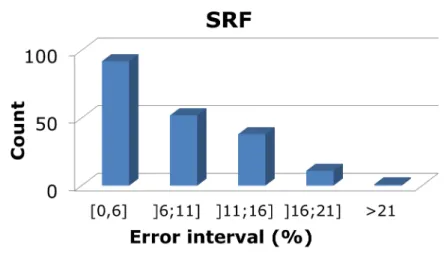
4.10 Inductor count over the different error intervals for the SRF. . . 52
4.11 Square tapered integrated inductor. . . 53
LIST OF FIGURES xv
4.13 Octagonal tapered topology used for simulation in a 0.35-µm CMOS Tech-nology. . . 56 4.14 Two turn inductor values over the different physical parameters for the
quality factor peak value. . . 57 4.15 Two turn inductor values over the different physical parameters for the
inductance value at 100 kHz. . . 58 4.16 Two turn inductor values over the different physical parameters for the
SRF value. . . 58 4.17 Three turn inductor errors over the different physical parameters for the
quality factor peak value. . . 60 4.18 Three turn inductor errors over the different physical parameters for the
inductance value at 100 kHz. . . 60 4.19 Three turn inductor errors over the different physical parameters for the
SRF value. . . 60 4.20 Four turn inductor errors over the different physical parameters for the
quality factor peak value. . . 61 4.21 Four turn inductor errors over the different physical parameters for the
inductance value at 100 kHz. . . 62 4.22 Four turn inductor errors over the different physical parameters for the
SRF value. . . 62 4.23 Five turn inductor errors over the different physical parameters for the
quality factor peak value. . . 64 4.24 Five turn inductor errors over the different physical parameters for the
inductance value at 100 kHz. . . 64 4.25 Five turn inductor errors over the different physical parameters for the SRF
value. . . 64 4.26 Six turn inductor errors over the different physical parameters for the
qual-ity factor peak value. . . 65 4.27 Six turn inductor errors over the different physical parameters for the
in-ductance value at 100 kHz. . . 65 4.28 Six turn inductor errors over the different physical parameters for the SRF
value. . . 66 5.1 EM simulation data (red solid line) compared with the model with the
fitting factors for adjusting the SRF value in a 0.35-µm CMOS technology. 68 5.2 Inductor count over the different error intervals for the inductance value
at 100 kHz. . . 68 5.3 Inductor count over the different error intervals for the quality factor, in its
5.5 EM simulation data (red solid line) compared with the model, for adjusting the quality factor curve in a 0.35-µm CMOS technology. . . 69 5.6 DE algorithm. . . 71 5.7 EM simulation data (solid line) compared with the model for an optimized
1 nH inductor in a 0-35µm CMOS technology. . . 72 5.8 EM simulation data (solid line) compared with the model for an optimized
2 nH inductor in a 0-35µm CMOS technology. . . 73 5.9 EM simulation data (solid line) compared with the model for an optimized
3 nH inductor in a 0-35µm CMOS technology. . . 73 5.10 EM simulation data (solid line) compared with the model for an optimized
4 nH inductor in a 0-35µm CMOS technology. . . 74 5.11 EM simulation data (solid line) compared with the model for an optimized
5 nH inductor in a 0-35µm CMOS technology. . . 74 5.12 Multi-objective optimization with the objective maximizing inductance and
quality factor. Comparison between the model and EM simulations for 40 individuals. . . 76 5.13 First inductor from Table 5.2. Comparison between the model and EM
simulation. . . 78 5.14 Third inductor from Table 5.2. Comparison between the model and EM
simulation. . . 78 5.15 Fifteenth inductor from Table 5.2. Comparison between the model and EM
simulation. . . 79 5.16 Comparison between the optimization carried out with the model, EM
simulation and the inductors generated with the model and simulated electromagnetically. . . 79 5.17 Design flow used in order to reduce the design time. . . 80 5.18 Multi-objective optimization with the objective maximizing inductance and
quality factor. Model simulation for 1000 individuals. . . 81 5.19 Multi-objective optimization with the objective of minimizing the area and
maximizing inductance and quality factor. Comparison between the model and EM simulations for 40 individuals. . . 82 5.20 Multi-objective optimization with the objective of minimizing the area and
List of Tables
3.1 Coefficients for modified Wheeler expression. . . 36 3.2 Coefficients for current sheet expression. . . 36 3.3 Coefficients for data fitted monomial expression. . . 36 4.1 Lsvalue comparison. The inductors have an area of 340×340um2. . . . 46
4.2 Lsvalue comparison. The inductors have an area of 290×290um2. . . . 47
4.3 SRF in GHz andQvalues for the proposed model. ASITIC and EM ADS Momentum simulations in a 0.13-µm CMOS Technology. . . 49 4.4 Geometrical variable ranges for the inductors parameters generated with
LHS. . . 51 4.5 Restrictions on the inductors parameters for comparison with the model. 51 4.6 Lsvalue comparison for a tapered width square layout. The physical
pa-rameters are given inum . . . 54 4.7 Square taperedLsresults for the proposed model comparing with ASITIC
and EM ADS Momentum simulations. . . 54 4.8 Square tapered SRF andQvalues for the proposed model. ASITIC and EM
ADS Momentum simulations. . . 55 4.9 Square taperedLs results for the proposed model. ASITIC and EM ADS
Momentum simulations. . . 55 4.10 Square tapered SRF andQvalues for the proposed model and the
compar-isons with ASITIC and EM ADS Momentum simulations. . . 56 4.11 Physical parameters of the simulated octagonal inductors with two turns. 57 4.12 Two turn octagonal tapered SRF andQvalues for the proposed model and
the comparisons with EM ADS Momentum simulations. . . 57 4.13 Physical parameters of the simulated octagonal inductors with three turns. 59 4.14 Three turn octagonal tapered SRF and Q values for the proposed model
4.16 Four turn octagonal tapered SRF andQvalues for the proposed model and the comparisons with EM ADS Momentum simulations. . . 61 4.17 Physical parameters of the simulated octagonal inductors with five turns. 63 4.18 Five turn octagonal tapered SRF andQvalues for the proposed model and
the comparisons with EM ADS Momentum simulations. . . 63 4.19 Physical parameters of the simulated octagonal inductors with six turns. . 63 4.20 Six turn octagonal tapered SRF andQvalues for the proposed model and
the comparisons with EM ADS Momentum simulations. . . 65 5.1 Comparison between the inductance and quality factor value for the
opti-mized inductors. . . 72 5.2 Inductors physical parameters and comparison between the inductance
Abbreviations
VCO VoltageControlledOscillator LNA LowNoiseAmplifier
RF RadioFrequency
CMOS ComplementaryMetal-Oxide-Semiconductor DC DirectCurrent
IC IntegratedCircuit SoC SystemonChip EM Electromagnetic
SRF Self-RessonanceFrequency
MMIC MonolithicMicrowaveIntegratedCircuit GaAs GalliumArsenide
PGS PatternedGroundShield SGS SolidGroundShield
1
Introduction
The beauty of wireless connections through radio frequency (RF), for both voice com-munications and data transmission, has been motivating research work in this field ever since Guglielmo Marconi sent the first radio signal across the Atlantic ocean in 1901 [14]. At the time the motivation was the ability to communicate with people at hundreds of kilometres away. Nowadays, the ability to communicate with people is taken for granted, and the main goal is now to increase the amount of information sent. To accomplish this goal, an increasing demand for bandwidth has pushed new standards in the wireless do-main. These new standards evolved towards higher operating frequencies. Besides the importance of the increase of the bandwidth, wireless transmission allows the elimina-tion of a physical connecelimina-tion between receiver and transmitter, which is a key advantage in modern communication systems.
1.1
Background and Motivation
on-chip inductors, which nowadays are a key component in radio frequency, where they are used in tuning, filtering and impedance matching applications.
There are only a few options when integrating inductors, such as on-chip inductors are bond wires and planar spiral geometries. For simulating the inductor performances, there are mainly two options when designing inductors, electromagnetic (EM) simula-tions or analytical models, either physical or surrogate. While, EM simulasimula-tions are ac-curate but time consuming, the already developed models are not sufficiently acac-curate. The objective of this thesis is to develop a model which is suitable to design spiral inte-grated inductors of any shape (such as square, hexagonal or octagonal). This model is to be integrated into optimization processes.
1.2
Thesis Outline
The outline of this thesis is as follows. Chapter 2 introduces the basic principles of in-tegrated inductors, such as its physical parameters. Some important effects such as the self-resonance frequency will be introduced and the losses associated with integrated in-ductors will be briefly explained. A revision of the most important lumped-element mod-els reported in the literature for integrated inductors will also be presented. Advanced structures for integrated inductors will be presented, that reduce the losses associated to the simplest integration techniques.
Chapter 3 the model developed in this thesis is presented. The chapter starts by in-troducing the segmented model, which is the main feature of the model used. Then the chapter introduces the analytical expressions of the model to calculate resistances and ca-pacitors and how to evaluate the inductance of any type of integrated inductor topology. Chapter 4 validates the model for two different technologies against field solvers, ASITIC and electromagnetic simulations. Firstly the inductance model is validated in a 0.13µm CMOS technology against ASITIC and afterwards the model is validated for three different layouts, square, hexagonal and octagonal, with all the inductors having equal turn widths. The model is also validated in a 0.35 µm CMOS technology for an equal turn width octagonal layout. In this case a statistical study was performed with 1000 inductors generated with the latin hypercube sampling technique. The capabillity of the model was also tested for inductors with variable turn widths, commonly denomi-nated tapered width inductors. Again, the inductance model is validated against ASITIC for square layouts. Afterwards an extensive study is made for octagonal tapered width inductors, in order to understand how does the inductors quality factor improve with the tapered width technique.
1. INTRODUCTION 1.3. Thesis Contributions
information about the entire design space for a given technology. All the optimizations are done with a 0.35µm CMOS technology. Conclusions to this work are drawn out in chapter 6 together with future work.
1.3
Thesis Contributions
The work developed in this thesis provided the means to improve the existing literature about the modeling of integrated inductor. This thesis originated six different publica-tions into several different well known international conferences and journals.
1. The first publication, Analythical Characterization of Variable Width Integrated Spiral Inductors, on the 20th IEEE MIXDES Conference, introduces the model and explains how to accurately calculate the inductance parameter of several inductor topolo-gies. This paper was given theOutstanding Paper Awardon that conference.
2. The second publication, A Wideband Lumped-Element Model for Arbitrarily Shaped Integrated Inductors on the 21st IEEE ECCTD Conference, introduced the complete model and its validation is made against EM simulations for a 0.13µm CMOS tech-nology.
3. The third publication on the 28th DCIS conference is entitled,A Wideband Lumped-Element Model for Integrated Spiral Inductors, and shows the ability of the model to design tapered inductors.
4. The fourth publication, on the IEEE COMCAS 2013, shows a statistical study over an high number of inductors, providing therefore a better understanding over the range of geometrical parameters where the model shows accurate results.
5. The fifth publication, on the DoCEIS 2014, shows results for the single-optimization processes.
2
Planar Spiral Integrated Inductors
In this second chapter the basic theory about integrated inductors design will be pre-sented. Afterwards some insights about integrated inductors modelling techniques, such as electromagnetic simulations or lumped element circuits used to characterize inductors will be presented. Special emphasis is given to the well knowπ-mode and the2π-model. Finally, advanced structures developed in order to minimize effects that negatively af-fect the performances of the inductor, such as the series resistance or the capacitances between the metal and the substrate, will be described.
2.1
Integrated Spiral Inductor Basic Insights
2.1.1 Integrated Inductor Geometries and Basic Topologies
Integrated inductors are usually fabricated using the outer metal layers of the standard CMOS processes. This is done to avoid coupling effects with the substrate. Some pro-cesses offer the possibility to use a thicker metal layer that allows a reduction of the resistivity of the metal. The basic structure of an integrated inductor is made up of one or more metal tracks in parallel forming one or several concentric turns, requiring a min-imum of two metal layers and one via connection between them for inductors with 2 or more turns. In order to design an inductor it is important to consider both the vertical and lateral geometries of the layout. In Fig. 2.1 it is possible to observe a three dimensional square spiral inductor.
Figure 2.1: 3-D view of a square spiral inductor [1].
polygonal with many sides. Fig. 2.2, Fig. 2.3, Fig 2.4 and Fig. 2.5 show the different layouts, for square, hexagonal, octagonal and circular respectively.
Figure 2.2: Square spiral inductor [1].
Figure 2.3: Hexagonal spiral inductor [1].
The geometry of a planar spiral inductor is defined by five geometric parameters: 1. number of turns,n,
2. metal width,w,
3. spacing between turns,s,
4. any of the following: the outer diameterDoutor the inner diameterDin,
5. number of sides,N.
2. PLANARSPIRALINTEGRATEDINDUCTORS 2.1. Integrated Spiral Inductor Basic Insights
Figure 2.4: Octagonal spiral inductor [1].
Figure 2.5: Circular spiral inductor [1].
lateral and vertical dimensions are used to define the other two important performance parameters, Q and SRF, as it will be explained afterwards. In Fig. 2.6, a typical cross section of an inductor is presented.
Integrated planar inductors can be defined by a simple model at low frequencies (ne-glecting parasitic capacitances) as shown in the Fig. 2.7.
For these conditions, the input equivalent impedance can be written as follows:
Zeq=Rs+jωLs (2.1)
whereRsandLsare the series resistance due to the conductivity of metal and the
induc-tance of the component, respectively. A physical interpretation of both parameters will be discussed later.
2.1.2 Inductance
Inductance, Ls, is the relationship between the total current flow through the spirals
and the magnetic field generated by this current. The relationship between the self-inductance L of an electrical circuit in Henry, given by,
v=L·di
dt (2.2)
Figure 2.6: Vertical cross section of a square spiral [1].
Ls
Rs
Figure 2.7: Simple model of inductor at low frequency.
change of the current through it. All integrated conductors have some inductance, which may provide either beneficial or detrimental effects. There are three types of inductances, as it can be seen in the following equation,
Ls=L0+LM++LM− (2.3)
where:
• Lsis the total inductance of the inductor.
• L0 is the auto inductance associated to each coil.
• LM+is the mutual inductance between the coils where the direction of the current
flow generates magnetic fields lines in the positive direction.
• LM−is the mutual inductance between the coils where the direction of the current flow generates magnetic fields lines in the negative direction.
Another method and possibly the more general method to obtain the equivalent induc-tance of planar inductors is from the equivalent impedance, shown in equation 2.4.
Ls=
Im(Zeq)
2. PLANARSPIRALINTEGRATEDINDUCTORS 2.1. Integrated Spiral Inductor Basic Insights
2.1.3 Quality Factor
The quality factor,Q, is an extremely important figure of merit when designing a inte-grated inductor. Basically, it describes how good an inductor works as an energy-storage element. In the ideal case, inductance is pure energy-storage element (Qapproaches in-finity), while in reality, parasitic resistances and capacitances reduce the value ofQ. This is caused by the fact that parasitic resistance consumes stored energy, and the parasitic capacitance reduces inductance (the inductor even turns capacitive at high frequencies. Several different definitions of quality factors for inductors have been used in the litera-ture [2]. The most general definition forQ-factor is given by Eq. 2.5,
Q= 2π· Estored
Edissipated (2.5)
where Estored is the energy stored in the passive component, whereas Edissipated is the
energy loss in one cycle. A good approximation to understand what the quality factor means in to think thatQ-factor is a measure of the ratio of the desired quantity of induc-tance to the undesired quantity of resisinduc-tance. Another equation, which is widely used for calculate the inductor quality factor is therefore given by,
Q= Im(Zind)
Re(Zind) (2.6)
whereZindis the impedance of the inductor.
2.1.4 Self-Resonance
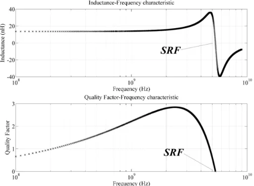
At low frequencies, the inductance of an integrated inductor will be relatively constant, and this zone is called by some authors the flat-bandwidth region [15]. The inductor should work in this flat-bandwidth zone, where the inductance value has not changed much from DC value and the quality factor is near its peak, but with a positive slope. When the operating frequency increases, the effect of parasitic capacitances start to in-crease and the inductance value is no longer constant. Finally, at one frequency point, the admittance of the parasitic capacitances will cancel the inductance of the inductor and it stops behaving as an inductance source and will act as a purely resistive load to the circuit. The point in frequency where this phenomenon happens, is called the self-resonance frequency (SRF). At this point the inductance,L, is equal to zero, which also brings the quality factor to zero. This phenomenon can the observed in Fig. 2.8, where a typical integrated inductor characteristics is presented.
Figure 2.8: Self-Resonance frequency shown both in inductance-frequency graph and quality factor-frequency plots.
2.1.5 Losses in Integrated Inductors
There are several mechanisms and effects that can produce losses in integrated induc-tors. The most common and most significant losses are conductive losses, which are related with the resistance of the metal lines. Integrated inductors are further affected by the internally induced losses, which are caused by the increase of frequency and temper-ature. As the frequency and temperature raises, the resistance of the metal lines show a significant growth, which leads to more losses.
The externally induced losses, are another problem that affects integrated inductors in silicon substrates. This losses are created by a time-varying flux which creates a phe-nomenon called Eddy currents. Integrated inductors also have the so called magnetiza-tion losses, which are related to the fact that for magnetic materials, the magnetic perme-abilityµis non-linear and frequency dependent and dissipative [16].
As previously said, a spiral is usually implemented in the topmost available metal, because of its low resistivity and lower parasitic capacitances to substrate. In sub-micron CMOS technologies, the top metal layer has the largest thickness, thereby minimizing the DC series resistance of the inductor. Due to the large variety ofSi technologies and
2. PLANARSPIRALINTEGRATEDINDUCTORS 2.1. Integrated Spiral Inductor Basic Insights
and losses are discussed in the following sections.
2.1.5.1 Sheet Resistance and Skin Depth
The sheet resistance arises from the resistivity of the metal. At low frequencies, the resis-tance of the inductor is given by Eq. 2.7,
RDC =
l·ρ
w·t (2.7)
wherelis the conductor length,ρis the resistivity of the material, wis the metal width andtthe metal thickness. However, at high frequencies, another effect comes into play. Electromagnetic waves suffer attenuation as they enter a conductor. As the frequency approaches the GHz range, the distance that the waves can penetrate becomes compa-rable to the size of the metal line. The problem is that the current becomes concentrated around the outside of the conductor, with much less current flowing in the center of the conductor. This effect is shown in Fig. 2.9, where the current concentration is defined by the colour red. This is known as skin effect, and can be explained by the tendency of an alternating electric current (AC) to become distributed within a conductor such that the current density is largest near the surface of the conductor, and starts decreasing into the center. The electric current flows mainly at the "skin" of the conductor, between the outer surface and a level called the skin depth. The skin effect causes the effective resistance of the conductor to increase at higher frequencies where the skin depth is smaller, thus reducing the effective cross-section of the conductor.
Figure 2.9: Skin depth definition through a circular conductor.
The skin depth,δ, is given by the following equation [17],
δ = r ρ
πf µ (2.8)
wheref is the frequency andµis the permeability of the metal. Due to this effect the series resistance of an inductor is commonly stated as follows [17],
Rrf =
l·ρ
wheretef f is given by Eq. 2.10 [17].
tef f = (1−e−t/δ) (2.10)
The DC sheet resistance of a spiral coil can be reduced by using a thicker metallization. Several thin metal layers can be connected or shunted together to realize a thick metal layer and therefore reduce the sheet resistance. Alternatively, high-conductivity conduc-tors such as copper or gold can be used instead of the aluminium, which is by far the most commonly used inSi technologies [18]. AdvancedSi technologies (bothSi CMOS
andSiGeBiCMOS) have a very thick copper interconnection layer as the last metal. With
these technologies inductorQ-factors can easily approach those typically found on semi-insulating substrates [2]
2.1.5.2 Eddy Currents
Eddy currents are electric currents that appear in the inner turns of the integrated induc-tors created by a changing magnetic field in the conductor. These circulating currents have inductance and thus induce magnetic fields. These fields can cause repulsive, at-tractive, heating effects among others [2]. Consider a n-turn spiral inductor as shown in Fig. 2.10. The currentIcoilis the induced current, which has an associated magnetic flux,
Bcoil. The magnetic flux lines enter the page plane at the far end of the turnnand come
out of the page plane in the center of the coil, where they have maximum intensity. When there is not enough hollow space in the center of the coil, a large part of the magnetic flux also goes through the inner turns.
According to Faraday-Lenz’s law, when a conductor is moved into a magnetic field or a conductor is placed in a time-varying magnetic field, eddy currents are induced in the conductor in the direction where their self-flux is opposite to the applied magnetic field. Thus, as shown in Fig. 2.10, circular eddy currentsIeddy are generated due to
mag-netic fields that go through the inner turns, and an opposing magmag-netic field,Beddy, due
to eddy currents is established. The eddy current loops produced within the trace width cause non-uniform current to flow in the inner coil turns. Because this eddy currents are induced due to time-varying magnetic fields, their values are a strong function of frequency, and it is possible to estimate the critical frequency at which this effects start being significant. The critical frequency fc at which the current crowding begins to
be-come significant is given by [2],
fc=
3.1·(w+s)
2π·µ·w2 ·Rsh (2.11)
2. PLANARSPIRALINTEGRATEDINDUCTORS 2.2. Integrated Spiral Inductor Modelling
Figure 2.10: Excitation and eddy currents, and fields in a coil.Icoilis the excitation current
[2].
2.1.5.3 Magnetic Losses
In heavily dopedSisubstrates, currents induced by the penetration of the magnetic fields
into the substrate cause extra resistive loss. Consider Fig. 2.11, which shows magnetic field flux lines associated with the coil excitation current. The flux lines uniformly sur-round the inductor and penetrate into the substrate. As discussed above, due to the Faraday-Lenz law, loops of eddy currents flow in the low-resistivity substrate underneath the coil, with higher current density closer to the coil. The direction ofIsubis opposite
to the direction ofIcoil, giving rise to extra substrate loss. Because this loss is associated
with magnetic fields, it is commonly referred to as magnetic or inductive substrate loss. Substrates with high resistivity have negligible magnetic loss. In summary, by using nar-row conductors that meet skin effect requirements (w≃3d) in the inner turns, using a hollow coil design, and using compact area coils, one can keep the substrate loss to a min-imum. Because the magnetic field in a small coil penetrates less deeply into the substrate, eddy current loss is not as severe as for large coils. Therefore, an optimum solution, in terms of inside dimensions and coil area for a given substrate, can be found.
2.2
Integrated Spiral Inductor Modelling
Figure 2.11: Currents and fields in a coil printed on a lossySisubstrate [2].
discussed.
2.2.1 EM Simulations and Field Solvers
Electromagnetic field solvers, commonly called field solvers, are specialized programs that solve Maxwell’s equations directly. There are several 3-D electromagnetic simu-lators that solve Maxwell’s equations numerically, such as ADS Momentum, M axwell, EM-Sonnet andM agN et [19] [20] [21]. Although accurate, these simulators are com-putationally intensive, both in memory and time. Thus, while these field solvers are suitable for accurately simulating simple structures, they are not suitable for simulating large three dimensional structures with multiple segments.
2. PLANARSPIRALINTEGRATEDINDUCTORS 2.2. Integrated Spiral Inductor Modelling
simulators such as SPIRAL and ASITIC [22] are available. However the use of these tools complicates the interface between the inductor model and the circuit simulator (such as SPICE). The best way to incorporate these field solvers in the design flow is to use them first to generate a library of inductors that span a wide design space and then link that library to the circuit simulator. Unfortunately, this requires new libraries to be generated for every process or, worse, an existing library to be updated even if only a few process parameters are changed [1]. Due to the previous reasons, field solvers are best suited to verify results rather than design and optimize integrated inductor circuits.
2.2.2 Lumped Element Circuit Models
The disadvantages of the 3-D EM simulations indicate the need for a model that can be incorporated into a spice like simulator, in order to reduce the simulation time. Signif-icant work has gone into modelling spiral integrated inductors using lumped element circuits. This section will present state-of-the-art modelling of inductors through lumped element circuit models.
The first lumped element circuit used to model a spiral inductor was a RLC circuit in 1980 [3]. Even though the authors were considering the work to be used in air core inductors for high power, DC-DC conversion circuits, this model, shown in Fig. 2.12, was the starting point for all the following ones.
Figure 2.12: First RLC circuit used to model an integrated inductor.
Four years later, a MMIC spiral inductor was modelled with aπ circuit in [23], like shown in Fig. 2.13. The name π circuit, adcomes from the fact that the circuit looks like the greek letterπ. Normally theLs andRs are called the series branch whereas the
capacitance to the ground is called the shunt branch.
Figure 2.13: Firstπmodel used to model an integrated inductor.
In 1985 [24], microstrip spirals were modelled with aπcircuit that used a capacitance in parallel with the series branch. This equivalent circuit is shown in Fig. 2.14 [25].
Figure 2.14: Firstπmodel that utilized the RLC branch from [3].
was developed in the context of GaAs MMICs [25] ans the circuit is shown in Fig. 2.15
Figure 2.15: Firstπmodel with a resistor to model the leakage current.
In 1989, an effort was made to extend the frequency range of theπmodel by increasing the complexity of the model. This new model blocked the DC leakage current to ground by replacing the shunt branches with a series RC pair [27]. In 1994, the first model was improved to the circuit presented in Fig. 2.16. This would became the most common spiral inductor model for silicon processes. It has the now common RLC triple in its series branch, its shunt branches have a DC blocking capacitor in series with a parallel RC pair [28].
Many authors have attempted to find empirical formulas to extract the component values in the extracted model from the physical properties of the spiral inductor [29] [30]. However this model presents a problem reported in several published works, which is the need to increase the viable bandwidth of usage [25]. In [31], for example, Rs is
2. PLANARSPIRALINTEGRATEDINDUCTORS 2.2. Integrated Spiral Inductor Modelling
Figure 2.16: Commonπmodel for silicon substrates.
Figure 2.17:πmodel for silicon substrates with leakage current resistor.
In 1997, Yorgos K. Koutsoyannopoulos, proposed a model which is the starting point for this thesis. The model divided the inductor into segments and then considered the self and mutual inductance of each segment [34] [35]. This model will be explained in detail in section 3.1. In 2002, [36] and [37], introduced the so called skin effect model, as shown in Fig. 2.19. This would become very common and it is a variant of the simpleπ model, in addition it had a parallel RL branch in series with theLsandRs.
Figure 2.18: Doubleπmodel for silicon substrates.
Figure 2.19:πmodel for silicon substrates considering the skin effect.
series RL connected in parallel with the resistor in the series branch.
In Fig. 2.20, a complex model is presented. This model was proposed in [41]. This model would also go on to become rather popular [25]. It is meant to include skin-effect, proximity effects and the substrate conductivity in a twenty-two element topology with two mutual inductances. Some authors also proposed simpler methods for extracting the component values, for example, Kim, Han and Liu present the extraction of the com-ponents through the admittance parameters [42]. In [43] two and three port, doubleπ, skin-effect models are presented and in [44] some additional elements were added to the simple π model, but they are considered "without any physical meaning". A new ap-proach came in 2003, when [45] outlined the use of a modified T instead of a π model. The author also approached the problem from a new perspective by starting with a mod-ified T model normally used to model transmission lines. This transmission line equiva-lent Modified T model is then developed into one that proves to be a suitable wideband model for spiral inductors for LTCC, this model is shown in Fig. 2.21.
2. PLANARSPIRALINTEGRATEDINDUCTORS 2.2. Integrated Spiral Inductor Modelling
Figure 2.20: The complex model.
a starting point, [47] took the work further by replacing inductors in the series branches with ideal transmission lines and associating each Simple Model with a single turn of the spiral inductor. In [48], Scuderi, Biondi, Ragonese, and Palmisano, presented an "Improved π" topology that is able to model the spiral inductor beyond its Self Reso-nance Frequency (SRF), which at the time was a improvement into integrated inductor modelling. Xiong and Rustagi introduced a modified version of theπ Model in [49] for multi-level spirals. In this work the series branch is modelled with inductively coupled series RL pairs, connected to each other through parallel RC pairs. In March 2003, [50] maintained the simplicity of theπModel by adding a single inductively coupled RL pair to model eddy currents in silicon. In June of the same year, [51] presented the double π version of the same model. It also described the branches of the double π being ex-tracted independently from one another. In December 2003, [52] introduced one of the first asymmetric spiral models. This model is for stacked RFIC spirals and is based on the doubleπvariant of theπmodel. In the same month, [53] introduced the N-pi version of [52]. The version in [53] uses so-called "N-cells" to model the turns of the spiral. Fig. 2.22 illustrates this topology.
Reference [54] introduced the most complex model presented so far. It is meant to model a three-port differential inductor in aSiGe HBT technology. A modified double
Figure 2.21: Modified T spiral inductor model.
Figure 2.22: Three nested "N-Cells" spiral inductor model.
2. PLANARSPIRALINTEGRATEDINDUCTORS 2.3. Integrated Inductor Advanced Structures
in [69]. In 2010, a skin-effect model was modified with inductors in the shunt branch. These inductors are coupled to the main inductor in the series branch. An extraction method is provided and the model is shown to work well beyond the SRF.
Despite all the presented models that have already proven its validity, the model developed in this work is based on the basic π model, shown in Fig. 2.16 and based on the work presented on [34] [35]. The objective of this thesis, is to develop a model that is suitable to be used for arbitrary shaped integrated inductors with equal of non-equal turn widths. So this reduces the models that can be used, because the model can only be defined by one series branch, as it will be explained further on. Also, a good complexity-simplicity relationship is desired, so theπmodel suits the work. It is known that this model has some limitations, that are discussed after the detailed presentation of the model, in Section 3.4.
2.3
Integrated Inductor Advanced Structures
The design of an optimal spiral is highly frequency dependent. This is due to the multiple loss mechanisms that appear from the distributed effects in the structure. In general, for a fixed area, we can design an inductor with many different values of metal widthw, spacings, and turnsn, to achieve the same value of inductance. As we increasew for instance, the resistance drops. The substrate losses, though, tend to increase with w, since the increase ofw, increases the capacitance of the structure. At the same time, we observe that structures with more turns,n, tend to have higher resistive losses in the inner turns. Besides the effects that geometrical parameters have in the behaviour of integrated inductors, the performance of a typical integrated inductor can be improved with several advanced structures developed through time. Some of these structures are explained in the following sections.
2.3.1 Structures to Reduce Substrate Loss
2.3.1.1 Patterned Ground Shield (PGS)
The substrate loss can be reduced by decreasing the substrate resistanceRsub. To achieve
this, one can insert a metal or poly-Si(polycrystalline silicon) layer between the inductor
and substrate, and connect this layer to the ground. This approach, called the ground shielding, reduces the effective distance between the spiral metal and ground and thereby reduces the substrate coupling resistance. For a solid ground shield (SGS), however, the varying electromagnetic field in the inductor could induce the eddy current with the presence of ground plane, and the reflected image in the ground plane serves as a counteractive inductor [70]. So it is necessary to pattern the shield as shown in Fig. 2.23 to cut the eddy current loop.
It has been reported that poly-Si is a good material for the patterned ground shield
(a) Substrate with patterned ground shield.
(b) Inductor in a patterned ground shield.
Figure 2.23: Patterned Ground Shield (PGS).
Figure 2.24: Quality factors of solid ground shield (SGS), PGS, and no ground shield (NGS) [4]
shield improves the quality factor in a considerably scale. Since the substrate current mainly concentrates at theSi-SiO2 surface due to the proximity effect, the PGS can
2. PLANARSPIRALINTEGRATEDINDUCTORS 2.3. Integrated Inductor Advanced Structures
(a) Topology of a suspended inductor.
(b) Comparison of inductances and Q factors of conven-tional and suspended inductors.
Figure 2.25: Suspended Inductor [5].
2.3.1.2 Substrate Removal
Besides the PGS there is another way to enhanceQ, which is to theoretically increase the substrate resistance toinf inite. A possibility to do this is to use a insulator as substrate. Quartz or glass have proven to achieve betterQand higher self-resonant frequency than Sisubstrates [73]. ForSitechnology, however, it is not possible to use a high resistive
sub-strate as an effective radio frequency (RF) ground [18]. In other words, for CMOS-based on-chip inductors, it is impossible not to use a low resistiveSi substrate. Nonetheless,
(a) Topology of a microma-chined inductor.
(b) Q factors of micromachined inductors with two dif-ferent diameters.
Figure 2.26: Micromachined inductor [6].
(a) Inductor with substrate removed by a deep trench technology.
(b) Q factors of conventional and trenched inductors.
2. PLANARSPIRALINTEGRATEDINDUCTORS 2.3. Integrated Inductor Advanced Structures
2.3.1.3 Horizontal Inductors
Another way to reduce the substrate losses is to reduce the magnetic field coupling to substrate. This can be obtained by having the magnetic field parallel to the substrate. Research works have been studying the possibility to fabricate horizontal inductors with multilayer interconnections [76] [77]. By using this technique, the magnetic field is paral-lel to the substrate surface and the magnetic coupling to the substrate is minimal. How-ever this structure increases the coupling capacitance. Since a large metal is needed for the bottom layer of the horizontal inductor, the inductor-substrate capacitance increases tremendously if the inductor is on silicon. Again, researchers tried to use high resistive substrate [77], and suspended the inductor in air [78], or even rectify the inductor with the so-called plastic deformation magnetic assembly (PDMA) [8]. Fig. 2.28 shows the topology and performance of a horizontal inductor using the PDMA.
(a) Topology of the horizontal inductor based on the PDMA process.
(b) Q factors of conventional and horizontal inductors.
2.3.2 Structures to Increase Inductance
Since the quality factor is directly proportional to the series inductance, approaches to increase the inductance have also been suggested for on-chip inductor performance en-hancement.
2.3.2.1 Stacked Inductor
A stacked inductor is a set of series inductors made from different metal layers, as illus-trated in Fig. 2.29. This method maximizes the inductance per unit area. It has been reported that a 10 nH inductor can be achieved with an area of 22 µm2 ∼ 23 µm2, as
opposed to several hundredsµm2
for regular inductors [9]. This is the main advantage that this technology can offer. The biggest drawbacks are the relatively lowQfactor and self-resonant frequency, due to the increase of the substrate capacitance and line to line coupling capacitance. TheQfactor and inductance of such an inductor are illustrated in Fig. 2.29.
(a) Stacked inductor with six metal layers.
(b) Qfactors of conventional and horizontal inductors.
Figure 2.29:Qfactor and inductance of the stacked inductor [9].
2.3.2.2 Miniature 3-D Inductor
2. PLANARSPIRALINTEGRATEDINDUCTORS 2.3. Integrated Inductor Advanced Structures
(a) Structure of the miniature 3-D in-ductor.
(b) Capacitances of typical stacked and 3-D induc-tors,.
(c)Qfactors of typical stacked and 3-D inductors.
2.3.3 Structures to Reduce Series Resistance
Metal resistivity gives rise to the series resistanceRs, and it is always desired to reduce
the resistance in order to improve the quality factor. One simple idea is to increase the line width. This method may work at low frequencies where the current density in a wire is uniform; however, as the frequency increases, the skin effect pushes more current to the outer cross section of the metal wire and the so-called skin depth (i.e., the depth in which the current flows) is reduced with increasing frequency (see Eq. 2.8). Thus, the skin effect increases the series resistance at high frequencies, and the approach of increasing the line width would not be effective. According to an earlier study, the larger the cross section, the lower the onset frequency at which the skin effect dominates the series resistance. Furthermore, a wider metal line would occupy more area, which increases the fabrication cost. Several possible solutions to this problem are given below.
2.3.3.1 Vertical Shunt
In this approach, the inductor is made of multiple metal layers and the neighboring metal layers are shunted through via arrays, so the effective thickness of the spiral inductor is increased, the skin effect is weakened, and the series resistance is reduced. A detailed study and comparison on the multilayer inductors are presented in [11].
(a) Inductor with multiple metal layers and vertical shunt.
(b) Maximum Q factors and resistances for the inductor having different numbers of vertical shunt.
2. PLANARSPIRALINTEGRATEDINDUCTORS 2.3. Integrated Inductor Advanced Structures
The inductors are fabricated with multiple metal layers (M1 to M4). These layers can be shunted through via arrays, as shown in Fig. 2.31 for the case of shunting M2, M3 and M4. The results in Fig. 2.31 show a reduced series resistance and thus an im-provedQas the number of shunts is increased (i.e., the case of M3 has no vertical shunt). The performance of the inductor is therefore optimized with the increment of total metal thickness without occupying more area. One important aspect the inductor in Fig. 2.31 did not address is that the inductor may experience a lower self-resonant frequency with the utilization of lower metal layers. This is due to the following effects:
• The reduction of metal-substrate distance could cause a significant increase inCox,
• The capacitance among the metal lines would also increase.
2.3.3.2 Horizontal Shunt
Instead of shunting vertically, the spiral inductor can be split into several shunting cur-rent paths, each with an identical resistance and inductance. This approach, called the horizontal shunt, can suppress the current crowding and increase theQfactor [12]. Figs. 2.32 show such an inductor and itsQfactor. It is shown that for the same line width, the Qfactor increases with increasing number of splits.
(a) Inductor with metal line split into shunt current paths.
(b) Q factors of horizontally shunt inductor with one, two, and three splits in the metal line.
Figure 2.32: Horizontal shunt inductor [12].
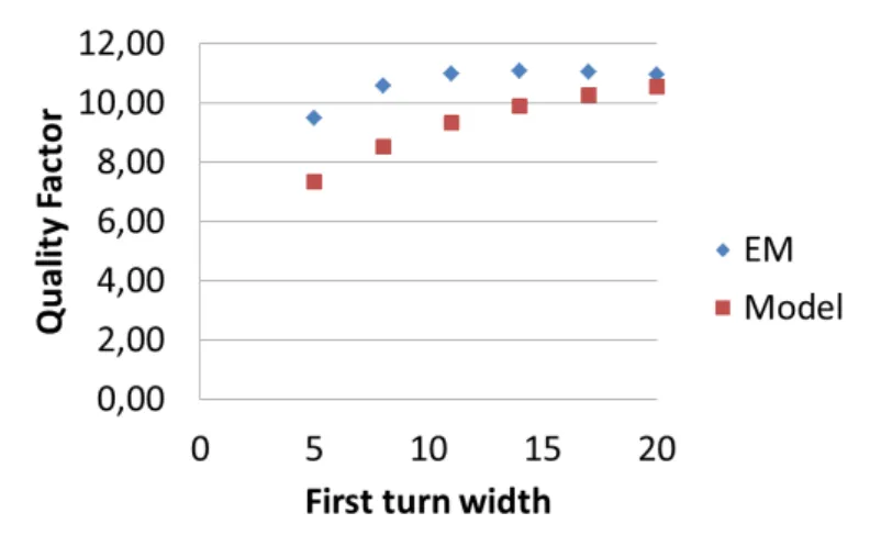
2.3.3.3 Variable Width Inductors
Figure 2.33: A square spiral inductor with tapered trace width.
Figure 2.34: Q factors of a tapered inductor and three non-tapered inductors [13].
performance of the spiral can be improved. Since the wide inner turns do not lower the resistance (due to current constriction), it is better to transfer the width to the outer turns, while keeping the total area of the spiral constant.
Detailed study was performed in [13] regarding the optimization of line width in order to enhance the RF performance. The frequency and position-dependent optimum widthWoptis given by:
Wopt,n =3
s
rs(f)
2·C·g2
n·f2
(2.12) wherers(f)is the sheet resistance of the metal strip,f is the frequency,Cis a fitting
constant, andgnis a geometric dependent parameter. As can be seen in Fig. 23(b), theQ
3
Analytical Modelling of Integrated
Inductors
In this chapter the developed model will be explained. The model is based in the usually called segmented model, due to the fact that the inductors are divided into segments. The analytical expressions for each lumped element will be presented and its physical definition will be given.
3.1
Segmented Model and its Analytical Expressions
Considering a one-turn square inductor, the idea is to divide the inductor into four seg-ments, as shown in Fig. 3.1. Afterwards, a π lumped element circuit is used to model each segment of the integrated inductor. Theπ model, shown in Fig. 2.16, was intro-duced in the previous chapter but a detailed explanation of its elements will be given in this chapter.
Figure 3.1: Inductor model description for a one-turn inductor.
trimming into different segments and afterwards the usage of lumped-elements to char-acterize the inductor. At the final stage of the modelling one should have a circuit like the one shown in Fig. 3.3. For the sake of simplicity, when using a SPICE-like simulator it is possible to sum each one of the lumped element of each segment, this way we will have just one equivalent schematic, which will speed up the inductor design.
Figure 3.2: Model explanation with an inductor trimmed and theπmodel.
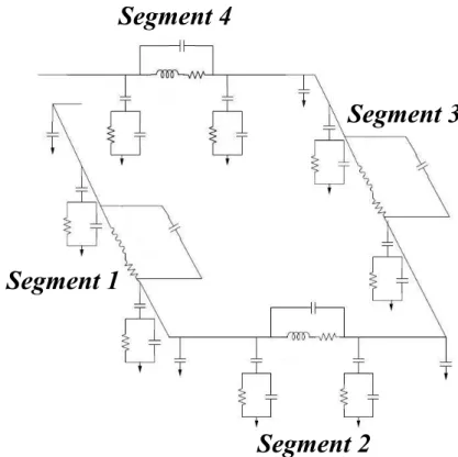
Segment 4
Segment 3
Segment 2
Segment 1
Figure 3.3: One-turn integrated inductor defined by the segment model.
The series branch of this model, consists ofLs,RsandCp. The series resistance,Rs
arises from metal resistivity of the inductor and is closely related to the quality factor, being a key issue for inductor modelling. The series feedforward capacitance, Cp, has
3. ANALYTICALMODELLING OFINTEGRATEDINDUCTORS 3.1. Segmented Model and its Analytical Expressions
Figure 3.4: Physical definition of the lumped-elements of the inductor model.
size of CMOS process continues to shrink, the spacing between metal spirals,s, can be reduced to a value similar to the distance to the underpass. Therefore the coupling ca-pacitance between metal lines,CL, can play a major role in the total capacitance of the
device, and therefore in the self resonance frequency (SRF).Cpis then given by the sum
of Cs andCo. The capacitanceCox represents the oxide capacitance between the spiral
and the substrate. The silicon substrate is modelled withCsubandRsub[80] [30] [81] [18].
Rs=k·
ρ·l
w·δ·(1−e−t/δ) (3.1) Cox=
1
2 ·l·w· εox
tox (3.2)
Rsub=
2
l·w·GSub (3.3)
Csub=
1
2 ·l·w·Cms (3.4)
Co=n·w2·
εox
tM1−M2
(3.5) Eq. 3.1 to Eq. 3.5 define theπ model for an integrated inductor on silicon. However, as it was mentioned previously, with the continuing shrinking size of CMOS and with higher operating frequency, swill get smaller and the parasitic capacitances will affect inductors more significantly. In Eq. 3.1,kis a fitting factor.
To use this model up to higher frequency range, the capacitanceCL must be taken
into account andCoxandCsubshould be calculated using different methods that include
[83]. For the sake of simplicity the following assumptions should be made.
1. The wiring metal width should be much larger than the spacing.
2. Voltage distribution is proportional to the lengths of the metal tracks, i.e., if the metal track is longer, the voltage drop on the track is higher.
3. In the same turn, the voltage is regarded as constant and it is determined by aver-aging the beginning voltage and the ending voltage of the turn.
To calculate the capacitances, we first define the lengths of each segment asl1, l2,...,
ln, and the total length asltot=l1+l2+...+ln, wherelnis the length of the last segment of the
outer turn. Afterwards we define,
hk= n
X
k=1
lk
ltot (3.6)
and the capacitances can be calculated with the following formulas [82],
Cs = n
X
k=1
x · 4
3Cmmlk ·
(hk−hk−1)
2+ (h
k+1−hk)2+ (hk+1−hk)(hk−hk−1) (hk+1−hk−1)
2 (3.7)
Cox = n
X
k=1
x · 1
2 · 4
3Cmslk ·
(1−hk−1)
2+ (1−h
k)2+ (1−hk)(1−hk−1) 3(2−hk−hk−1)
2 (3.8)
An empirical scale factorx, which is the same for both equations, of the totalCp
ca-pacitance for each segment is shown to match the distributed caca-pacitance for simulations over a wide range of physical parameters and layouts. This empirical capacitance fac-tor is then used as a fitting parameter to the measured SRF and Q over a large set of inductors.
The 1/2 factor inCox, is due to the fact that the capacitance is divided into two in the
π-model. Cmm andCms, are the unit length capacitance between the metal spirals and
the unit length capacitance between the metal and the substrate, respectively. Normally these are extracted from measured data, but they can be approximated as follows [84],
Cmm =
ε0εsiO2·t
s (3.9)
Cms=
ε0εsiO2·w hsiO2
3. ANALYTICALMODELLING OFINTEGRATEDINDUCTORS 3.1. Segmented Model and its Analytical Expressions
The substrate resistance is crucial for accurately modelling of the peak Q and the shape of theQcurve, along with the series resistanceRs. This resistance can be calculated
by Eq. 3.11, given in [18] and [30],
Rsub=
2
l·w·Gsub (3.11)
wherel is the segment length andGsub is the conductance per unit area for the silicon
substrate and can be approximated according to [84] by,
Gsub=
σsi
hSi
(3.12) whereσSi is the conductivity of the silicon substrate andhSi is the thickness of the
sub-strate.
The substrate capacitance can normally be approximated using a simple fringing ca-pacitance model as the one given in [30]. However, to extend our model to high frequen-cies with more accuracy, we use the DCM model technique to calculate the substrate capacitance, as shown in Eq. 3.13 [82].
Csub = n
X
k=1
x · 1
2 · 4
3Csslk ·
(1−hk−1)
2+ (1−h
k)2+ (1−hk)(1−hk−1) 3(2−hk−hk−1)
2 (3.13)
Again,xis the same fitting factor used for previous equations, the 1/2 factor inCsub, is
due to the fact that the capacitance is divided into two in theπ-model andCssis the length
capacitance between the substrate and the ground plane, which can be approximated by the following equation [84],
Css=
ε0εsi·w
hSi
(3.14) The inductance Ls represents the series inductance and can be calculated through
several given formulas and techniques.
• Greenhouse method- This method offers sufficient accuracy and adequate speed, but cannot provide an inductor design directly. The formula for the inductance value is given by equation 3.22.
L= 2l
ln
2l w+t
+ 0.50049 + w+t 3l
(nH) (3.15)
Davg= 0.5(Dout+Din) or the fill ratio, defined asρ= (Dout-Din)/(Dout+Din),
L=K1µ0
n2d
avg
1 +k2ρ (3.16)
whereρis the fill ratio defined previously and the coefficientsK1 andK2 depend
on the geometry and are shown in Table 3.1. Layout K1 K2
Square 2.34 2.75 Hexagonal 2.33 3.82 Octagonal 2.25 3.55
Table 3.1: Coefficients for modified Wheeler expression.
• Expression Based on Current Sheet Approximation- Another simple yet accurate expression for the inductance of a planar spiral can be obtained by approximating the sides of the spirals by symmetrical current sheets of equivalent densities [87].
L= µ0n
2d
avgc1
2 (ln(c2/ρ) +c3ρ+c4ρ
2
) (3.17)
where coefficientsciare layout dependent and are shown in Table 3.2.
Layout c1 c2 c3 c4
Square 1.27 2.07 0.18 0.13 Hexagonal 1.09 2.23 0.00 0.17 Octagonal 1.07 2.29 0.00 0.19 Circle 1.00 2.46 0.00 0.20 Table 3.2: Coefficients for current sheet expression.
• Data Fitted Monomial Expression - This method is based on a data fitting tech-nique, which yielded the expression,
L=βdα1
outwα
2 dα3
avgnα
4 sα5
(3.18) where the coefficientsβandαi are layout dependent and given in table 3.3.
Layout β α1 α2 α3 α4 α5
3. ANALYTICALMODELLING OFINTEGRATEDINDUCTORS 3.2. Square Inductor Series Inductance Calculation
However, the techniques presented above only provide the means to calculate the series inductance for previously studied layouts. The main focus of this work is to de-termine analythical expressions for the evaluation of the series inductance,Ls, for
inte-grated planar tapered inductors of any shape (square, hexagonal, octagonal), as a way of providing more physical insights into the design key parameters [18].
In 1929, Grover derived formulas for inductance calculation between filaments in sev-eral different positions [88]. Greenhouse later applied these formulas to calculate the inductance of a square shaped inductor by dividing the inductor into straight-line seg-ments, as ilustrated in Fig. 3.1, and evaluating the inductance by adding up the self inductance of the individual segment and mutual inductance between segments [89]. Some authors call this method themutual inductance approach[2]. For the inductor de-picted in Fig. 3.1, the series inductance is given by Eq. 3.19. This specific case is the least complex one, where there are no mutual inductances between segments.
Ls=L1+L2+L3+L4 (3.19)
In the next sections, a more detailed explanation will be given on how to calculate the series inductance for several integrated inductors layout.
3.2
Square Inductor Series Inductance Calculation
For the general case of an n-turn inductor as depicted in Fig. 3.5, it is possible to calculate the series inductance of the inductor, by Eq. 3.20.
Figure 3.5: Thirteen section square spiral inductor layout.
Ls=L0+Mp+−Mp− (3.20)
whereLs is the total series inductance of the inductor,L0 is the self inductance of each
segment, Mp+ is the mutual inductance where the current flows in the same direction
suitable for square inductors. In the next sections we present an analytical method to calculate the inductance of integrated inductor with any shape, such as hexagonal or octagonal. Furthermore, the characterization of tapered inductors of any shape may be obtained in a straightforward way. For the example given in Fig. 3.5 it is possible to calculate theLsvalue through Eq. 3.21. Due to the magnitude and phase of the currents,
these are assumed identical in all sections, soMa,b=Mb,a, yielding,
Ls =L1+L2+...+L13
(Self inductance)
+ 2(M1,5+M2,6+M3,7+M4,8+M5,9+M6,10+M1,9+...+M8,12)
(Positive mutual inductances)
−2(M1,7+M1,3+M2,8+M2,4+M3,9+M3,5+...+M1,11)
(Negative mutual inductances)
(3.21) In order to calculate the self inductance the Greenhouse formula given in [89] may be applied, where
L= 2l
ln
2l w+t
+ 0.50049 + w+t 3l
(nH) (3.22)
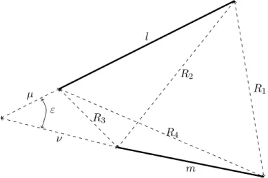
where L is the segment inductance in nanohenries and w and t come in centimetres. These units are explained in [89]. For the evaluation of the mutual inductances the for-mulas deducted by Groover [88] may be applied. For the case of two parallel segments as depicted in Fig. 3.6, the formula used to calculate mutual inductance is given by Eq. 3.23, wherelandmrepresent the segments lengths,dthe distance between them, andp andqrepresent the difference between the length of the segments.
l
d
r
m
q
Figure 3.6: Parallel segments.
2M = (Mm+r+Mm+q)−(Mr+Mq) (3.23)
Given that eachMi,j is calculated with the following formula,
![Figure 2.10: Excitation and eddy currents, and fields in a coil. I coil is the excitation current [2].](https://thumb-eu.123doks.com/thumbv2/123dok_br/16570308.737983/33.892.271.757.202.531/figure-excitation-eddy-currents-fields-coil-excitation-current.webp)
![Figure 2.11: Currents and fields in a coil printed on a lossy S i substrate [2].](https://thumb-eu.123doks.com/thumbv2/123dok_br/16570308.737983/34.892.132.710.157.499/figure-currents-and-fields-coil-printed-lossy-substrate.webp)