Miguel Ângelo Pereira Soares
Licenciatura em Engenharia de Micro e Nanotecnologias
Control System for Actuation and Sensing in Digital
Microfluidics Devices
Dissertação para obtenção do Grau de Mestre em: Engenharia de Micro e Nanotecnologias
Orientador: Rui Igreja, Professor Auxiliar, Faculdade de Ciências e Tecnologia,
Universidade Nova de Lisboa
Juri:
Presidente: Prof. Doutor Rodrigo Martins, FCT-UNL Arguente: Prof. Doutor Luís Gomes, FCT-UNL Vogal: Prof. Doutor Rui Igreja, FCT-UNL
i
Control System for Actuation and Sensing in Digital Microfluidics
Devices
Copyright © Miguel Ângelo Pereira Soares, Faculdade de Ciências e Tecnologia, Universidade Nova de Lisboa.
ii
iii
Acknowledgments
First of all, I’d like to thank my institution, the Faculty of Sciences and Technologies of the
University of Lisbon, for all the years it has sheltered me under its roof and for all the memories and people I will cherish for all my life. To my department, DCM, and the people who make it what it is, for the effort and dedication to lead me to where I am now. To CENIMAT, for having provided everything I needed for my work.
I’d like to thank my supervisor, Professor Rui Igreja, for his guidance and patience, and for the opportunity of integrating this incredible project.
To my work group and friends, Daniel Matos e Vasco Rodrigues, for their work and a very good mood even in the most stressing days.
To the rest of my friends, Gonçalo Rodrigues, Paul Grey and Ana Paula Correia, for their support and patience.
To my companion in love, Filipa Reizinho, for her presence and care, any time.
To my sisters, Paula Soares e Daniela Soares, for their help, even when they did not knew they were helping, or neither did I.
Control System for Actuation and Sensing in Digital Microfluidics Devices
v
Abstract
Digital Microfluidics (DMF) is a second generation technique, derived from the conventional microfluidics that instead of using continuous liquid fluxes, it uses only individual droplets driven by external electric signals.
In this thesis a new DMF control/sensing system for visualization, droplet control (movement, dispensing, merging and splitting) and real time impedance measurement have been developed. The software for the proposed system was implemented in MATLAB with a graphical user interface. An Arduino was used as control board and dedicated circuits for voltage switching and contacts were designed and implemented in printed circuit boards. A high resolution camera was integrated for visualization. In our new approach, the DMF chips are driven by a dual-tone signal where the sum of two independent ac signals (one for droplet operations and the other for impedance sensing) is applied to the electrodes, and afterwards independently evaluated by a lock-in amplifier. With this new approach we were able to choose the appropriated amplitudes and frequencies for the different proposes (actuation and sensing). The measurements made were used to evaluate the real time droplet impedance enabling the knowledge of its position and velocity. This new approach opens new possibilities for impedance sensing and feedback control in DMF devices.
Control System for Actuation and Sensing in Digital Microfluidics Devices
Control System for Actuation and Sensing in Digital Microfluidics Devices
vii
Resumo
Microfluídica Digital é uma técnica de segunda geração, que deriva da microfluídica convencional e em vez de utilizar fluxos de líquidos contínuos, utiliza apenas gotas individuais guiadas por sinais elétricos externos.
Nesta tese foi desenvolvido um novo sistema de controlo/medida para visualização, controlo da gota (mover, dispensar, juntar e separar) e medida de impedância em tempo real. O software para o sistema proposto foi implementado em MATLAB com uma interface gráfica de utilizador. Um Arduíno foi utilizado como placa de controlo. Foram desenhados e implementados circuitos dedicados à comutação de tensão e contactos para chips de Microfluidica Digital em placas de circuito impresso. Para a visualização uma camara de alta resolução foi integrada. Nesta nova abordagem, aos chips de Microfluídica Digital foi aplicado um sinal de dois tons, onde a soma de dois sinais AC independentes (um para as operações da gota e outro para a medida de impedância) foi aplicado aos elétrodos, e em seguida avaliados individualmente por um amplificador lock-in. Com esta nova abordagem, foi possível escolher as amplitudes e frequências apropriadas para os diferentes propósitos (atuação e medida). As medidas feitas foram usadas para avaliação da impedância da gota em tempo real, possibilitando o conhecimento da sua posição e da sua velocidade. Esta nova abordagem abre caminho para novas medidas de impedância e controlo por feedback nestes dispositivos.
Control System for Actuation and Sensing in Digital Microfluidics Devices
Control System for Actuation and Sensing in Digital Microfluidics Devices
ix
Table of Contents
ACKNOWLEDGMENTS ...III
ABSTRACT ... V
RESUMO... VII
TABLE OF CONTENTS ... IX
LIST OF TABLES ... XI
LIST OF FIGURES ... XIII
LIST OF ACRONYMS ... XV
LIST OF SYMBOLS ... XVII
MOTIVATION ... 1
1 INTRODUCTION ... 3
1.1 STATE OF THE ART ... 3
2 MATERIALS AND METHODS ... 9
2.1 DMF DEVICE CONTROL ... 9
2.1.1 Printed Circuit Board Design ... 9
2.1.2 Printed Circuit Board Manufacturing ... 9
2.1.3 Program Development ... 9
2.2 DMF DEVICE VISUALIZATION ... 10
2.2.1 Camera and DMF chip holder ... 10
2.3 DMF DEVICE MEASUREMENTS... 10
3 RESULTS AND DISCUSSION... 11
3.1 ASSEMBLING THE SYSTEM... 11
3.1.1 Control Board and PC serial communication ... 11
3.1.2 HVSU and Contact Board ... 11
3.1.3 3D printed DMF structure and acrylic support parts ... 11
3.1.4 Control Board and PC serial communication improving ... 12
3.2 TESTING THE SYSTEM ... 13
3.3 IMPEDANCE MEASUREMENT CIRCUIT ... 15
3.3.1 Static Measurements ... 16
3.3.2 Dynamic Measurements and the “dual-tone” system ... 20
3.3.3 Practical tests ... 22
Control System for Actuation and Sensing in Digital Microfluidics Devices
x
3.4 REAL-TIME POSITION AND VELOCITY DETERMINING ... 27
3.4.1 Calibration ... 28
3.4.2 Position and Velocity vs. Time ... 29
3.5 FEEDBACK SYSTEM ... 31
3.6 PRACTICAL APPLICATION ... 32
4 CONCLUSIONS ... 33
5 REFERENCES ... 35
APPENDIX ... 37
APPENDIX 1-SCHEMATICS AND LAYOUTS ... 37
Appendix 1.1: HVSU (High Voltage Switching Unit) ... 37
Appendix 1.2: Contacts Board ... 40
APPENDIX 2–LABORATORIAL PROCEDURES ... 42
Appendix 2.1: Printed Circuit Board Manufacturing... 42
APPENDIX 3–PROGRAM CODE ... 43
Appendix 3.1: Control Board (test with LEDs) ... 43
Appendix 3.2: Control Board (final) ... 46
Appendix 3.3: MATLAB GUI v. 1.0... 48
Appendix 3.4: MATLAB GUI v2.0 ... 51
APPENDIX 4–DMF SYSTEM STRUCTURAL SUPPORT ... 61
Appendix 4.1: 3D printed DMF support structure... 61
Control System for Actuation and Sensing in Digital Microfluidics Devices
xi
List of Tables
Table 3.1 – Characteristics of the DMF chip used to test the system... 14 Table 3.2 – Characteristics of the low-pass filter. ... 17 Table 3.3 – Electric characteristics of the different layers used at 1 kHz. ... 19 Table 3.4 – Adjusted values of parasitic impedance and double layer capacitance for 50, 70 and
Control System for Actuation and Sensing in Digital Microfluidics Devices
Control System for Actuation and Sensing in Digital Microfluidics Devices
xiii
List of Figures
Figure 1.1 - Effect of Electrowetting on Dielectric on a droplet, in a closed configuration and in
an open configuration, and its respective structure. ... 3
Figure 1.2 – Block diagram of the DMF chip control system. ... 4
Figure 1.3 - Schema of the impedance measurement system used by Ma et al. [21] and Sadeghi et al. [22]. Adapted from [21]. ... 5
Figure 1.4 - Schema of the measurement circuit used by Shih et al. [18]. Adapted from [18]. ... 6
Figure 1.5 - Feedback system presented by Shih et al. [20]. ... 6
Figure 3.1 – Chip support structure for DMF system. ... 12
Figure 3.2 – Hierarchic relation between the developed GUIs for the DMF control system. ... 13
Figure 3.3 – Layout of the chip used for all the tests. Chip composed by 6 electrodes and 2 reservoirs. ... 13
Figure 3.4 – DMF System Graphical User Interface version 2.0 Model 1. ... 14
Figure 3.5 – Droplet operations performed in the first test: moving a small droplet through electrodes (a-c) and dispensing a bigger droplet from the reservoir (d-f)... 15
Figure 3.6 – Schema of the measurement system assembled... 16
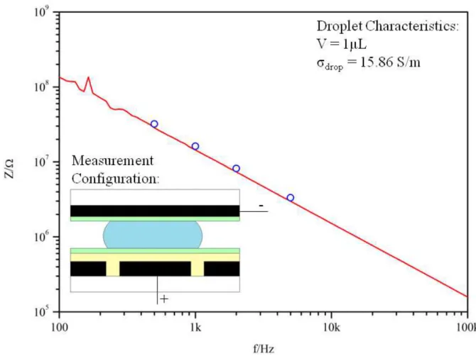
Figure 3.7 – Chip impedance modulus as a function of frequency (between 100 Hz and 1 MHz), using a droplet of salt solution (3M). In red, the measurements made with the Agilent 4294A and in blue, the data extracted from the proposed system, at 0.5, 1, 2, 5 and 10 kHz. ... 18
Figure 3.8 – Variability of relative impedance modulus with frequency for different conductivities in NaCl solutions. The conductivity of the solution of 3 M of NaCl was measured, 15.86 S/m... 19
Figure 3.9 – Comparison of relative impedance modulus of a low conductivity liquid (left; ultra-pure water, σ = 6.67x10⁻⁶S/m) and a high conductivity liquid (right; salt solution 3 M, σ = 15.86 S/m). ... 20
Figure 3.10 – Block diagram of the control system using a dual-tone signal... 21
Figure 3.11 - Chip impedance modulus as a function of frequency (between 100 Hz and 100 kHz), using a droplet of salt solution (3M). ... 22
Figure 3.12 –Impedance modulus measured by the “dual-tone” system upon droplet movement from one electrode to another, then back to the first one. Vmeas = 10 Vrms, fmeas = 1 kHz, Vmov = 70 Vrms, fmov = 10 kHz, Rfeed = 989 Ω. ... 23
Control System for Actuation and Sensing in Digital Microfluidics Devices
xiv
Figure 3.14 – Block diagram of the system used for the measurement of small impedance
variations in the DMF system. ... 25
Figure 3.15 – Schema of the aggregation of AuNPs in presence of salt solution... 25
Figure 3.16 – Variation of the impedance modulus measured with the AuNPs test. ... 26
Figure 3.17 – Schematic of the impedances measured by the DMF system. Simplified version on the right. ... 27
Figure 3.18 – Theoretical and experimental variation of the distance travelled over time, for 50, 70 and 90 V. ... 30
Figure 3.19 – Theoretical and experimental variation of the velocity over time, for 50, 70 and 90 V. ... 31
Figure 3.20 – Reaction of the horseradish peroxidase with H2O2. ... 32
Figure A.1 – Partial schematic of the High Voltage Switching Unit. The complete unit has four more AQW210SOP, as well as two resistors per switch. ... 38
Figure A.2 – Layout of the High Voltage Switching Unit. ... 39
Figure A.3 – High Voltage Switching Unit: Prototype. ... 39
Figure A. 4 – High Voltage Switching Unit: v2.0. ... 40
Figure A.5 – Schematic of the Contact Board. ... 40
Figure A.6 – Layout of the Contact Board. ... 41
Figure A.7 – Contact Board fastened to the DMF system structure... 41
Figure A.8 – Block diagram of the system assembled to test the code written for the Arduino (Control Board). ... 43
Figure A.9 – Results of the testing of the MATLAB program created. ... 43
Figure A.10 – Graphical User Interface of the communication bridge generated in MATLAB. ... 49
Figure A.11 – DMF System Graphical User Interface version 2.0 Menu. ... 51
Figure A.12 – DMF System Graphical User Interface version 2.0 Control Board Connection. ... 53
Figure A.13 – DMF System Graphical User Interface version 2.0 Image Analysis... 54
Figure A.14 – DMF System Graphical User Interface version 2.0 Model 1. ... 56
Figure A.15 – Support structure for the DMF system. ... 61
Control System for Actuation and Sensing in Digital Microfluidics Devices
xv
List of Acronyms
3D Three dimensional
ABTS 2,2'-azino-bis(3-ethylbenzothiazoline-6-sulphonic acid)
AC Alternate Current
AuNPs Gold Nanoparticles
CENIMAT Centro de Investigação em Materiais CMF Conventional Microfluidics
DC Direct Current
DCM Departamento de Ciências dos Materiais DMF Digital Microfluidics
EWD/EWOD Electrowetting on dielectrics GUI Graphical User Interface
GUIDE Graphical Unit Interface Development Environment
HD High Definition
HVSU High Voltage Switching Unit
ITO Indium Tin Oxide
LED Light Emitting Diode
MATLAB MATrix LABoratory OpAmp Operational Amplifier
PC Personal Computer
PCB Printed Circuit Board
PR Photoresist
RGB Red-Green-Blue
RMS Root Mean Square
Control System for Actuation and Sensing in Digital Microfluidics Devices
Control System for Actuation and Sensing in Digital Microfluidics Devices
xvii
List of Symbols
ε permittivity (F/m)
ρ resistivity (Ω.m)
σ conductivity (S/m)
A area (m2)
C capacity (F)
d thickness (m)
f frequency (Hz)
I current (A)
j imaginary number ( ) H2O2 hydrogen peroxide
NaCl sodium Chloride
R resistance (Ω)
Sn tin
V voltage (V)
Control System for Actuation and Sensing in Digital Microfluidics Devices
Control System for Actuation and Sensing in Digital Microfluidics Devices
Motivation
1
Motivation
Conventional microfluidics (CMF) emerged from the necessity of creating a platform for biosensors that used much less volume of reagents and performed biological tests much quickly. Digital microfluics (DMF), a descendant of the conventional microfluidics, is an area that is growing fast in the scientific world nowadays. Differently from its predecessor, DMF allows actuation over individual droplets, which lower even more the volume of reagents used, and enable the possibility of performing reactions at a much higher rate. This area of study presents itself as very interesting and refreshing in a society where faster things are expected (as microprocessors, for example).
The control system for actuation and sensing represents a crucial part in the whole DMF system that combines various fields of knowledge and resort to various tools, needed, for it to work. This means that there is a need to research for an efficient way of controlling the DMF chip, especially in the signals used for the actuation and monitoring the droplets movement.
Control System for Actuation and Sensing in Digital Microfluidics Devices
Control System for Actuation and Sensing in Digital Microfluidics
Devices
Introduction
3
1
Introduction
1.1
State of the Art
Conventional microfluidics is generally a system based in micro-channels enclosed in a monolithic substrate where liquids with a few microliters are mixed [1, 2]. This combination allows the application of this technique in various fields of knowledge as chemistry [3-5], biology [6-8], and medicine [9-12]. However, despite its diversity, it is limited in number of actions it is able to perform [2].
Digital microfluidics (DMF) is a descendant of this technique that instead of using enclosed micro-channels, it uses an array of electrodes to address individually liquid droplets by the application of electrostatic forces [13, 14]. The use of individual droplets causes a great reduce in the volume of samples required (it can be between picoliters and microliters), reaction rates are much higher and heat transfer is faster. These advantages opens the possibility of integration, to create lab-on-a-chip devices [14, 15].
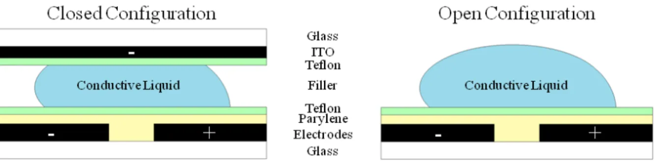
DMF relies on the electrowetting on dielectric (EWOD) effect to address the droplets, which means that when an voltage is applied across a dielectric layer, above which is a layer of a hydrophobic material, if an aqueous droplet is placed over this surface, (within the electric field created) its contact angle will be substantially reduced, i.e. wetting is verified (Figure 1.1).
Figure 1.1 - Effect of Electrowetting on Dielectric on a droplet, in a closed configuration and in an open configuration, and its respective structure.
Control System for Actuation and Sensing in Digital Microfluidics
Devices
Introduction
4
one is only composed by the plate described as the bottom plate for the closed format (Figure 1.1, right). Both of these formats are used depending on the application. The closed format is better suited for performing droplet operations, as for mixing, moving, splitting, and dispensing. However, in comparison, open format is better suited for integration of external detectors [16, 17]. Also, evaporation rate of droplets is much higher in the open format than the closed format, which can be relevant depending on the application [15].
Despite the chip configuration, digital microfluidics system is not only constituted by the chip itself. It is also needed a way to control the voltage applied to the electrodes, a way to visualize what is happening in the DMF chip (with a camera), and a measurement system to obtain information about the droplets (chemical reaction rates, position, velocity, impedance, etc.), which may vary from application to application. The control system is basically a bridge of communication between a computer or any user interface and a dedicated control board, which will drive a High Voltage Switching Unit (HVSU). Afterwards it receives a high voltage signal and, on command, can provide switching between the highest electric potential and the ground on each individual electrode (Figure 1.2) [13, 18-20].
Figure 1.2 – Block diagram of the DMF chip control system.
Control System for Actuation and Sensing in Digital Microfluidics
Devices
Introduction
5
electronic switches, from the dielectric and hydrophobic layers, etc.) it is sometimes difficult to extract that information.
To overcome that problem Fobel et al. [13] inserted a impedance-based sensor system in which a voltage divider was used with a 10 MΩ resistor in series with a reference resistor (it differs
according to the attenuation desired), to calculate the impedance, by evaluating the output voltage between both resistors . A similar system is used by Ma et al. [21] and Sadeghi et al. [22]: a resistor is used as a voltage divider, to acquire a voltage in a digital acquisition interface, and consequentially calculate the impedance (Figure 1.3).
Figure 1.3 - Schema of the impedance measurement system used by Ma et al. [21] and Sadeghi et al. [22]. Adapted from [21].
Control System for Actuation and Sensing in Digital Microfluidics
Devices
Introduction
6
Figure 1.4 - Schema of the measurement circuit used by Shih et al. [18]. Adapted from [18].
Later on, Shih et al. [20] present a new setup that consists, as well, in a voltage divider with two digital potentiometers controlled by an Arduino1 board. However it uses a buffer to avoid capacitive effects of the Arduino inputs in the feedback circuit (Figure 1.5).
Figure 1.5 - Feedback system presented by Shih et al. [20].
With these systems is possible to extract enough information to locate the droplet, know its velocity and its chemical status, and also reproduce a feedback system that is usually used to obtain a
Control System for Actuation and Sensing in Digital Microfluidics
Devices
Introduction
7
more homogenous movement of the droplet. Although, all of the setups share a common drawback: none of them are capable of separating the signal used for the droplet movement from the signal used for impedance measurement.
With this in mind, the final goal of this thesis is to develop a system capable of measuring the impedance in real time using a signal independently from the one used for the droplet movement. This
will be achieved by applying a “dual-tone” signal, where one frequency will be suited for the droplets movement and the other to extract information about the droplet electric properties, which are related to its physical and chemical properties. For that, firstly, it was required to assemble the whole control system to perform all the possible droplet operations.
Chronologically, there are three main goals. The first main goal is to design and implement a functional Digital Microfluidics system. That includes the design and production of the printed circuit boards for the High Voltage Switching Unit and Contact Board, the assembly of a support structure for the DMF system, programming the Control Board and the communication with the computer and the design of a Graphical User Interface, to control the DMF system.
The second main goal is to design and implement a system capable of converting the electric current flowing through the system into a voltage and using that voltage to calculate the impedance of the system and extract information about the droplet properties while microfluidics operations are being performed.
Control System for Actuation and Sensing in Digital Microfluidics Devices
Control System for Actuation and Sensing in Digital Microfluidics
Devices
Materials and Methods
9
2
Materials and Methods
To describe the methods applied in this thesis, the DMF system was divided in various parts: DMF device control, DMF device visualization and DMF device measurements.
2.1
DMF device control
In the DMF device control, the methods used relied in printed circuit board design, printed circuit board manufacturing, electrical components soldering and code writing. The system built was adapted from Dropbot open-source DMF system2.
2.1.1 Printed Circuit Board Design
For the board design of the High Voltage Switching Unit and the Control Board, software Cadsoft Eagle PCB Software version6.5.0 was used (freeware), where schematics and layouts were made. The schematics and the layouts produced are available in Appendix 1.
2.1.2 Printed Circuit Board Manufacturing
For the board manufacturing of the High Voltage Switching Unit, a double-sided copper-coated board with a coating of pre-sensitized photoresist was sensitized using a double-sided vacuum UV lamp unit, afterwards revealed and etched to create the HVSU board. Then 1mm holes copper for vias and contacts were drilled. Lastly the circuit board was immersed in a tin solution to deposit tin over the remaining copper. The procedure is described in Appendix 2.1: Printed Circuit Board Manufacturing. For the Control Board the same procedure was used, though the board was just one-sided. Components soldering was made using a soldering iron and tin solder (Sn60).
2.1.3 Program Development
The code to program the control board (Arduino MEGA 2560) was written in Arduino software while the code to control the control board was written in MATLAB3, using the GUIDE complemented with some hard code (Appendix 3 – Program Code).
2 http://microfluidics.utoronto.ca/trac/dropbot/wiki/ControlBoard
3 Multi-paradigm numerical computing environment and fourth-generation programming language.
Control System for Actuation and Sensing in Digital Microfluidics
Devices
Materials and Methods
10
2.2
DMF device visualization
The DMF device visualization consists in a HD Webcam (Microsoft LifeCam HD) and a DMF chip holder.
2.2.1 Camera and DMF chip holder
The holder was reproduced using a 3D printer, part by part, and then assembled. The 3D files used are available at the DropBot official website4. Two pieces of acrylic for the holder were designed in Adobe Illustrator and cut using a Universal Laser Systems VLS3.50. Images of the projected parts and the output are represented in Appendix 4 –DMF system structural support.
2.3
DMF device measurements
For the impedance measurements, an electronic circuit dedicated was designed and assembled. This circuit was basically a transimpedance amplifier that would result as an I/V converter. This transimpedance amplifier was constituted by a 1 kΩ feedback resistor (that could vary depending on the sensibility desired for the system), an AD549LH amplifier, and a 560 pF feedback capacitor.
Control System for Actuation and Sensing in Digital Microfluidics
Devices
Results and Discussion
11
3
Results and Discussion
3.1
Assembling the system
3.1.1 Control Board and PC serial communication
The first goal was to create a basic system that would allow the control of the HVSU. This means that the first part of the project to be prepared was the Control Board. A pre-code to test the functionality of the Control Board (Arduino) was written. This component decodes a binary word, sent by the user interface, which will be the PC, and sends a signal through its digital outputs that will control the HVSU. The preliminary test performed and its results are shown in Appendix 3.1: Control Board (test with LEDs).
After this test, a Graphical User Interface was designed and implemented in MATLAB to send the commands to the Control Board. This approach allows simplifying the Arduino code previously written for a more basic and, consequentially, faster response. The code written for the MATLAB GUI and the graphical interface created are available in Appendix 3.3: MATLAB GUI v. 1.0.
3.1.2 HVSU and Contact Board
The HVSU (High Voltage Switching Unit) is needed to control the switching between the high voltage and the ground as well as a Contact Board is needed to perform the necessary contacts with the DMF chip pads. Both boards where based on the open source DMF system DropBot5, but with some modifications. The boards’ schematics and layouts are available in Appendix 1.1: HVSU (High Voltage Switching Unit) and Appendix 1.2: Contacts Board, respectively. They were fabricated using the methods described in Appendix 2.1: Printed Circuit Board Manufacturing, where the HVSU was double sided and the contact board was one sided.
The Contact Board was designed to support up to 32 contacts. This means that the system supports up to four HVSUs (8 swithes per board).
3.1.3 3D printed DMF structure and acrylic support parts
Using as reference the DropBot open source material, the structure that would support the DMF device was printed on a 3D printer. A 3D computerized image of this structure is shown in Figure
Control System for Actuation and Sensing in Digital Microfluidics
Devices
Results and Discussion
12
A.15, Appendix 4.1: 3D printed DMF support structure, and a figure of the assembled chip support structure is shown in Figure 3.1.
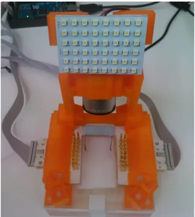
Figure 3.1 – Chip support structure for DMF system.
3.1.4 Control Board and PC serial communication improving
Control System for Actuation and Sensing in Digital Microfluidics
Devices
Results and Discussion
13
Figure 3.2 – Hierarchic relation between the developed GUIs for the DMF control system.
3.2
Testing the system
After the assemblage of the whole system, a test was performed. The test consisted in performing all the droplet operations with a droplet of a solution of NaCl (3M), using the available chips.
The configuration used was the closed format, represented in Figure 1.1, where the filler used was silicone oil. This configuration differs from the open format since a top plate and silicone oil were used. However, both have the same objective: to reduce the necessary applied voltage to the electrodes, in order to observe electrowetting and, consequentially, movement of the droplet. The chip layout is shown in Figure 3.3.
Control System for Actuation and Sensing in Digital Microfluidics
Devices
Results and Discussion
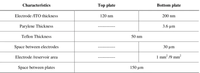
14 The DMF chip characteristics are presented in Table 3.1.
Table 3.1 – Characteristics of the DMF chip used to test the system.
Characteristics Top plate Bottom plate
Electrode /ITO thickness 120 nm 200 nm
Parylene Thickness --- 3.6 µm
Teflon Thickness 50 nm
Space between electrodes --- 30 µm
Electrode /reservoir area --- 1 mm2 /9 mm2
Space between plates 150 µm
For this particular layout a dedicated GUI was developed as represented in Figure 3.4. It has an image showing the layout of the selected model, and the buttons to select the desired state of each one of the electrodes. It also has the option to control manually or sequentially, using the table to store the states and the time on each state as on version 1.0. The Mirrored and Inverted checkboxes are to help the user to have an easier interaction with the DMF chip, if it is mirrored in both x and y axis, and if the camera mirrors the image (i.e. R1 from the camera image is R8 in the device).
Control System for Actuation and Sensing in Digital Microfluidics
Devices
Results and Discussion
15
A solution of 3 M of NaCl was used with some drops of red food coloring solution, so it was easier to see the droplet through the camera. The space of 150 µm between both plates was obtained using kapton tape. A droplet of 1 µL was placed in the reservoir and then the chip was closed and placed in the support structure. A voltage of 70 Vrms was applied to the reservoir and electrowetting was observed (the droplet wetted the reservoir), then the voltage was applied through the electrodes in order to dispense a smaller droplet from the reservoir, which is considered to be the most difficult droplet operation in DMF systems. This was achieved and the results are shown in Figure 3.5.
Figure 3.5 – Droplet operations performed in the first test: moving a small droplet through electrodes (a-c) and dispensing a bigger droplet from the reservoir (d-f).
The first droplet operations performed relied on moving the droplet by applying the high potential to the electrode where it is required the droplet to go, while connecting the present electrode to the ground. This is possible to see from a, through b, to c where the droplet is moving from one electrode to the next. The other droplet operation performed relied on dispensing a smaller droplet from the reservoir by stretching the droplet into various electrodes and shutting down the ones in the middle. This is possible to see from d, through e, to f, the droplet is stretched along 4 electrodes plus the reservoir, and split by applying a potential on the reservoir and the next electrode, and the two on
the other edge, leaving an electrode connected to the ground. The “H” on the image stands for High,
so that electrode is connected to high potential and the “L” stands for Low, which means it’s
connected to the ground. The ones without any identification are connected to the ground.
3.3
Impedance Measurement Circuit
Control System for Actuation and Sensing in Digital Microfluidics
Devices
Results and Discussion
16
different droplet electrical characteristics demands different frequency signals to extract relevant information from the droplet impedance.
3.3.1 Static Measurements
To measure the impedance it is necessary to know the current flowing through the chip. To be able to do so, a transimpedance amplifier was used to convert the current of the system in a voltage and connected to a lock-in amplifier. The schematic of the measurement system can be observed in Figure 3.6.
Figure 3.6 – Schema of the measurement system assembled.
Basically when a high voltage is applied to an electrode, an electrical circuit is closed, so the current generated will flow, through the layers of parylene, top Teflon and bottom Teflon, but also through the droplet. The amplifier, with the Rf in feedback, will perform a current-voltage conversion, transforming the current that flows from the whole system to Vout that is given by:
(Eq. 1)
Control System for Actuation and Sensing in Digital Microfluidics
Devices
Results and Discussion
17
Table 3.2 – Characteristics of the low-pass filter.
Rf Cf fc
989 Ω 560 pF 287 kHz
Afterwards, the signal will be received by the Lock-In that will lock to the frequency in its reference input, and evaluate the amplitude and phase of the signal in that frequency. Those values will be sent to the PC throughout the arduino. Once establishing the Rfeed value, the current that flows on the whole circuit, is given by:
(Eq. 2)
The impedance measured is related to all the impedances between the high voltage generator and the transimpedance amplifier. This means that the impedance measured is not only the droplet impedance but also the impedance from all DMF device layers and the parasitic impedances in the switching unit. The impedance modulus is given by:
(Eq. 3)
And so,
(Eq. 4)
Where Rf and Vin are constant, and Vout may only vary with the droplet impedance (assuming the chip impedance constant). That happens in two occasions: if some chemical reaction has taken place that changes the electrical properties of the droplet; or when the droplet is moving. In this last case, the measured impedance varies because the impedance between the two plates changes from oil impedance to the droplet impedance.
Control System for Actuation and Sensing in Digital Microfluidics
Devices
Results and Discussion
18
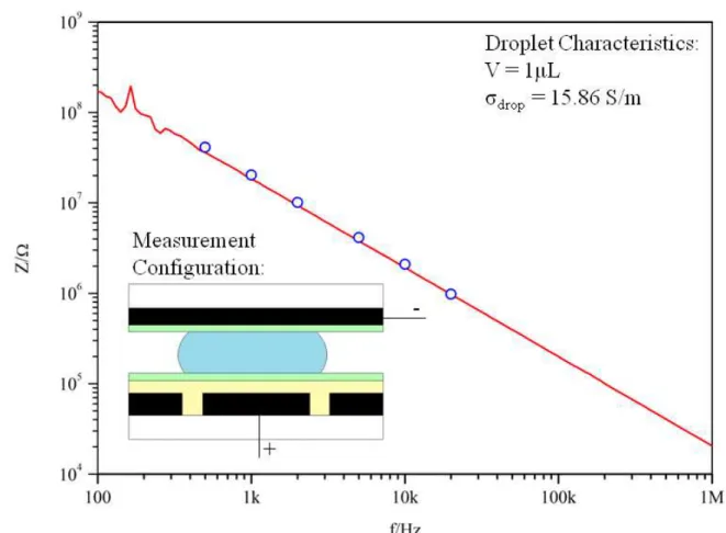
Figure 3.7 – Chip impedance modulus as a function of frequency (between 100 Hz and 1 MHz), using a droplet of salt solution (3M). In red, the measurements made with the Agilent 4294A and in blue, the data extracted from the proposed system, at 0.5, 1, 2, 5 and 10 kHz.
The measured impedances are related to the teflon and parylene capacitances and the droplet impedance. Knowing that the capacitance is given by:
(Eq. 5)
Where is the relative permittivity, the vacuum permittivity, the area of the electrodes and the distance between plates; and the resistance is given,
(Eq. 6)
Where, is the material resistivity (which is related to its conductivity by its inverse); and that the correspondent impedances are given by:
(Eq. 7)
Control System for Actuation and Sensing in Digital Microfluidics
Devices
Results and Discussion
19
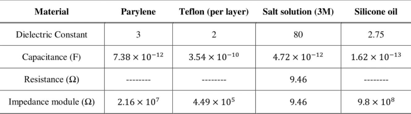
Then, also knowing the thickness of the layers of the chip, it is possible to determine the theoretical values of capacitance, resistance and impedance of those different layers. These values are presented in Table 3.3.
Table 3.3 – Electric characteristics of the different layers used at 1 kHz.
Material Parylene Teflon (per layer) Salt solution (3M) Silicone oil
Dielectric Constant 3 2 80 2.75
Capacitance (F)
Resistance (Ω) --- --- ---
Impedance module (Ω)
If the droplet is considered to be modeled by a capacitance in parallel with a resistance, its impedance is mainly resistive for lower frequencies and mainly capacitive for higher frequencies. In other words, if the impedance measured by this system at lower frequencies is much higher than the impedance of the droplet, any variation on the droplets impedance is not felt, for it is masked by the other layers impedance, but if this impedance is measured at higher frequencies, any variation on the droplets impedance is felt. However this characteristic changes with the conductivity of the droplet, as it can be seen on Figure 3.8.
Control System for Actuation and Sensing in Digital Microfluidics
Devices
Results and Discussion
20
3.3.2 Dynamic Measurements and the “dual-tone” system
Differently from the static measurements, the actual system it supposed to move the droplets while measuring its impedance. But, as seen before, there is a frequency above which the variations of impedance in the droplet are more visible, which means that it’s more appropriate for the impedance measurements. Nonetheless, while the measurement is better at higher frequencies, the movement may not be so. This is due to the fact that the droplet behaves like a dielectric above certain critical frequency, and below that frequency, the droplet behavior is manly conductive which is a condition for the electrowetting and consequently for droplet movement. This critical frequency, where ohmic and displacement currents are equal, is given by:
(Eq. 9)
Where and are the conductivity and dielectric constant of the droplet, respectively, and is the permittivity of the vacuum [23]. Assuming two extreme cases, where the conductivity of the liquid is very low (as ultra-pure water) or very high (as salt solution, for example 3M), the critical frequency becomes completely different, as observed in Figure 3.9.
Figure 3.9 – Comparison of relative impedance modulus of a low conductivity liquid (left; ultra-pure water, σ = 6.67x10⁻⁶ S/m) and a high conductivity liquid (right; salt solution 3 M, σ = 15.86 S/m).
Control System for Actuation and Sensing in Digital Microfluidics
Devices
Results and Discussion
21
measuring the impedance at frequencies over 1.5 kHz. The high conductivity liquid, on the other hand, allows a higher range of frequencies to actuate the droplet (up to 3.57 GHz) but for a better measure, frequencies above 3.57 GHz are required.
To be able to perform better measures and to still move the droplet by electrowetting, a dual-tone signal was implemented, using the sum of two independent AC signals. Because for the movement a high voltage is required, but not for the measurement, with this approach it is also possible to choose appropriate amplitudes (besides the frequency) for each interaction with the droplet (actuation or measurement). The new system is illustrated in Figure 3.10. Vmeas is summed with Vmov and connected to the reference of the Lock-in Amplifier, in order to evaluate only the remaining signal with the same frequency of that signal.
Figure 3.10 – Block diagram of the control system using a dual-tone signal.
Control System for Actuation and Sensing in Digital Microfluidics
Devices
Results and Discussion
22
Figure 3.11 - Chip impedance modulus as a function of frequency (between 100 Hz and 100 kHz), using a droplet of salt solution (3M).
As it is possible to observe the system proposed is capable of reliable impedance measurements and it is the first time that a system of this kind has been implemented in Digital Microfluidics.
3.3.3 Practical tests
Control System for Actuation and Sensing in Digital Microfluidics
Devices
Results and Discussion
23
Figure 3.12 – Impedance modulus measured by the “dual-tone” system upon droplet movement from one electrode to another, then back to the first one. Vmeas = 10 Vrms, fmeas = 1 kHz, Vmov = 70 Vrms, fmov = 10 kHz, Rfeed
= 989 Ω.
It is possible to observe that when the voltage is applied to the electrode where the droplet is, the measured impedance is around 14 MΩ. However, when the next electrode is turned on, the measured impedance triplicates and as the droplet starts to occupy the electrode where the voltage is being applied, the impedance decreases until it reaches the same value as before.
Control System for Actuation and Sensing in Digital Microfluidics
Devices
Results and Discussion
24
Figure 3.13 – Impedance modulus measured by the system upon droplet movement from one electrode to another, with different voltages (RMS).
As observed, the applied voltage is directly related to droplet velocity. Also observing Figure 3.13 it is possible to understand that the droplet impedance is related to its relative position in the electrode.
3.3.4 High Conductivity Droplets
Control System for Actuation and Sensing in Digital Microfluidics
Devices
Results and Discussion
25
Figure 3.14 – Block diagram of the system used for the measurement of small impedance variations in the DMF system.
To test this system a biochemical test was implemented. This test relied on the aggregation of gold nanoparticles that are dispersed in a solution. Gold nanoparticles, when dispersed in solution, tend to aggregate in the presence of a certain concentration of salt. The schematic of the reaction is represented in Figure 3.15.
Figure 3.15 – Schema of the aggregation of AuNPs in presence of salt solution.
There is a certain concentration of salt, for a concentration of AuNPs, above which the nanoparticles aggregate and below which the nanoparticles remain dispersed. To test this concentration some pre-tests were made. It was used a wide range of concentrations of salt: 10 mM, 25 mM, 50 mM, 75 mM, 90 mM, 100 mM, 1M, 2M and 3M. Solutions with 20 μL were placed in a respective eppendorf, previously prepared with 20 μL of AuNPs dispersed solution. The solutions
were mixed. The solutions of 1, 2 and 3 M instantaneously turned blue right after the solutions mixed. The solution of 100 mM took between 1 and 2 seconds before changing its color. The solution of 75 and 90 mM took about 3 minutes, while the solution of 50 mM took between 7 and 8 min before turning blue. The last two solutions, 25 mM and 10 mM didn’t turn blue, which means that the critical concentration is somewhere between 25 mM and 50 mM. A negative control test with phosphate tampon was used to verify the quality of the results. This control test didn’t change its color.
Control System for Actuation and Sensing in Digital Microfluidics
Devices
Results and Discussion
26
requires measuring the impedance and with a solution that takes as much as 7 min to fulfill its purpose it is possible to observe the changes in the impedance measured.
To perform the test, 1 μL of each solution was placed in its respective reservoir. The conditions
used in this test were the same as the previous tests. Smaller droplets were not dispensed in this test, rather the droplets were pulled to the center of the chip with a voltage of 70 Vrms to actuate. The signal to measure was turned off because of the limitations of the system available. Right after joining the droplets the signal was lowered to 10 Vrms with a frequency of 1 kHz. The feedback resistance was previously changed to 98.9 kΩz. The inverted signal was turned on at the same intensity and frequency as the other signal, and then balanced in order to obtain a value near zero in the lock-in amplifier. The value obtained was 2.33 Vrms. The variation of impedance measured is presented in Figure 3.16.
Figure 3.16 – Variation of the impedance modulus measured with the AuNPs test.
Control System for Actuation and Sensing in Digital Microfluidics
Devices
Results and Discussion
27
droplet along the whole electrode, including the metal tracks. Further work is consider to be necessary in order to take conclusions.
3.4
Real-time Position and Velocity Determining
The circuit assembled allows extracting the impedance of the system over time. This impedance has in account not only the impedance of the droplet but also the impedances of chip and parasitic impedances from the switches, between electrodes, cables, amplifier input, etc. Also, if the droplet is moving, the variation in the impedance measured is due to the parallel between the droplet and oil (filler).
The droplets used, however, are a salt solution of 3 M, i.e. an ionic solution. This means that with the application of an electric potential the ions in the droplet will rearrange themselves forming a double layer capacitance that will depend on the voltage applied. A schematic of the elements that influences the measured impedance is shown in Figure 3.17, left, and a simplified schematic is shown on the right.
Figure 3.17 – Schematic of the impedances measured by the DMF system. Simplified version on the right.
The impedances of the chip layers, the oil and the droplet, except for its double layer capacitance, are theoretically determinable as seen in Table 3.3. However, the parasitic and the double layer impedances are not.
Control System for Actuation and Sensing in Digital Microfluidics
Devices
Results and Discussion
28 3.4.1 Calibration
The calibration of the system consists in determining the undetermined impedances (double layer and parasitic). To do so, it is required to measure the impedance over time of the droplet moving
from an electrode to another while filming its position. With that it’s possible to crossover the movie with the measured impedance and extracting the experimental variation of the impedance with the distance traveled by the droplet.
The movement of the droplet, from an electrode to another, will make the impedance measured vary from a case where the droplet impedance is practically not measured to a case where the oil impedance is practically not measured. So, the capacitance of the oil and the capacitance of the droplet, respectively, will vary with the distance traveled according to:
(Eq. 10)
(Eq. 11)
Being l the size of the electrode and x the width of the electrode occupied with the droplet (distance traveled). The resistance of the droplet also varies with the distance traveled and it is given by:
(Eq. 12)
By Eq. 7 and Eq. 8 it is possible to calculate the respective impedances. The impedance of the droplet is the parallel of the impedances of Rdrop and Cdrop, in series with the double layer impedance.
The variation of the double layer capacitance (Eq. 13) will be similar to the droplet capacitance, varying from a maximum value, when it’s occupying the whole electrode, to null, when it’s not on the
electrode. The parasitic impedance (Eq. 14), however, will linearly vary from a maximum value, when the droplet isn’t on the electrode, to a minimum value, when the droplet has occupied the whole electrode. So, it is considered that the equations that would give the impedance of the double layer and parasitic capacitance, respectively, would be given by:
(Eq. 13)
Control System for Actuation and Sensing in Digital Microfluidics
Devices
Results and Discussion
29
Where x comes in millimeters. With these equations and Figure 3.17 in mind it is possible to find an equation for the theoretical impedance measured by the system as a function of the distance traveled, with only two unknown variables: CDL,max and Zparas,max. The general equation is given by:
(Eq. 15)
Plotting the experimental and theoretical values of impedance over distance traveled by the droplet, the values of CDL,max and Zparas,max were adjusted in order to obtain a better correlation between both curves, for different applied voltages (50 V, 70 V and 90 V). The curves for the measured impedance over time used for calibration are plotted in Figure 3.13. The optimum values adjusted for CDL,max and Zparas,max for each voltage are presented in Table 3.4.
Table 3.4 – Adjusted values of parasitic impedance and double layer capacitance for 50, 70 and 90 V.
Voltage CDL,max Zparas,max
50 V 4.7x10⁻¹² F
5x10⁷Ω
70 V 6.4x10⁻¹² F
90 V 7.2 x10⁻¹² F 5.1x10⁷Ω
3.4.2 Position and Velocity vs. Time
Control System for Actuation and Sensing in Digital Microfluidics
Devices
Results and Discussion
30
Figure 3.18 – Theoretical and experimental variation of the distance travelled over time, for 50, 70 and 90 V.
As it is visible, the theoretical and experimental curves, for each voltage, have a good correlation, what suggests that the model used is viable and that the system is capable of determining the position of the droplet over time. The distance travelled extracted from the film may input some minor errors in the convergence of the theoretical and experimental values. That is due to the fact that the distance travelled was measured in a representative number of frames of each videos, but the
droplet isn’t square, has considered, also, the metal of the electrodes mirrors the droplet which might
give an error in the droplet position. However, Figure 3.18 demonstrates that despite those minor errors, the model is relatively accurate.
Control System for Actuation and Sensing in Digital Microfluidics
Devices
Results and Discussion
31
Figure 3.19 – Theoretical and experimental variation of the velocity over time, for 50, 70 and 90 V.
Again, the values obtained suggest that the model is fairly accurate and opens the possibility of performing these calculations while measuring the impedance in real time, which will give information about the position and velocity of the droplet in real time.
3.5
Feedback System
Control System for Actuation and Sensing in Digital Microfluidics
Devices
Results and Discussion
32
3.6
Practical Application
As a practical application, an immune-assay was performed. After placing 1 µL of horseradish peroxidase (0.1 mg/mL) in phosphate buffer (pH 5, 100 mM), the enzyme, and 1 µL of the H2O2 in ABTS solution (0.05%), the substrate, in the reservoirs, a smaller droplet was dispensed from both the reservoirs, using a voltage of 90 Vrms for both.
The droplet with the substrate moves better than the droplet with the enzyme due to its higher conductivity, therefore easier to maneuver it the chip. After colliding both droplets, in the middle of the chip, the electrodes nearby were switched on and off in order to accelerate the mixing and the chemical reaction. The reaction occurred and the droplet became green (when previously both were transparent). The stages of the reaction are available in Figure 3.20. The change of color is due to having the ABTS in the solution, that will oxidize if the enzyme degrades H2O2 and the solution will turn green/blue. In a) two dispensed droplets are barely visible in the opposite sides of the chip, in b) the droplets have merged and a greenish coloration is starting to be visible and in c) the reaction was complete and the pretended coloration has been observed.
Control System for Actuation and Sensing in Digital Microfluidics Devices
Conclusions
33
4
Conclusions
In this thesis a control system for both actuation and sensing in Digital Microfluidic devices was developed.
The system for actuation was created using an Arduino as a control board and MATLAB graphical user interface as the interface to control Arduino. Boards for high voltage switching and for point contacts with the chip were designed and manufactured.
The system for sensing was created using a transimpedance amplifier and applying a “dual
-tone” signal. This signal was demodulated by the lock-in amplifier that allowed determining the system impedance and evaluating its changes during fluidic operations as for dispensing, moving, splitting and merging. This was the first time, in Digital Microfluidics, that a system of this kind was implemented and it was shown that the system performed reliable impedance measurements. The information extracted from the lock-in also allowed determining the droplet relative position and its velocity using a theoretical model that relates the position with the impedance measurements.
This system is functional and has been proven that it is capable of functioning as a biosensor, through the immune-assays performed. In future work, the gold nanoparticles agglomeration test may be a first step towards specific DNA detection.
As future improvements, it is important to lower the voltages used to drive the electrodes.
However, a master’s thesis that was elaborated in parallel with the present one, demonstrates the
capability of actuate a droplet with voltages as low as 10 Vrms, with a multi-layered dielectric layer device. Also, the feedback system was a great improvement to the DMF system, which would allow the system not to damage the devices used so quickly, and also being able to compensate some
imperfections on the device’s surface, with higher or lower voltage.
Control System for Actuation and Sensing in Digital Microfluidics Devices
Control System for Actuation and Sensing in Digital Microfluidics Devices
References
35
5
References
[1] M. J. Jebrail, M. S. Bartsch, and K. D. Patel, "Digital microfluidics: a versatile tool for applications in chemistry, biology and medicine," Lab on a Chip, vol. 12, pp. 2452-2463, 2012 2012.
[2] R. B. Fair, "Digital microfluidics: is a true lab-on-a-chip possible?," Microfluidics and Nanofluidics, vol. 3, pp. 245-281, Jun 2007.
[3] B. Davaji and C. H. Lee, "A paper-based calorimetric microfluidics platform for bio-chemical sensing," Biosensors & Bioelectronics, vol. 59, pp. 120-126, Sep 2014.
[4] Z. Olcer, E. Esen, T. Muhammad, A. Ersoy, S. Budak, and Y. Uludag, "Fast and sensitive detection of mycotoxins in wheat using microfluidics based Real-time Electrochemical Profiling," Biosensors & Bioelectronics, vol. 62, pp. 163-169, Dec 2014.
[5] E. Polshin, B. Verbruggen, D. Witters, B. Sels, D. De Vos, B. Nicolai, et al., "Integration of microfluidics and FT-IR microscopy for label-free study of enzyme kinetics," Sensors and Actuators B-Chemical, vol. 196, pp. 175-182, Jun 2014.
[6] B. W. Liu, D. Du, X. Hua, X. Y. Yu, and Y. H. Lin, "Paper-Based Electrochemical Biosensors: From Test Strips to Paper-Based Microfluidics," Electroanalysis, vol. 26, pp. 1214-1223, Jun 2014.
[7] S. R. Pullagurla, M. A. Witek, J. M. Jackson, M. A. M. Lindell, M. L. Hupert, I. V. Nesterova, et al., "Parallel Affinity-Based Isolation of Leukocyte Subsets Using Microfluidics: Application for Stroke Diagnosis," Analytical Chemistry, vol. 86, pp. 4058-4065, Apr 2014.
[8] B. Xiong, K. M. Ren, Y. W. Shu, Y. Chen, B. Shen, and H. K. Wu, "Recent Developments in Microfluidics for Cell Studies," Advanced Materials, vol. 26, pp. 5525-5532, Aug 2014.
[9] Z. Matharu, D. Patel, Y. D. Gao, A. Hague, Q. Zhou, and A. Revzin, "Detecting Transforming Growth Factor-beta Release from Liver Cells Using an Aptasensor Integrated with Microfluidics," Analytical Chemistry, vol. 86, pp. 8865-8872, Sep 2014.
[10] J. Jung, K. Kim, S. C. Choi, and J. Oh, "Microfluidics-assisted rapid generation of tubular cell-laden microgel inside glass capillaries," Biotechnology Letters, vol. 36, pp. 1549-1554, Jul 2014.
Control System for Actuation and Sensing in Digital Microfluidics Devices
References
36
[12] A. Benedetto, G. Accetta, Y. Fujita, and G. Charras, "Spatiotemporal control of gene expression using microfluidics," Lab on a Chip, vol. 14, pp. 1336-1347, 2014.
[13] R. Fobel, C. Fobel, and A. R. Wheeler, "DropBot: An open-source digital microfluidic control system with precise control of electrostatic driving force and instantaneous drop velocity measurement," Applied Physics Letters, vol. 102, May 13 2013.
[14] M. J. Jebrail and A. R. Wheeler, "Let's get digital: digitizing chemical biology with microfluidics," Current Opinion in Chemical Biology, vol. 14, pp. 574-581, Oct 2010.
[15] M. Abdelgawad and A. R. Wheeler, "The Digital Revolution: A New Paradigm for Microfluidics," Advanced Materials, vol. 21, pp. 920-925, Feb 23 2009.
[16] A. E. Kirby and A. R. Wheeler, "Digital Microfluidics: An Emerging Sample Preparation Platform for Mass Spectrometry," Analytical Chemistry, vol. 85, pp. 6178-6184, Jul 2 2013.
[17] T. Lederer, S. Clara, B. Jakoby, and W. Hilber, "Integration of impedance spectroscopy sensors in a digital microfluidic platform," Microsystem Technologies-Micro-and Nanosystems-Information Storage and Processing Systems, vol. 18, pp. 1163-1180, Aug 2012.
[18] S. C. C. Shih, R. Fobel, P. Kumar, and A. R. Wheeler, "A feedback control system for high-fidelity digital microfluidics," Lab on a Chip, vol. 11, pp. 535-540, 2011 2011.
[19] J. Gong and C.-J. Kim, "All-electronic droplet generation on-chip with real-time feedback control for EWOD digital microfluidics," Lab on a Chip, vol. 8, pp. 898-906, 2008 2008.
[20] S. C. C. Shih, H. Yang, M. J. Jebrail, R. Fobel, N. McIntosh, O. Y. Al-Dirbashi, et al., "Dried Blood Spot Analysis by Digital Microfluidics Coupled to Nanoelectrospray Ionization Mass Spectrometry," Analytical Chemistry, vol. 84, pp. 3731-3738, Apr 17 2012.
[21] X. Ma, S. Chen, C. Kim, and R. M. van Dam, "Towards On-Chip Chemical Reaction Monitoring by EWOD Impedance Measurement," presented at the MEMS 2014, San Francisco, CA, USA, 26-30 Jan. 2014.
[22] S. Sadeghi, H. Ding, G. J. Shah, S. Chen, P. Y. Keng, C.-J. C. J. Kim, et al., "On Chip Droplet Characterization: A Practical, High-Sensitivity Measurement of Droplet Impedance in Digital Microfluidics," Analytical Chemistry, vol. 84, pp. 1915-1923, Feb 21 2012.
Control System for Actuation and Sensing in Digital Microfluidics Devices
Appendix
37
Appendix
Appendix 1- Schematics and Layouts
Appendix 1.1: HVSU (High Voltage Switching Unit)
The purpose in the system of the High Voltage Switching Unit is to switch between a high electric potential and the ground, by receiving a digital signal from the Control Board. The switch has two photodiodes, both being fed by Arduino at 5 V in it positive terminal. The negative terminal in one is connected to the signal from the Control Board, while the other is connected to the inverted signal from the Control Board. When one of them is polarized the other is not (if one has a digital high signal, the other has a digital low signal), i.e. when one is polarized the output will be the high voltage, and when the other is polarized the output will be the ground.
Control System for Actuation and Sensing in Digital Microfluidics Devices
Appendix
38 Schematic:
Control System for Actuation and Sensing in Digital Microfluidics Devices
Appendix
39 Layout:
The drill marks are for better alignment before exposure of the board.
Figure A.2 – Layout of the High Voltage Switching Unit.
Board Produced:
Control System for Actuation and Sensing in Digital Microfluidics Devices
Appendix
40
Figure A. 4 – High Voltage Switching Unit: v2.0.
Electronic Material:
o 16x 309Ω 1206 resistor; o 8x 4.7kΩ 1206 resistor; o 1x 100nF 1206 capacitor; o 2x 1 row, 8 way connector; o 1x IC 74AC540;
o 8x AQW240S;
Appendix 1.2: Contacts Board
The purpose of the Contact Board in the system is to receive the high voltage from the HVSU and apply it to the DMF device through contact point probes. This board is constituted by 2 headers receiving the signals from the 4 HVSU and by the 32 contact point probes that will apply the same signals to the DMF device. The drill marks in the board are to fasten to the DMF system structure.
Schematic:
Control System for Actuation and Sensing in Digital Microfluidics Devices
Appendix
41 Layout:
Figure A.6 – Layout of the Contact Board.
Board Produced:
Figure A.7 – Contact Board fastened to the DMF system structure.
Electronic Material:
o 2x 2 rows, 2 way connectors;
Control System for Actuation and Sensing in Digital Microfluidics Devices
Appendix
42
Appendix 2
–
Laboratorial Procedures
Appendix 2.1: Printed Circuit Board Manufacturing
Firstly, a single or double layer board with copper and pre-sensitized photoresist and a protective cover above the photoresist is cut to meet the width and length of the layout design plus 2 centimeters. These extra centimeters have various purposes: to ensure that the layout is within the board and to ensure that all the layout is equally revealed. This is critical because in spite of having a protective cover, the edges of the photoresist becomes sensitized before the UV exposure which will compromise the revelation of the photoresist.
Then the layout is printed in an acetate sheet in duplicate (only the copper layers, i.e., top or bottom and pads, and for visual orientation vias, holes, and dimension. If it is a double layered board than the top and bottom layers in Eagle and printed but in separate sheets).
The duplicate sheets are aligned to create a better mask to sensitize the photoresist. If the board is double layered than the top and bottom prints are aligned as well.
The UV lamps are previously turned on for 3 minutes to heat up. Turn the heater of the revelation and the etching baths.
Removal of the protective covers of the board with haste, alignment of the acetate masks and the board and closure of the UV lamps exposure unit.
Power on the vacuum pump inside the expose unit (to avoid misalignments), and close the vacuum valve.
Exposure for 90 seconds.
Turn the vacuum pump of and open the valve (to air admission).
Open the exposure unit, avoiding the expose of daylight (or artificial white light), and quickly immerse the board in the revelation bath. Wait for a few seconds until the copper is visible. The layout of the circuit should be completely covered by photoresist.
Wash with water and immerse the board in the etching bath until the copper that was not covered by the photoresist is etched, being only visible the layout of the circuit.
Wash with water again and then with acetone to remove the photoresist.
Dry and immerse the board in a tin solution, to ease soldering and to avoid copper oxidation.
Control System for Actuation and Sensing in Digital Microfluidics Devices
Appendix
43
Appendix 3
–
Program Code
Appendix 3.1: Control Board (test with LEDs)
To understand the control of the High Voltage Switching Unit and how to program the Control Board so it could control the HVSU desirably, a testing code was made. This testing code relied in the existence of eight LEDs divided in two rows of 4 LEDs each. It uses the serial console of the Arduino software in order to give the directives to Arduino. The Arduino receives a series of commands including one for each LED, to light that LED specifically, a command to turn all the LEDs off, a command to know which LEDs are on and which are off, and a command to specify a state so the desired LEDs are lit or turned off. The layout of the test is shown in Figure A.8.
Figure A.8 – Block diagram of the system assembled to test the code written for the Arduino (Control Board).
After this pre-test, a MATLAB GUI was created to bridge the communication between the Control Board and the PC. This bridge was developed to be more user-friendly. The code for the MATLAB GUI, as well as the graphical interface associated, are available in Appendix 3.3: MATLAB GUI v. 1.0.
The results of the testing of the code are presented in Figure A.9: In a) a state where no “switch” is on, in b) a state where only the first “switches” of each line are on and in c) a state where all the
switches are on.
![Figure 1.3 - Schema of the impedance measurement system used by Ma et al. [21] and Sadeghi et al](https://thumb-eu.123doks.com/thumbv2/123dok_br/16694442.743764/25.892.213.682.405.676/figure-schema-impedance-measurement-used-ma-et-sadeghi.webp)
![Figure 1.4 - Schema of the measurement circuit used by Shih et al. [18]. Adapted from [18]](https://thumb-eu.123doks.com/thumbv2/123dok_br/16694442.743764/26.892.142.714.136.463/figure-schema-measurement-circuit-used-shih-et-adapted.webp)