Three Level Voltage Generation for Dual
Inverter Fed Open End Winding Induction
Motor drive.
G.SATHEESH†
Department of Electrical and Electronics Engineering, S.V.I.T., Anantapur, Andhra Pradesh., India‡
T. BRAMHANANDA REDDY
Department of Electrical and Electronics Engineering, G.P.R.E.C., Kurnool, Andhra Pradesh., India
CH. SAI BABU
Department of Electrical Engineering, J. N. T. U., Kakinada, Andhra Pradesh., India
Abstract:
An SVPWM scheme for a 3 level voltage generation is proposed in this paper. An open end winding induction motor, fed from a 3 level voltage realised by cascading 2 two level inverters. For the proposed drive configuration the DC link voltage required for 2 inverters is half of the DC link voltage used in the neutral point clamped inverter. The proposed configuration offers reduced circuit and control complexity. In this proposed scheme the lookup tables are not employed for the generation of the space vector locations and most time consuming task the sector identification is completely eliminated. The PWM signals are generated based on the instantaneous reference phase voltages only. The scheme ensures a smooth switching all through, ensuring equal switching duty for both the inverters.
Keywords: Open End Winding Induction Motor, Dual inverter, cascaded connection, V/f control, SVPWM.
1. Introduction
An Open end winding induction motor fed from both ends with 2 – Two level inverters results in output phase voltage structure, similar to a conventional 3 level NPC inverter configuration [3]. A number of techniques have been suggested to generate various configurations of 3 level inverters [1, 4 and 6]. In this paper A space vector based PWM switching scheme namely NSH switching proposed. The voltage stress and switching frequency is reduced for each inverter. In [6] one inverter is switched for six times in a given switching time and other inverter switched for 48 times. In the proposed scheme each inverter switches equally in a give switching time period. The total switching frequency is for each inverter is half of the switching frequency.
The most time consuming task sector identifications [4] and lookup tables’ employment is completely eliminated. The angle estimation and region determination are completely eliminated. Isolated DC power supplies are used in this scheme and the total amount of the DC voltage is half of the DC voltage used in [1]. The calculation part and the shifting of the sub hexagon centers [4] that is subtracting the required components along the a, b, c axes are not required.
By using the instantaneous reference voltages Va*, Vb*, Vc* the nearest sub hexagon centers and switching the inverters according to the selected sub hexagon centers is done here. In this paper, the modelling and simulations of cascading connection with separate DC sources have been preferred with Open End Winding Induction Motor load using the MATLAB and the results are discussed here.
2. Dual inverter fed open end winding induction motor
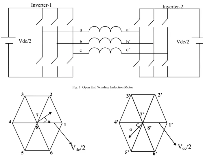
Fig. 1. Open End Winding Induction Motor
Fig. 2.a. Voltage Vector Locations for Inverter-1 Fig. 2.b.Voltage Vector Locations for Inverter 2
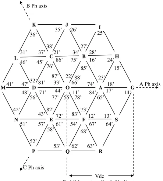
The Drive Configuration of figure 1 Consist of two 2-level inverters (Inverter -1 and Inverter -2), which feed the induction motor from both ends 2 isolated power supplies consisting of isolation transformers and rectifiers are required for the inverter system. The DC link voltage of each inverter is Vdc/2. The Space phasor combinations (23X23 = 26 = 64 Combinations as each inverter is assumed with 8 states independently of each other) from the 2 inverters is shown in fig.3.
In the figure 3 the |OA| represents the DC link voltage of individual inverters and is equal to the Vdc/2 while |OG| represents the DC link voltage of an equivalent single inverter drive and is equal to Vdc. It can be observed that the switching locations are similar to the conventional NPC inverter scheme, redundant switching combinations are available to realise a particular location. It can be also observed that the core hexagon ABCDEF with centerd O, can be plot by single inverter to obtain the other hexagons with centers A, B, C, D, E, F respectively can plot by using the other inverter. The hexagons namely OBHGSF, OCJIHA, ODLKJB, OENMLC, OFQPND and OASRQE are called as sub-hexagons. In the rest of paper the centers A, B, C, D, E, F are called as sub-hexagons centers (SHCs).
3. Proposed PWM scheme
The resultant space vector combination locations shown in figure 3 are obtained by superposing the space vector locations resulting from the inverter -2 at each space vector location caused by the inverter -1. Alternatively, the space vector locations of the resulting scheme may be obtained by superposing the centers of the left hexagon at each of the space vector locations of the right hexagon. The space vector combinations at the vertices and at the center of a given For example the space vector combinations at the vertices of sub hexagon OFSGHB (centered
1’
2’
3’
4’
5’
6’
V
dc/2
7’
α
8’
1
2
3
4
5
6
7
α
8
V
dc/2
a
b
c
a'
b’
c’
Inverter-1
Inverter-2
Fig. 3. Voltage vector positions for 3 level inverter
around the point ‘A’, Figure-3.), are obtained by clamping the inverter -1 to the state of 1(+ - -), while the inverter -2 switched in 1’, 2’, 3’, 4’, 5’ and 6’ respectively. The space vector combinations at the sub-hexagonal center ‘A’ are given by the active vector to which inverter-1 is clamped (in the current situation to state-1) and the null vectors of inverter -2 (states 8’ and 7’) respectively.
All the seven locations of a given sub hexagonal center (i.e six vertices and the corresponding sub hexagonal center) show redundancy of space vector combinations. For the sub hexagon OFSGHB, the space vector combinations for these seven locations may alternatively be obtained by clamping inverter -2 to state-4 (- + +) while the other inverter switches in all eight states.
3.1.Nearest Sub-Hexagon switching scheme
This scheme is based on the observation of that the space vector combinations at the vertices and the center of a given sub hexagon are obtained by clamping one inverter with an active state, while the other inverter switches in all eight states. The center of the nearest sub hexagon is obtained from the instantaneous reference voltage quantities which will be discussed here in further steps.
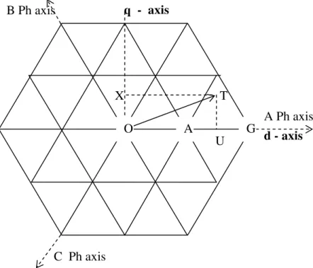
In the figure – 4, Vector OT represents the reference vector with its tip located in sector 7 ( in the triangle AHG). It is resolved in to two components OA and AT. The vector OA may be output of inverter -1which is clamped to state 1 (+ - -) through the sampling interval and the vector AT may be the output of other inverter -2,
Vdc
A Ph axis
C Ph axis
B Ph axis
O
A
B
C
D
E
F
G
H
I
J
K
L
M
N
P
Q
R
S
71’
11’
12’ 13’
14’
15’
16’
17’
18’
21’
22’
23’
24’
25’
26’
27’
28’
31’
32’
33’
34’
35’
36’
37’
38’
41’
42’
43’
44’
45’
46’
47’
48’
51’
52’
53’
54’
55’
56’
57’
58’
61’
62’ 63’
64’
65’
66’
67’
68’
72’
73’
74’
75’
76’
77’ 78’
81’
82’
83’
84’
85’
86’
Fig. 4. Resolving of switching vector of proposed scheme.
which is switched in all eight states. i.e the inverter -2 is switched with center A (the nearest sub hexagon center of OFSGHB). Otherwise the first vector OA is the output of the inverter 2 which is clamped to the state 1 (+ -) and the vector AT is the generated by switching the inverter -1. At each step of the interval the nearest sub hexagon center is identified by resolving the OT vector in to two components and first component is the output of the one inverter by clamped to an active state and other inverter is switched in all eight centers. In this scheme for the odd numbered centers inverter -1 is clamped i.e for A, C, E sub hexagon centers and the inverter -2 is switched, and for the other centers i.e B, D, F center sub hexagons inverter -1 is clamped and inverter -2 is switched. The roles of the individual inverters at each center is summarises in Table. 1.
Table. 1. Roles of Individual inverters at each NSH centers
NSHC A B C D E F
Inverter -1 Clamped to state-1 (+--) Switching mode Clamped to state-3 (-+-) Switching mode Clamped to state-5 (--+) Switching mode Inverter -2 Switching
mode Clamped to state-2 (++-) Switching mode Clamped to state-4 (-++) Switching mode Clamped to state-6 (+-+) The instantaneous phase reference voltage denoted by Vas, Vbs, Vcs corresponding to the reference voltage space vector OT are obtained by projecting the tip of OT onto the respective phase axes and multiplying them by a factor (2/3). The symbols Vds and Vqs denote the components of OT on the d and q axes, respectively. The reference voltages corresponding to the actual switching vector AT, denoted by Va, Vb and Vc, are obtained by the following procedure:
1. By using classical 3phase to 2 phase transformation method we can obtain the equivalent two-phase system references Vds and Vqs of the reference vector OT from the instantaneous phase reference voltages Vas, Vbs and Vcs.
−
=
Vcs
Vbs
Vas
Vqs
Vds
2
3
2
3
0
0
0
2
3
2. The Sub Hexagonal Center situated nearest to the tip of the reference vector OT is then determined. 3. The coordinates of the nearest Sub Hexagonal Center (NSHC) in the Vd – Vq plane (the point ‘A’ in
this example, Fig. 5), denoted by Vdnshc and Vqnshc are identified for all the six Sub Hexagonal Center s. For example, the coordinates of the point ‘A’ in the Vd –Vq plane are given by (Vdc/2, 0), similarly the coordinates of the point ‘D’ in the Vd –Vq plane are given by (-Vdc/2, 0)
A Ph axis
B Ph axis
C Ph axis
T
U
X
q - axis
d - axis
Fig. 5. Principle of Nearest Sub-Hexagon switching scheme
4. Since the vector OA is output by the clamping inverter, the coordinates of the switching vector (AT in the present case) denoted by Vdsw and Vqsw are given by
Vdsw = Vds – Vdnshc and
Vqsw = Vqs – Vqnshc
5. By using the classical two-phase to three-phase transformation, the modified reference phase voltages Vasw, Vbsw and Vcsw for the switching inverter are then obtained by transforming Vdsw, Vqsw into the corresponding three-phase variables
−
−
−
=
Vqsw
Vdsw
Vcsw
Vbsw
Vasw
3
1
3
1
3
1
3
1
0
3
2
6. If inverter-2 is employed as the clamping inverter, the modified references are used directly to generate the switching vector AT with inverter-1. On the other hand, if inverter-1 is used as the clamping inverter, it is obvious that the modified references must be negated to generate the switching vector AT with inverter-2.
7. It is important to note that the most important part of this algorithm is to find the nearest sub hexagonal center to the tip of the reference vector OT. The instantaneous reference voltages Vas, Vbs and Vcs normalised with respect to Vsr and their respective negations are shown in figure. 6.
From the figure.6, it may be noted that Vas is more positive quantity amongst these six quantities when 60o
≤ θ ≤ 120o and A is the nearest sub hexagonal center as recognised by figure 5. Similarly –Vas is the most positive amongst these six quantities when 240o ≤θ≤ 300o and D is the nearest sub hexagonal center. Thus it is clear that by finding the maximum value amongst these six quantities, one can determine the nearest sub hexagonal center.
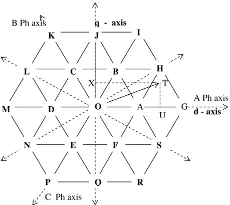
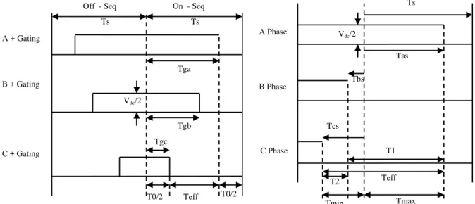
The basic switching algorithm described in [2] for the classical case of a two-level inverter feeding the conventional three-phase induction motor is extended for the dual-inverter system to compute the switching timings for individual inverters. This algorithm accomplishes the automatic generation of the gating pulses for the individual switching devices while placing the effective time exactly at the centre of a given sampling time period. The effective time is defined as the time for which the inverter supplies power to the motor in a given
A Ph axis
B Ph axis
C Ph axis
T
U
X
q - axis
d - axis
O
A
G
O
B
C
D
E
F
H
I
J
K
L
M
N
P
Q
R
sampling time period and is denoted by Teff . The sampling time period is denoted by Ts. The symbols Tga, Tgb and Tgc, respectively, denote the time duration for which a given motor phase is connected to the positive
Fig. 6. Recognition of the nearest sub hexagonal centers with instantaneous reference quantities.
rail of the input DC power supply of the inverter in the given sampling time period Ts. The timings Tga, Tgb and Tgc are termed as the phase switching times. The procedure to generate the gating pulses for the individual devices using this algorithm in sector-1 is pictorially depicted in figure 7 A similar procedure is adopted for all the other sectors.
Fig. 7. Switching Pulse Pattern of proposed PWM algorithm.
4. Simulation results
Fig.8: Pulses for the inverter -1 [Top Trace] and Inverter -2 [Bottom Trace].
Ts
Tas
Tbs
Tcs
Teff
Tmax Tmin
T1
T2 Vdc/2 A Phase
B Phase
C Phase Ts Ts
A + Gating
B + Gating
C + Gating
Vdc/2
Off - Seq On - Seq
Tga
Tgb
Tgc
Fig. 9 Pole voltages of individual inverters (Vao and Vao’) [Top Trace and Middle Trace] and Difference in pole voltages (Vaa’) [Bottom Trace]
Fig. 11 Pole Voltage (Vao) [Top Trace], Effective phase voltage (Van) [Middle Trace], Measured no-load current of the motor (Ia) [Bottom Trace] on no load.
Fig.13: Effective Motor Phase voltage (Van) with m=0.4.
Fig.14: Effective Motor Phase voltage (Van) with m=0.7.
Fig. 16: Normalized harmonic spectra for no load motor phase current of Proposed Algorithm
5. Conclusions
It is Clear that a conventional 3 - level voltage waveform can be synthesize by using the cascaded connection of the two 2 – level inverters.A space vector based PWM strategy for the dual inverter fed open-end winding induction motor, using only the instantaneous sampled reference voltages is presented in this paper. The proposed method does not involve any complex computations or mapping of sectors. The switching vectors for the dual inverter are automatically generated without using any look up table. The proposed method ensures equal switching’s in both the inverters without using any switching sequence table. Hence is simpler for implementation. The described PWM switching scheme is simulated using the MATLAB for the operation of
V/f controlled induction motor drive.
References
[1] Nabae, A., Takahashi, I., and Akagi, H.: ‘A neutral-point clamped PWM inverter’, IEEE- Trans. Ind. Appl., 1981, 17, (5), pp. 518– 523.
[2] Joohn-Sheok Kim and Seung-Ki Sul, “A novel voltage modulation technique of the space vector PWM”, in Conf. Rec. IPEC’95, Yokohama, Japan, 1995, pp. 742-747.
[3] Stemmler.H and Guggenbach.P. “Configuration of high power voltage source inverter drives”. EPE conf. Brighton, UK ’93, pp-7-12. [4] E.G. Shivakumar, K. Gopakumar, S.K. Sinha, Andre Pittet, V.T. Ranganathan, “Space Vector PWM Control of Dual Inverter Fed
Open-End Winding Induction Motor Drive”, EPE Journal, Vol. 12, No. 1, February 2002, pp. 9-18.
[5] K. Sivakumar, Anandarup Das, Rijil Ramchand, Chintan Patel and K. Gopakumar “A Three Level Voltage Space Vector Generation for Open End Winding IM Using Single Voltage Source Driven Dual Two-Level Inverter” TENCON ‘09
[6] V. T. Somasekhar and S. Srinivas, “Switching algorithms for a dual inverter fed open-end winding induction motor drive,” in Proc. IEEE IICPE, Mumbai, India, 2004.
[7] V.T.Somasekahr, K Gopa Kumar, Andre Pittet, V.T.Ranganathan “A Novel PWM Inverter switching strategy for a Dual Two-Level inverter fed open end winding induction motor drive.” IEEE Proc, 2001, pp.196-202.
[8] V.T Somasekhar, K.Gopakumar, " Three-level inverter configuration cascading two-level inverter" IEE Proc.Electr.Power Appl. Vo.1.50, No.3 may 2003,pp.245-254.
[9] Somasekhar, V.T., Gopakumar, K., Pittet, A., and Ranganathan, V.T.:‘PWM inverter switching strategy for a dual two-level inverter fed open end winding induction motor drive with a switched neutral’, IEE Proc., Electr. Power Appl., 2002, 149, (2), pp. 152–160. [10] Somasekhar, V.T., Baiju, M.R., and Gopakumar, K.: ‘Dual two level inverter scheme for an open end winding induction motor drive
with a single DC power supply and improved DC bus utilization’, IEE Proc., Electr. Power Appl., 2004, 151, (2), pp. 230–238. [11] Somasekhar, V.T., Baiju, M.R., and Gopakumar, K.: ‘Dual two level inverter scheme for an open end winding induction motor drive
![Fig. 9 Pole voltages of individual inverters (Vao and Vao’) [Top Trace and Middle Trace] and Difference in pole voltages (Vaa’) [Bottom Trace]](https://thumb-eu.123doks.com/thumbv2/123dok_br/18414022.360116/7.892.119.772.117.538/voltages-individual-inverters-trace-middle-trace-difference-voltages.webp)
![Fig. 11 Pole Voltage (Vao) [Top Trace], Effective phase voltage (Van) [Middle Trace], Measured no-load current of the motor (Ia) [Bottom Trace] on no load](https://thumb-eu.123doks.com/thumbv2/123dok_br/18414022.360116/8.892.129.762.114.413/voltage-trace-effective-voltage-middle-trace-measured-current.webp)


