doi:10.5194/jsss-5-433-2016
© Author(s) 2016. CC Attribution 3.0 License.
An 868 MHz 7.5 µW wake-up receiver with
−
60 dBm
sensitivity
Sadok Bdiri1, Faouzi Derbel1, and Olfa Kanoun2
1Faculty of Electrical Engineering and Information Technology, Leipzig University of Applied Sciences,
Wächter Str. 13, 04107 Leipzig, Germany
2Faculty of Electrical Engineering and Information Technology, Chemnitz University of Technology,
Reichenhainer Str. 70, 09126 Chemnitz, Germany
Correspondence to:Sadok Bdiri ([email protected])
Received: 7 September 2016 – Revised: 13 November 2016 – Accepted: 21 November 2016 – Published: 22 December 2016
Abstract. In wireless sensor networks (WSNs), batteries are unlikely to be replaced or recharged once they get
depleted, because of costs and feasibility. In a typical application, sensor nodes should be accessible and able to respond within a defined period of time, especially in real-time applications. However, the idle listening of the radio wastes most of the energy since the radio transceiver is constantly active. On the other hand, putting it into sleep state disconnects the node from the network. To cope with such a challenge, an ultra-low-power radio receiver referred to as a wake-up receiver (WuRx) handles the idle listening while keeping the main radio completely off. A WuRx consumes much less power than the main transceiver and triggers an interrupt only when a packet with a user-defined address is received. Embedding such a device enables better event-triggered applications where real-time behavior is required and a longer lifetime is mandatory. The proposed WuRx fea-tures practical sensitivity and includes the minimum number of active components in order to remain within the power budget. In this paper, an ultra-low-power WuRx with a power of 7.5 µW and a sensitivity of−60 dBm is developed. The decoding process of 16 bit of a wake-up packet (WuPt) takes less than 15 ms.
1 Introduction
The purpose of controlling one’s surroundings in the physi-cal world has become more relevant thanks to wireless sensor networks (WSNs). These networks include devices equipped with certain sensors in order to monitor the occurrence of ambient data and transmit them in an untethered manner. De-pending on the field of application, commonly, sensor nodes should be able to be deployed with major independency of wired power sources and using batteries instead. Presently, without energy saving techniques, a small battery with a large capacity together with the amount of demanded energy from a single node presents a real challenge when the lifetime of years is a requirement. Besides, to applications like haz-ardous work environments, nodes are unreachable once de-ployed; thus, maintenance becomes an even harder task. Fur-thermore, as a WSN incorporates a large number of nodes, which can go from tens to hundreds, the cost of a single node from production to maintenance should be as minimal
as possible. A sensor node mainly includes a processing unit, a radio chip, sensor(s), and a power source. The radio com-ponent spends most of the energy among the other parts. Re-searchers tend to reduce the power consumption by acting on the radio part. Commonly in WSNs, fewer data are transmit-ted in comparison to classical networks. Therefore, the radio can be principally turned off to save energy. On the other hand, this makes the sensor node unreachable and unable to respond to incoming packets from adjacent peers. Such an as-pect causes a trade-off between the power consumption and the radio chip activity.
Figure 1.Communication scheme in a duty-cycled radio.
applies to several scenarios. However, severe real-time pref-erences show that the overall system latency must be kept as short as possible, for which a very low duty-cycle radio scheme may be irrelevant. Conversely, an on-demand scheme is more likely to have very low communication latency with a reasonable energy consumption. Low-power radios known as wake-up receivers (WuRx) are intended to replace the main transceivers for idle listening tasks while consuming much less power. For extremely low latency communication, WuRx has to remain always on. If an ultra-low energy con-sumption can be realized, the sender network saves more en-ergy and can last longer than a network using a duty-cycle scheme. The main feature of the WuRx is to induce an inter-rupt mostly to a processing unit upon reception of a special radio frequency (RF) or wake-up packet (WuPt). Afterwards, the host node powers on the main transceiver to initiate the conventional network communication.
A WuRx, with a unique identifier, should incorporate a digital baseband (DBB) to identify WuPt and avoid false pos-itives. Commonly, WuRx designs adopt the ON/OFF keying (OOK) modulation technique due to its architectural sim-plicity. As WuRx consumes much less than conventional re-ceivers, performance parameters such as sensitivity are de-graded. State-of-the-art WuRxs work on improving the en-ergy consumption and sensitivity by either enhancing the re-ceiver architecture or choosing a more suitable technology. A passive radio receiver architecture was introduced by Gu and Stankovic (2004). The device uses the RF signal to raise a voltage level which will behave as an interrupt to the micro-controller (MCU). As an addressing technique, each WuRx receives a wake-up packet on a different frequency. Undoubt-edly, such a hardware design increases complexity for both a wake-up transmitter (WuTx) and WuRx. The WuRx has an interesting power consumption, but with a poor sensitivity. Improving the latter requires active elements. Nonetheless, more recent WuRxs manage to carefully realize it to end up with a balanced trade-off of energy/performance.
In this paper, we realize a low-power sensor node equipped with an ultra-low-power WuRx with at least−56 dBm sen-sitivity. The WuRx performs in sub-GHz bands, specifically 868 MHz. A discussion of recent WuRx designs is presented in Sect. 2. In Sect. 3, the proposed WuRx’s system design
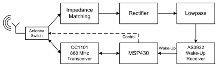
Impedance
Matching Rectifier Lowpass
AS3932 Wake-Up Receiver
MSP430
Wake-Up CC1101
8684MHz Transceiver Antenna
Switch Control
Figure 2.Proposed WuRx of Gamm et al. (2014).
is introduced. Hardware implementation details followed by the measurement results and a comparison with other designs are given in Sect. 4. Finally, conclusions and a summary of the results will be given in Sect. 5.
2 Design space
2.1 Architecture considerations
Realizing that the possibility of lowering the power con-sumption to an extreme low level is an idea which has been suggested by many contributors through the years. It starts by wondering how to detect an RF signal and how sensitive and power-hungry an RF detector can be. We can find sophisti-cated techniques which achieve excellent detection sensitiv-ity, but they dissipate more energy. As a commonly pursued strategy, the focus on designing wake-up radios using passive detection to guarantee the low-power budget is followed by attempts at enhancing sensitivity as well as other features.
Recent works (Pletcher et al., 2008; Marinkovic and Popovici, 2011) have focused on improving a single fea-ture at the cost of another, a trade-off of power consumption and sensitivity. In the real world, most applications require a practical balance of this trade-off in order to respond to the desired performance. Publications like Gamm et al. (2014) and Hambeck et al. (2011) considered coping with that chal-lenge. The efforts can be seen in the introduced WuRxs with
−53 and−71 dBm sensitivity levels and consuming 8.4 and 2.4 µW, respectively.
The WuRx as seen in Fig. 2 from Gamm et al. (2014) mainly down-converts the RF signal from 868 MHz to 125 kHz using zero bias Schottky diodes, which are config-ured as an AC–DC rectifier.
The incoming signal is OOK modulated where from the transmitter side, a digital bit “1” is encoded by transmit-ting the RF carrier, while a “0” is simply the absence of the carrier. The rectified signal is a square-wave waveform with a frequency equal to OOK signal bandwidth. The lat-ter is, then, fed to a low-frequency WuRx AS3932. The de-vice can correlate an up to 32 bit OOK modulated address with a sensitivity of 100 µVRMS, and it represents the main
(2016), a −55 dBm WuRx is introduced. It utilizes a com-parator to digitize the signal coming from the passive enve-lope detector to further feed it to a MCU. The offset voltage of the comparator sets the sensitivity of WuRx and dominates the entire WuRx energy consumption (1.2 µW) when MCU is in deep sleep. As soon as the MCU starts decoding, the en-ergy consumption increases to nearly 65 µW, which makes it highly susceptible to interferences and unwanted packets. A super-regenerative-based WuRx featuring a high sensitivity of −97 dBm is introduced in Petäjäjärvi et al. (2016). The WuRx has a power of 40 µW at a operational frequency of 28 MHz. As high-speed elements tend to consume more en-ergy, the consumption for this WuRx is only reasonable.
2.2 Technology considerations
WuRxs have been designed using either CMOS or off-the-shelf components. Concerning CMOS-based chips, publica-tions have introduced prototypes with practically higher sen-sitivity (Pletcher et al., 2008; Hambeck et al., 2011; Huang et al., 2014) than that of other architectures. In spite of draining a considerably high current, the overall power consumption remains low since they can operate at a very low voltage. In Pletcher et al. (2008) and Huang et al. (2014), the energy consumption is over 50 µW, which is still considered high for most event-triggered WSN applications. Passive enve-lope detectors based on nonlinear passive components such as Schottky diodes are often used to remain within the power budget. Standard CMOS features nonlinear characteristics and can be expressed by the exponential function of a diode’s currentIDin Eq. (1).
ID=IS
e
VD nVT
−1
, (1)
whereVD andIS are the diode’s forward voltage and
satu-ration current,nis the ideality factor, andVTis the thermal
voltage (Hambeck et al., 2011). At a small signal, which rep-resents the weak-inversion region of a MOS transistor, Schot-tky diodes and MOS transistors perform in a very similar manner when equally current biased. However, such detec-tors have poor sensitivity. Therefore, pamplification is re-quired to improve the radio sensitivity. Power-hungry com-ponents can accomplish such a task. It is challenging to im-plement them in a WuRx design.
A time-to-market factor has to be acknowledged when choosing a technology to design a WuRx. Particularly, de-signing CMOS integrated circuits (ICs) such as application-specific integrated circuits (ASICs) is pricey in terms of de-signing time and prototyping costs in spite of the potential performance. However, the benefit occurs when mass pro-duction is planned. Moreover, field programmable gate ar-rays (FPGAs) have the benefit of reducing production and non-recurring engineering (NRE). Some works incorporated FPGA chips mainly to perform as a DBB for address corre-lation with an energy consumption of a minimum of 5 µW
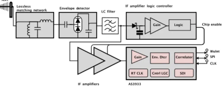
Figure 3.Wake-up receiver block diagram.
(Al-Uraiby et al., 2012; Pons et al., 2012; Jean-François et al., 2013; Rosello et al., 2011). The proposed WuRx uses off-the-shelf components with the purpose of accomplishing expeditious prototyping.
3 System design
Simplicity, sensitivity and energy consumption represent the main characteristics of an ultra-low-power WuRx. However, trade-offs exist between all the mentioned features; thus, finding an optimal point in between has been an interest-ing challenge. All along the designinterest-ing process of the WuRx, power consumption remained the number one issue to be controlled in every single step. Low-power active compo-nents are incorporated for the purpose of enhancing the sen-sitivity of the WuRx. In this section, the design analysis of all blocks of WuRx are discussed. The different parts of a WuRx circuit are illustrated in Fig. 3.
3.1 Envelope detector
The overall performance of WuRx severely depends on the envelope detector characteristics. For such a reason, compo-nents are carefully chosen in order to achieve the desired ob-jectives of the introduced design. The envelope detector de-tects the incoming signal by means of a passive receiver, no-tably using Schottky diodes HSMS-2852. The latter are zero biased and they provide fast switching. The diodes are opti-mized to be used with an input power of less than−20 dBm and below a frequency of 1.5 GHz (Avago Technologies, 2009).
The detector is configured as a Greinacher voltage doubler. Such a configuration provides higher output voltage. The ad-vantage of using such a configuration over a single diode is the voltage doubling at the output and also the increase in the signal-to-noise ratio (SNR).
10
-50 -40 -30 -20 -10 0 10 20
V
olt
ag
e
(V)
Input power (dBm) Voltage doubler
Single diode 1
10-1
10-2
10-3
10-4
Figure 4.Envelope output variation at two different configurations.
a square signal with a frequency equal to the ON/OFF fre-quency of an OOK signal.
3.2 Ripple filter
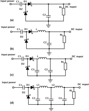
As the rectifier tends to convert a sinusoidal signal into a DC signal, the output voltage will have AC components referred to as ripples. The circuit is configured as a half-wave recti-fier. A distorted DC output has an impact on the overall per-formance of the complete circuit. Therefore, a ripple filter is added to fade out the undesired AC component.
With a shunt capacitor C2 connected to the rectifier
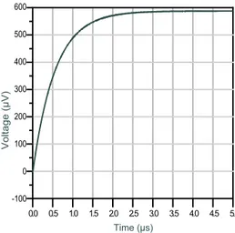
(Fig. 5a), the ripple voltage is decreased, thus having a smoothed output. However, at very low RF input power (<−50 dBm), the reduced ripple voltage still severely af-fects the output signal, which results in an alternating voltage instead of a constant DC output. Fig. 6 illustrates a simulation of rectified output voltage with an input power of−55 dBm at 868 MHz.
A decrease in RL will induce less output voltage with
larger ripples. Adding a series inductor Lforms an L-type LC filter (Fig. 5b). The reactance of the inductorXLopposes the AC components without reducing the DC output voltage. A capacitor filter is connected across the load resistanceRL.
The property of a capacitor is that it blocks the DC compo-nent and lets the AC compocompo-nent through. When the rectifier is fed with an AC signal, the capacitor charges rapidly to the peak voltage of the initial pulse. Depending on the value of RL, the capacitor will discharge until it is fed with the
sec-ond pulse. Thus, the ripple is shorted to the ground but DC appears at the output. Considering the reactanceXLandXC ofLandC, respectively, where
XC= 1
2ωC XL=2ωL ω=2πf, (2)
(a)
(c)
(d) (b)
Figure 5.RF–DC rectifier with(a)capacitor filter,(b)L-type LC filter,(c)π-type LC filter and(d)π-type and L-type LC filters.
0.5 1.0 1.5 2.0 2.5 3.0 3.5 4.0 4.5
0.0 5.0
0 100 200 300 400 500 600
-100 700
Time (µs)
V
olt
age
(µV
)
Figure 6.Output voltage of the rectifier with an L-type LC filter (Fig. 5b).
the ripple factorγ in terms ofXL andXC is calculated ac-cording to the following expression.
γL=
√
2XC 3XL =
√
2 12ω2LC
2
(3)
An increase inLandC narrows the ripple factor. Never-theless,Lhas to be large enough (>10 µH) to significantly reduce the ripple which will result in a big inductor size and manufacturing costs. Further improvement is made by adding another capacitorC3configured according to Fig. 5c.
factor expression is as follows:
γπ=
√
2 8ω3C
2LC3RL
. (4)
From Eqs. (3) and (4), a comparison between the perfor-mance of a π filter and an LC filter yields the expression (Eq. 5)
γπ= 3 2ωC3RL
γL. (5)
Consequently, the DC output has less ripple, with the advan-tage of an acceptable inductor value range. This configura-tion depends addiconfigura-tionally on RL andC3, which means the
lower theRLandC3, the higher theγ. A transient
simula-tion of the output voltage is shown in Fig. 7. Use of high-impedanceRL is acceptable since the circuit does not drive
high loads. Besides, by cascading stages of L-type LC filters (Fig. 5d), γ is much more reduced but requires additional components. In the introduced design, oneπ-type LC filter meets the required needs.
3.3 Intermediate-frequency amplifiers
Address decoder AS3933 (Austrian Mikro Systeme, 2010) has a sensitivity of a minimum of 80 µVRMS, which is
sim-ilar to that of AS3932. Concerning HSMS-2852, tangen-tial sensitivity TSS is −57 dBm for carrier frequency fc=
915 MHz and video bandwidth Bv=2 MHz (Avago
Tech-nologies, 2009). TSS stands for the lowest input signal power level higher than the minimum detectable signal, which cor-responds to an 8 dB SNR at the output (Avago Technologies, 2010). Several noise sources contribute to degrading TSS, most notably, thermal noise, shot noise and flicker noise. LoweringBvmainly reduces thermal noise, thus improving
TSS (SkyWorks Inc., 2008). Other efforts can be made to improve the noise quality. According to Gamm et al. (2014), the decoder is able to decode a signal with a minimum in-put power of −52 dBm. It can be seen that AS3932 limits the overall WuRx sensitivity as it is directly connected to the detector. An amplification needs to be performed in order to shift a small-signal voltage level coming from the detector above the minimum detectable voltage level of the AS3933.
Small-signal amplification within the micro-power budget faces several challenges. As a matter of fact, available com-mercial low-power amplifiers generally feature a high input offset voltageVOS, a low slew rate and a low gain–bandwidth
product (GBP). To raise an 18 kHz signal voltage level from µV to a detectable voltage, such amplifiers are not suitable for accomplishing the task. Instead, higher-performance de-vices are required. To preserve energy, amplifiers should function only during the WuPt decoding and remain shut down during channel monitoring of WuRx. In this work, the ON/OFF switching is controlled by a different block named an intermediate-frequency logic controller (IFLC). Now, the
0.5 1.0 1.5 2.0 2.5 3.0 3.5 4.0 4.5
0.0 5.0
0 100 200 300 400 500
-100 600
Time (µs)
V
olt
age
(µV
)
Figure 7.Output voltage of the rectifier with aπ-type LC filter (Fig. 5c).
nature of on-demand applications of WSNs and WuRx shows that, generally, nodes are in sleep state and power on only when the necessary communication takes place. Despite the amplifiers’ high power consumption, with such a communi-cation scheme, the resulting low duty-cycled amplifiers of-fer a very low overall energy consumption, which meets the power efficiency requirements. The overall power consump-tion of IF amplifiersPAmpis calculated in the following
ex-pression:
IAmp=DIAmp_Active+(1−D)IAmp_Sleep, (6)
wherePAmp_Activeis the power consumption of the amplifier
when active fortActiveandPAmp_Sleepwhen sleep/shutdown
fortSleep and the applied duty cycleD=t tActive
Active+tSleep. Now, according to the bandwidth expressed in Eq. (7) of an opera-tional amplifier, the higher the gain, the lower the bandwidth.
Bandwidth=Gain–bandwidth product
Closed loop gain (7)
The proposed design requires high precision and efficiency amplifiers with an optimal frequency / performance ratio. Other thanVOS, GBP,IAmp_Sleep, andIAmp_Active, other
pa-rameters should be taken into consideration to achieve the desired precision. Characteristics like input offset currentIOS
and input bias currentIBaffects directly theVOS, which
in-0 1e5 2e5 3e5 4e5 5e5 6e5 7e5 8e5 9e5 1e6
3 4 6 8
10−1 2 4 6 8
1
2 4 6 8
10
WuPts/Month
Curr
ent
(µA
)
Figure 8. Overall IF amplifier power consumption deviation
ac-cording to the number of received WuPts per month.
strumentation amplifier where GBP=250 kHz at a closed-loop gain of 20 dB, CMRR=120 dB,IAmp_Active=700 µA,
VOS=750 µV, and IAmp_Sleep=10 nA (Maxim Integrated,
2006). The MAX4461 has to last in active mode for a min-imum amount of time (tWuPt≤tActive) to fully amplify the
WuPt signal. Activating the amplifier is done through a SHDN pin.
The operation durations (tActiveandtSleep) of the IF
ampli-fier are controlled by a different circuit block. The WuPt lasts tWuPt=10.36 ms and the SHDN is guaranteed to be driven
fortActive=15 ms to meet the condition expressed earlier. To
simulate the overall power consumption of the IF amplifier, the number of the received packets increases and the duty cycle D is set for a total period of 1 month. According to Eq. (6), the total energy consumption changes proportionally and the variation is plotted in Fig. 8.
Once a wake-up packet (WuPt) is received, the IF ampli-fiers switch to active mode by means of an incoming signal at the SHDN pin. The signal is a low-to-high pulse which has to last slightly more than wake-up packet duration to avoid additional power loss. A current drain ofIAmp=0.13 µA for
a number of received packets of 104per month satisfies the required energy budget of the WuRx. However, 10e4packets per month is considered very high traffic based on the nature of on-demand or real-time applications.
3.4 Intermediate-frequency logic controller
The IF amplifier activates only when SHDN is driven HIGH by an IFLC. The idea is to generate a low-to-high pulse
us-1 2 3 4 5 6 7 8 9 10
0 11
100 200 300 400
0 500
Time (ms)
Voltage
(mV)
1 2 3 4 5 6 7 8 9 10
0 11
200 400 600
0 800
Time (ms)
Voltage
(mV)
1 2 3 4 5 6 7 8 9 10
0 11
0.0 0.5 1.0 1.5 2.0
-0.5 2.5
Time (ms)
Voltage
(V)
(a)
(b)
(c)
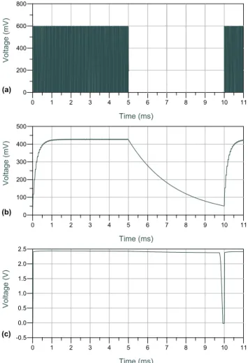
Figure 9.(a)18 kHz WuPt simulation (carrier burst);(b)peak de-tector waveform.(c)Final generated pulse by an IFLC.
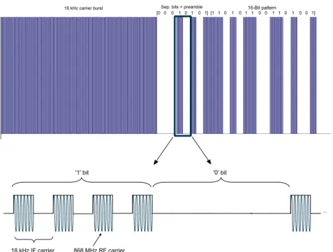
ing the received WuPt signal. The AS3933 decodes a spe-cific WuPt structure illustrated in Fig. 10. Unlike the data in WuPt, the carrier burst length is set to be unchanged. Ac-cordingly, the preamble and data pulses in WuPt are not taken into consideration to generate the wanted SHDN signal. The carrier burst laststC≃12tWuPt≃5 ms. The carrier burst has
... 18 kHz carrier burst Sep. bits + preamble 16-Bit pattern
[0I 0I 0I 1I 0I 1I 0I 1]I [1I 1I 0I 1I 0I 1I 1I 0I 0I 1I 1I 0I 1I 0I 0I 1]
868 MHz RF carrier 18 kHz IF carrier
'1'Ibit '0'Ibit
Figure 10.AS3933 wake-up packet structure.
SHDN implies that a HIGH signal should have an amplitude of minimum 0.7 VCC, and a LOW signal has to be maximum of 0.3 VCC. A comparator is incorporated to guarantee such logic control. The SHDN pulse is illustrated in Fig. 9c. The opAmp has a typical input voltage offset VOS= −100 µV,
which proportionally increases with the gain and consumes IOpAmp=330 nA. The comparator functions by comparing
the input signal voltage to a reference voltage, and then yields a digital signal indicating which is greater. In this design, a suitable reference voltage together with comparator hys-teresis are used to overcome false positives induced by ei-ther noise or DC offset. The chosen comparator TLV3691 consumes ICmp=75 nA with a maximum propagation
de-laytPD=45 µs (Texas Instruments, 2013). The overall power
consumption of the IFLC is calculated in the following ex-pression.
IIFCL=2IOpAmp+ICmp=735 nA (8)
3.5 Address decoder
AS3933 is a three-channel low-frequency WuRx which oper-ates within the 15–150 kHz frequency range. In the proposed design, the WuRx uses the ON/OFF low-power listening mode for energy economy. The mode functions by activat-ing all three channels simultaneously for a duration of 1 ms and deactivating them for a specific duration tAS3933_Sleep
which reaches a maximum value of 8 ms. The decoder is able to decode a 16/32 bit OOK modulated wake-up pat-tern. The WuPt structure should comply with the decoder’s as described by the manufacturer. The sequence contains a carrier burst, separation bits, a preamble, and a user-defined
pattern. The AS3933 supports Manchester-encoded packets. However, to avoid further complications in WuPt generation, Manchester encoding is disabled. On the other hand, the de-coder has a set of timing rules regarding carrier burst, pream-ble, and pattern durations and that depends on carrier and clock frequencies. For a carrier frequencyfc=18 kHz, the
two following relations are mainly used to determine the ex-act timings of the different parts of the WuPt in order to fulfill the AS3933 protocol rules.
fRCClk=fc
14
8 , (9)
92 fRCClk+
8 fc
< tC<
155 fRCClk
, (10)
wherefRCClkis the clock frequency. From Eqs. (9) and (10),
tC=4.9 ms is chosen in the current design and fRCClk=
31.5 kHz. Moreover, the decoder incorporates a specific pro-tocol with the purpose of recognizing preamble and pattern bits. A “1” bit for the decoder is a successive numberNC_T of ON/OFF periods of the carrier signal which has to last a user-defined numberNCLK_T of clock periods. The same principle applies for a “0” bit, but only with the complete absence of the carrier (OFF periods). The internal RC oscillator is used to generate the clock signal. The AS3933 supports a bit rate within the range of[1,8]kbit s−1. According to the design
peri-ods. The relation is calculated in the following expression.
NC_T = fc
fRCClk
NCLK_T (11)
A WuPt, which complies with the above settings, is illus-trated in Fig. 10, wherefc=18 kHz,NC_T =4 and the pat-tern is0xD669. The total WuPt duration istWuPt=10.3 ms.
With a 16 bit address length it is possible to have 256 unique patterns when Manchester encoding is disabled and 65 536 otherwise. AS3933 supports three modes of operation: stan-dard listening, scanning mode and ON/OFF mode. For the first, all channels are active simultaneously. For scanning mode, the listening is done on the channels one by one with the condition of having one active channel only at a time. The last mode scans all three channels at once for 1 ms, then switches them off to conserve energy for a configurable time toffranging from 1 to 8 ms. Fortoff=8 ms, the current
con-sumption of AS3933 is measured at 1.7 µA.
3.6 Wireless module
An open-source WSn platform referred to as PanStamp AVR (PanStamp, 2014) is used as a host for the designed WuRx. It features a low-power 8 bit 8 MHz MCU, the Atmega328P from Atmel (Atmel, 2016). Additionally, the PanStamp in-corporates the CC1101 radio chip (Texas Instruments, 2007), which operates at 433 and 868–915 MHz. The total power consumption of both chips in the lowest power-saving modes is PPan.S_Sleep=159 nA, which represents the main reason
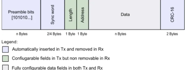
for choosing the wireless module. To wake up the mote, an interrupt has to be induced through a user-defined pin. The WuRx induces the corresponding interrupt once the correctly addressed WuPt is received. The PanStamp is also used as a wake-up transmitter (WuTx) since the radio chip is able to handle amplitude-shift keying (ASK) and OOK modula-tion schemes. With the chosen configuramodula-tion of the AS3933 in this design, the WuPt has a total length of 48 bytes. The CC1101 supports a 64 byte transmission FIFO queue, enough to handle the transmission of the complete WuPt.
Unlike Gamm et al. (2014), the number of bytes of a WuPt exceeds the FIFO size because of the higher carrier frequency (125 kHz) and the use of Manchester encoding. A solution they adopted is by re-filling the FIFO queue each time it is saturated until the WuPt is completely transmitted. Such a procedure elevates the complexity of the design. More-over, the CC1101 contains a specific packet structure pro-vided in Fig. 11. The packet is programmed in such a way that it matches the desired WuPt. Therefore, preamble, syn-chronization, length and address fields are set to the 0xAA
value to represent the carrier burst of WuPt. The data field contains the rest of the carrier burst, separation bits, pream-ble and pattern bytes. The code redundancy check (CRC) is disabled and its corresponding field contains0x0bytes. The
CC1101 is able to transmit a packet with transmission power up to+11 dBm.
Fully-configurable-data-fields-in-both-Tx-and-Rx Confiugarable-fields-in-Tx-but-non-removable-in-Rx Automatically-inserted-in-Tx-and-removed-in-Rx-Preamble-bits
S
y
n
c
-w
o
rd
L
e
n
g
th
A
d
d
re
s
s
Data
C
R
C
-1
6
Legend:
1-Byte 1-Byte 2/4-Bytes
n-Bytes n-Bytes 2-Bytes
[101010...]
Figure 11.CC1101 packet structure.
Figure 12.Assembled WuRx PCB and attached to a host node.
4 System evaluation
In this section, a proof of concept for the presented WuRx de-sign is carried out for experimental evaluation. Performance evaluation is expressed in terms of input impedance match-ing, power consumption, sensitivity, range communication and addressing capability. Different test beds are necessary to fill in a complete survey of measurements. A developed proof of concept can be seen in Fig. 12.
4.1 Hardware implementation
To concretize the explored design, prototypes are realized in order to gather multiple measurements. The circuitry is based on off-the-shelf commercially available components. The manufactured printed circuit board (PCB) is a two-layer 1.55 mm FR4 substrate with 35 µm copper width. The WuRx is interfaced with the host nodes through 24 pins. The WuTx node and the WuRx are programmed for the evaluation pur-pose. The execution flow chart is provided in Fig. 13.
Oscillator configura�on
IRQ handling
SPI interface configura�on
SPI interrupt handling
CC1101 ini�aliza�on
CC1101 interrupt handling CC1101 ASK/OOK
configura�on
AS3933 configura�on
AS3933 SPI interface
Deep sleep
Wake-up packet
data genera�on
Transmit wake-up packet Finish WuTx node Start Finish WuRx node
Figure 13.WuTx and WuRx node execution flow chart.
Table 1.PCB settings of PanStamp AVR and WuRx.
WuRx PanStamp AVR
PanStamp (2014)
Layers (mm) 2 4
Substrate FR4 FR4
Thickness (mm) 1.55 1
Width (mm) 22 17.7
Length (mm) 37 30.5
signals. To avoid problems caused by such aspects, PCB traces and transmission lines are carefully designed and kept as short as possible. The theoretical load impedance of the WuRx using the available diode model in advanced design system (ADS) from Agilent (Agilent Technologies, 2016) is Zload=33.6−j392. An impedance matching network is
essential to match the circuit to a 50system for maximum power transfer between source and load. Manufacturing con-ditions alter the impedance of diodes with every released product, thus deriving from a theoretical load impedance. For such reasons, practical Zload is measured by means of
a network analyzer to be able to determine the appropriate impedance matching network. However, the parasitic resis-tance of the Schottky diodes changes with the induced signal power, which alters theZloadof the circuit. A quasi-optimal
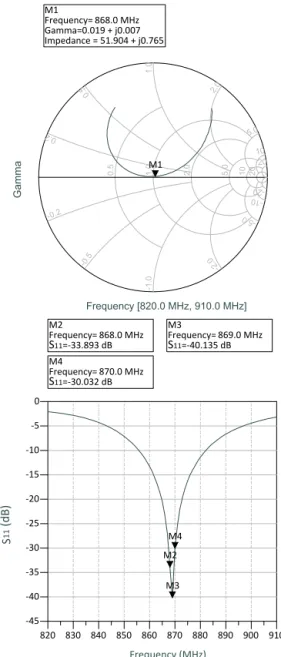
matching network is designed with respect to an input signal power of less than−40 dBm. Nonetheless, component trim-ming is also necessary to overcome the matching errors. A measurement of the reflection coefficient S11 at the WuRx
input on a log-magnitude plot and a Smith chart is provided in Fig. 14.
Changing the operation frequency of the WuRx within [867, 870] MHz does not alter the performance of the circuit, although a benefit is found as the frequency can be changed freely within a certain bandwidth. An example could be the
0. 5 1. 0 2. 0 5. 0 10 20 20 -20 10 -10 5.0 -5.0 2.0 -2. 0 1. 0 -1. 0 0. 5 -0. 5 0.2 -0.2
Frequency [820.0 MHz, 910.0 MHz]
G amma M1 M1 Frequency= Gamma=0.0192+2j0.007 Impedance2=251.9042+2j0.765 868.0 MHz
830 840 850 860 870 880 890 900
820 910 -40 -35 -30 -25 -20 -15 -10 -5 -45 0 Frequency2(MHz) S 1 1 2(dB ) M2 M4 M3 M2 Frequency= S11=-33.8932dB
868.0MHz
M4 Frequency= S11=-30.0322dB870.0 MHz
M3 Frequency= S11=-40.1352dB
869.0MHz
Figure 14.Measurement of the reflection coefficient (S11/ Ŵ) at the input of the WuRx.
use of one channel for WuRx and another channel for normal communication between nodes to avoid collision or interfer-ence.
To characterize the performance of the WuRx, a voltage output measurement of each block is performed individually during the WuPt decoding phase. A data capture from an os-cilloscope is shown in Fig. 15.
0 5 10 15 20 25 30 35 40 45 3
2 1 0 1 2 3 4 5 6
Volta
ge (mV)
0 5 10 15 20 25 30 35 40 45
0 0.02 0.04 0.06 0.08 0.1 0.12 0.14
Volta
ge (V)
0 5 10 15 20 25 30 35 40 45
0 0.5 1 1.5 2 2.5
Volta
ge (V)
0 5 10 15 20 25 30 35 40 45
0 0.5 1 1.5 2 2.5 3
Volta
ge (V)
Time (ms)
Ripple filter IFLC opAmps
AS3933 IFLC
Figure 15.Measurement of ripple filter, IFLC opAmps, IFLC and
AS3933 outputs while receiving a WuPt with an input power of −40 dBm.
However, a delay is noticeable between the first WuPt and the pulse, thus making the IF amplifiers amplify an incom-plete WuPt. The latter does not comply with the decoder’s WuPt protocol. The rise time of the opAmps output signal causes the delay. Moreover, the second WuPt is sent after 1.6 ms, which is shorter than the fall time of the opAmps and prevents the generated pulse from going LOW. Accordingly, the second WuPt is not compromised and fed to the AS3933 after amplification. Furthermore, as a practice, two WuPts are sent each time to compensate for the delay problem or by extending the carrier burst.
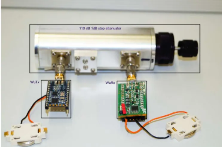
110 dB 1dB step attenuator
WuTx WuRx
Figure 16.Assembled WuRx PCB and attached to a host node.
0 15 30 45 60 75 95 105
2 4 6 8
10−2 2 4 6 8
10−1 2 4 6 8
1
2 4 6 8
10
Time (s)
Cu
rr
e
n
t
(m
A
)
Interrupted MCU (proper WuPt pattern)
WuRx (channel monitoring)
MCU: Sleep, WuRx: WuPt pattern mismatch
Figure 17. System current consumption in different operation
states.
4.2 Sensitivity
Table 2.Current consumption of WuRx and PanStamp in different states.
Components Channel monitoring WuPt decoding
(µA) (µA)
Envelope detector 0 0
Ripple filter 0 0
IFLC 0.73 0.735
IF amplifiers 0.03 2090
AS3933 1.7 8
PanStamp 0.159 0.159
Total 2.53 2099
104 2 3 4 5 6 7 8 9105 2 3 4 5 6 7 8 910 6
3 4 5 6 7 8 9 10
2 3
WuPt/Month
Cu
rr
e
n
t
(µ
A
)
Figure 18.Average WuRx current usage as a function of the
num-ber of received WuPts per month.
a transmission power ofPTx=3 dBm. Upon reception of a WuPt, the decoder interrupts the MCU, resulting in a blink-ing blue LED. A step further usblink-ing the attenuator, the trans-mission power is attenuated until no interrupt is induced to the MCU. A successful interrupt can be seen till an attenu-ation level of 63 dB. Now, a spectrum analyzer is connected to the attenuator instead of the WuRx. At 868.01 MHz, the measured signal amplitude varies within[−60.5,−60]dBm, with the same attenuation level. Therefore, the WuRx’s min-imum sensitivity is considered to bePS= −60 dBm.
4.3 Power consumption
Energy usage characterizes a WuRx design. With that in mind, an energy usage profile analysis is performed on a host node with an embedded WuRx. The measurement covers possible system operational modes. As illustrated in Fig. 17, the measurements last 110 s. At first, the WuTx is
config-Table 3.Range test at different WuTx transmission powers.
Transmission power Distance
(dBm) (m)
−10 8.3
0 26.2
3 40.2
10 82.5
11 92.9
Table 4.Wake-up receiver specifications summary.
Specification Value Condition
Sensitivity −60 dBm 4.57 kbit s−1, PER=1 % 10.3 ms latency Input impedance 33.6−j392 Simulated Wake-up pattern 16 bit No Manchester Bit rate 1–8 kbit s−1 Decoder bit rate Supply voltage 2.85–3.6 V
Current supply 2.53 µA Channel monitoring 2099 µA WuPt decoding Power-on time 10 ms
ured to continuously send two WuPts every 0.5 ms. The pat-tern included in the WuPts matches the one configured in the WuRx’s decoder. By starting the measurement, the receiving node is set to deep sleep mode, while the WuRx monitors the channel for an incoming WuPt. On average, the system con-sumes 2.5 µA of current. After an elapsed time of∼35 s, the WuTx starts transmitting WuPts, making the WuRx success-fully interrupt the MCU. The consumption jumps to 4 mA; the MCU remains active for certain time while performing tasks, and then switches back to deep sleep mode. After a to-tal duration of 70 s, the WuTx is programmed to send WuPts with patterns different than that of the WuRx. After initiat-ing the WuPts transmissions, the WuRx consumes 2.1 mA, which is mostly caused by the IF amplifier stages.
Furthermore, Table 2 summarizes the current consumption of WuRx parts for different operation modes including the host node. The WuPt power consumption is crucial when de-coding a WuPt.
Application of a WuRx implies that a WuPt is sent only at event-triggering trends. For such reasons, the total duration in which the WuRx decodes a WuPt is significantly less than the duration of channel monitoring. For evaluation purposes, the WuRx’s activity time is set attActive=35 ms. The average
current consumptionIWuRxis calculated in Eq. (12).
IWuRx=ICM+D(ID−ICM), (12)
whereICM andID are the current consumptions of WuRx
Table 5.Wake-up receiver prototype comparison.
This work Hambeck et Marinkovic and Gamm et Pletcher et
al. (2011) Popovici (2011) al. (2014) al. (2008)
Frequency (GHz) 0.868 0.868 0.433 0.868 2
Current (µA) 2.5 2.4 0.270 2.78 104
Sensitivity (dBm) −60 −71 −51 −53 −72
Range (m) 82b 304c 10d 37b N/A
Data rate (kbps) 4.5 20/200 5.5 NA 100
Addressing X X X X
Implementation OtSa 130 nm OtSa OtSa 90 nm
aOff-the-shelf.b10 dBm Tx power.c6.5 dBm Tx power.d0 dBm Tx power.
Eq. (13).
D=NPt/M
tactive
ttotal
(13)
The resulting relation is plotted in Fig. 18.
For 104received WuPts packets in 1 month, the average current consumption isIWuRx=2.76 µA.
4.4 Range
Improving a radio receiver’s sensitivity is mainly performed to extend the wireless coverage of the network. Nevertheless, other parameters like antenna gains and path losses also have an impact on the communication distance R. The relations between these parameters are expressed in the Friis equation (Eq. 14).
Pr
Pt =
GrGt
λ
4π R
2
, (14)
wherePrandPtare, respectively, the received and
transmit-ted signal power.GrandGtrepresent the antenna gains of the
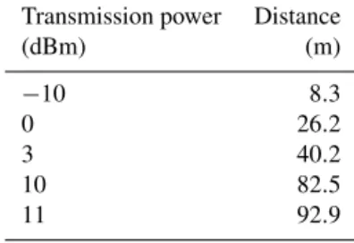
receiver and the transmitter, respectively. However, such a re-lation stands in an ideal condition where reflections, diffrac-tions and atmospheric absorption are not present. Therefore, the communication range is significantly different between indoor and outdoor applications. A practical range test of the network is realized in a free-space line-of-sight glance to measure the maximum possible coverage. The WuTx is set fixed on a pole at a height of 1.5 m and the WuRx is re-allocated until no WuPt is received. The used antennas are omnidirectional monopole antennas with a gain of 2 dBi. De-pending on the WuTx transmission power, different obtained ranges are listed in Table 3.
With a sensitivity of −60 dBm, the resulting range be-tween the WuRx and the WuTx is considered the widest coverage achieved by a WuRx implemented with
off-the-shelf components whilst regarding the energy consumption. At 10 dBm, a received WuPt is observed at a maximum dis-tance of 82 m. As expected, this is lower than the equiva-lent distance of 137.7 m, calculated from Eq. (14). Neverthe-less, these results are still better than Gamm et al. (2014), Marinkovic and Popovici (2011), and Magno et al. (2016). Characteristic WuRx parameters are summarized in Table 4. The present WuRx features are compared to those of re-cently published ultra-low-power radios and are provided in Table 5.
5 Conclusion
Ultra-low power for real-time constrained wireless WSNs is introduced. The paper describes the rationale behind the sys-tem design and the protocol details of a wake-up receiver. A novel WuRx architecture is adopted by taking the benefit from the communication scheme of an event-triggering ap-plication. Such architecture makes it possible to enhance the WuRx sensitivity while remaining within the micro-power budget. The current design is able to achieve a sensitivity of
−60 dBm while consuming 2.53 µA of a current in channel monitoring mode and is able to decode a 16 bit wake-up pat-tern. At 10 dBm of WuPt transmission power, a communica-tion range of nearly 82 m in the line-of-sight scheme is ob-served. Such coverage enables most of the on-demand WSNs applications. The WuRx performance is affected by the inter-ferences. Further revisions aim to resolve this issue as well as incorporate an MCU and transceiver on the same board.
6 Data availability
Sadok Bdiri received the engineering diploma in com-puter and embedded systems from the National Engineering School of Sousse (ENISo), Sousse, Tunisia, in 2011, an MS degree in robotics from the National Engineering School of Sfax (ENIS), Sfax, Tunisia, in 2013, and is currently pursu-ing a PhD degree in information technology and electrical engineering at the Leipzig University of Applied Sciences, Germany. In addition to wake-up receivers, he is also con-cerned with low-power radios and embedded systems.
Faouzi Derbelhas been Professor for Smart Diagnostic and Online Monitoring at the Leipzig University of Applied Sci-ences, Germany, since 2013. His research activities are fo-cused on wireless sensor networks and sensor systems with intelligent signal processing. In 2001, he obtained his PhD degree in electrical engineering from the University of the Bundeswehr Munich. From 2000 to 2012 he held different positions within Siemens and Qundis Advanced Measuring Solutions, e.g., systems engineer, head of the product inno-vation department and head of research and development. In 2012, he was Professor for Electrical Measurement Tech-nologies at the University of Applied Sciences Zwickau, Ger-many. Faouzi Derbel is a member of many technical groups dealing with short-range devices. He is Editor-in-Chief of the ASSD (Advances in Systems, Signals and Devices, Issues on Communication and Signal Processing, De Gruyter Verlag, Germany) and holds many awards and patents.
Olfa Kanoun has been a university professor of measure-ment and sensor technology at Chemnitz University of Tech-nology, Germany, since 2007. Her research focus is on the design of sensors and sensor systems. For more than 15 years, she has worked on power-aware wireless sensors with a focus on energy harvesting and energy management. Other research interests are in nanocomposite sensors and impedance spectroscopy.
Acknowledgements. This work has been supported by the
Autarkic Intelligent Sensor Network For Production (AIS) project within sub-project Energy-efficient and reliable wireless sensor communication (EMT). The project is funded by the European Science Foundation (ESF).
Edited by: R. Morello
Reviewed by: two anonymous referees
References
Agilent Technologies: Advanced Design System 2016.01, Datasheet, available at: http://literature.cdn.keysight.com/litweb/ pdf/5988-3326EN.pdf?id=921864, last access: 15 June 2016. Al-Uraiby, A., Yoshigoe, K., Seker, R., Babiceanu, R., and
Yil-mazer, N.: FPGA Implementation of Low-profile Wake-Up Ra-dio Receiver for Wireless Sensor Networks, in: The 1st IEEE Global Conference on Consumer Electronics 2012, 2–5 October 2012, Tokyo Japan, 2012.
Atmel: Atmel 8-Bit Microcontroller, datasheet,
available at: http://www.atmel.com/Images/
Atmel-42735-8-bit-AVR-Microcontroller-ATmega328-328P_ Datasheet.pdf, last access: 1 Decmeber 2016.
Austrian Mikro Systeme: 110–150 kHz AS3932 3D Low Fre-quency Wakeup Receiver, datasheet, revised 2015, available at: http://ams.com/chi/content/download/23636/413647/ (last ac-cess: 1 August 2016), 2009.
Austrian Mikro Systeme: 15–150 kHz AS3932 3D Low Frequency Wakeup Receiver, datasheet, revised 2015, available at: http: //ams.com/eng/Wake-up-receiver/AS3933 (last access: 2 Febru-ary 2016), 2010.
Avago Technologies: HSMS285x-Series, datasheet, available at: http://www.avagotech.com/docs/AV02-1377EN (last access: 5 January 2016), 2009.
avagotech.com/docs/5091-0169E (last access: 5 August 2016), 2010.
Bdiri, S.: Envelope_Detector_ADS, doi:10.17632/6d44wht7n3.1, 2016.
Gamm, G. U., Stoecklin, S., and Reindl, L. M.: Wake-Up Re-ceiver Operating at 433 MHz, in: 2014 IEEE 11th International Multi-Conference on Systems, Signals & Devices (SSD14), 11– 14 February 2014, Castelldefels-Barcelona, Spain, 2014. Gu, L. and Stankovic, J. A.: Radio-triggered wake-up capability for
sensor networks, in: Real-Time and Embedded Technology and Applications Symposium, 2004, Proceedings, RTAS May 2004. 10th IEEE, 25–28 May 2004, Toronto, Canada, 27–36, 2004. Hambeck, C., Mahlknecht, S., and Herndl, T.: A 2.4 µW Wake-up
Receiver for Wireless Sensor Nodes with−71 dBm Sensitivity, in: International Symposium on Circuits and Systems (ISCAS 2011), 15–19 May 2011, Rio de Janeiro, Brazil, 534–537, 2011. Huang, X., Harpe, P., Dolmans, G., de Groot, H., and Long, J. R.: A 780–950 MHz, 64 µW Power-Scalable Synchronized-Switching OOK Receiver for Wireless Event-Driven Applications, IEEE J. Solid-St. Circ., 49, 1135–1147, 2014.
Jean-François, P., Jean-Jules, B., and Yvon, S.: Modeling, design and implementation of a low-power FPGA based asynchronous wake-up receiver for wireless applications, Analog Integr. Circ. S., 77, 169–182, 2013.
Magno, M., Jelicic, V., Srbinovski, B., Bilas, V., Popovici, E. M., and Benini, L.: Design, Implementation, and Performance Eval-uation of a Flexible Low-Latency Nanowatt Wake-Up Radio Re-ceiver, IEEE T. Ind. Inform., 12, 633–644, 2016.
Marinkovic, S. J. and Popovici, E. M.: Nano-Power Wireless Wake-Up Receiver With Serial Peripheral Interface, IEEE J. Sel. Area. Comm., 29, 1641–1647, 2011.
Maxim Integrated: MAX4461 Precision Instrumentation Ampli-fier, datasheet, available at: https://datasheets.maximintegrated. com/en/ds/MAX4460-MAX4462.pdf (last access: 8 July 2016), 2006.
PanStamp: Panstamp-Avr, 868–915 MHz low power Wireless Mod-ule, datasheet, revised 2015, available at: https://github.com/ panStamp/panstamp/wiki/panStampAVR.-Technicaldetails (last access: 14 November 2015), 2014.
Petäjäjärvi, J., Mikhaylov, K., Vuohtoniemi, R., Karvonen, H., and Iinatti, J.: On the Human Body Communications: Wake-up Re-ceiver Design and Channel Characterization, EURASIP J. Wirel. Comm., 2016, 1–17, 2016.
Pletcher, N., Gambini, S., and Rabaey, J. M.: A 2 GHz 52 µW Wake-Up Receiver with−72 dBm Sensitivity Using Uncertain-IF Ar-chitecture, in: IEEE International Solid-State Circuits Confer-ence, ISSCC 2008, San Francisco, CA, USA, 3–7 February 2008, Digest of Technical Papers, 524–525, 2008.
Pons, J.-F., Brault, J.-J., and Savaria, Y.: An FPGA Compatible Asynchronous Wake-Up Receiver for Wireless Sensor Networks, in: 10th IEEE International NEWCAS Conference, 17–20 June 2012, Montreal, Quebec, Canada, 2012.
Rosello, V., Portilla, J., and Riesgo, T.: Ultra low power FPGA-based architecture for Wake-up Radio in Wireless Sensor Net-works, in: IECON 2011 – 37th Annual Conference of the IEEE Industrial Electronics Society, 7–10 November 2011, Melbourne, Victoria, Australia, 2011.
SkyWorks Inc.: Mixer and Detector Diodes, available at: http: //www.skyworksinc.com/uploads/documents/200826A.pdf (last access: 2 July 2016), 2008.
Texas Instruments: CC1101, Low-Power Sub-1 GHz RF
Transceiver, Datasheet, revised 2013, available at: http://www.ti.com/lit/ds/symlink/cc1101.pdf (last access: 9 July 2015), 2007.