Equalization in Hard Disk Drive Read Channels
Nuno Miguel de Figueiredo Garrido
Instituto Universitário de Lisboa (ISCTE-IUL)Instituto de Telecomunicações (IT-IUL) Lisboa, Portugal
nuno.garrido@iscte.pt
Francisco António Bucho Cercas
Instituto Universitário de Lisboa (ISCTE-IUL)Instituto de Telecomunicações (IT-IUL) Lisboa, Portugal
Francisco.cercas@iscte.pt Abstract—This paper presents a comprehensive
non-exhaustive comparative study of hard disk drive read-channel equalization techniques used in the readback process of magnetically stored information. The main read channel architectures: partial-response maximum likelihood (PRML) and decision feedback equalization (DFE) based systems, are compared in power consumption, layout area, data signalling rate and data density. This work focuses on the key component of the read channel, presenting a continuous-time analog solution for the pulse-slimming equalizer capable of reducing power consumption and die area by a factor of ten, whilst showing equivalent response to a FIR filter implementation.
Keywords—Peak-detection (PD); PRML; DFE; MDFE I. INTRODUCTION
Hard disk drives (HDD) store data by magnetizing a thin ferromagnetic film coating on an endurable physical foothold. The first solutions in magnetic hard disk drive storage for personal computers were based on conventional peak-detection read channels relying on the zero crossings of the differentiated input signal, to sample the input at its local minimum or maximum value. Later more elaborate designs include equalizer blocks with high frequency boost for pulse-slimming. The equalizing target of the system is strongly dependent on the physical properties of the playback and write processes, and hence, on the magnetic head response. Conventional inductive C-shaped or metal in gap (MIG) read heads, in which the flux flows parallel to the film coating on the disk surface, gave way to magnetoresistance (MR) and giant magnetoresistance (GMR) and in turn to tunnelling magnetoresistance (TMR). With perpendicular magnetic recording (PMR), the orientation of the flux on the veneer changed from parallel to perpendicular to the film coating thus allowing even tighter magnetic packing of up to 1Tbit per square inch of areal density. These advances together with cost and power efficiency have kept hard disk drives as the primary massive information storage choice, ten times cheaper than SSD especially for high capacity devices.
The properties of the communication channel, including read head characteristics can be treated as reasonably linear and time invariant. Therefore, a proper linear time-invariant system can be used to model the physical medium of the channel. The step response of the read back procedure is easy to extract based upon measured data from a single flux transition. The relative movement of the stored magnets on the disk’s surface
in respect to the read head causes a variation of the magnetic flux that flows through the head core. The changes in the direction of magnetization represent encoded binary data bits, thus the variation in time of the magnetic flux density flow through an electric circuit wire loop coiled on the read head generates an electric field, as results from Faraday’s law expressed in its integral form by
dt d t
v()=− φ. (1)
The most widely used step response model to a positive transition in magnetic flux polarity, is the Lorentzian model given by 2 50 2 1 1 ) ( ⎟⎟ ⎠ ⎞ ⎜⎜ ⎝ ⎛ ⋅ + = pw t t s (2)
In this model constant pw50 denotes the pulse width at 50% of its peak value. The corresponding pulse is depicted in figure 1, along with other common pulse shapes often used in signal processing, such as sinc, Gaussian and modified Lorentzian, all normalized to the peak value. In this model, t=0 corresponds to the instant that the read head hoverflies the boundary region of two adjacent magnets of opposite polarities. Most read channel architectures use clock recovery schemes to sample the input at this instant.
Figure 1. Read head pulse model
The portion of the response obtained for negative instants (precursor) reflects the physical fact that the influence of flux transition is sensed by the read head before it actually reaches the transition boundary, thus, since this effect precedes the optimum sampling instant, it effectively corresponds to a prior awareness of a future event, and therefore is inherently non-causal. Likewise, the postcursor response designates the
-0,25 0 0,25 0,5 0,75 1 -2 -1,5 -1 -0,5 0 0,5 1 1,5 2 Mod. Lorentzian Lorentzian Sinc Gaussian pw50
part of the pulse that follows the transition instant. The superimposition of two consecutive flux transitions denoting consecutive ones, usually designated as dipulse or dibit response, represents the effect of allowing Inter Symbolic Interference (ISI) to occur between adjacent bits, and is frequently used to characterize the response of the read channel.
User bit density (UBD) is defined as the pw50/T ratio, where T denotes time (or distance) between consecutive bits. As data density increases, the flux reversals are packed more tightly interfere and significant overlapping occurs, leading to inter-symbolic interference and to data bit errors, timing errors, peak shifts, peak drops. All of these can contribute significantly for the reduction of bit error rates (BER). To reduce interference whilst augmenting bit-density, the magnetic fields must decrease, thus peak detection becomes a week solution, especially at user bit densities pw50/T superior to 1. Several coding procedures and data constrains have been used in magnetic read channels as a result of this effort, and the read channel topology greatly depends on the chosen coding strategy as will be shown in section II. In sections III and IV we present a realization of a Multilevel Decision Feedback Equalization (MDFE) system with a continuous-time analog allpass filter for the pulse-slimming equalizer, and show it is capable of reducing power consumption and die area based on transistor level simulation, whilst showing equivalent response to a long finite impulse response (FIR) filter implementation. Section V concludes the paper.
II. READ CHANNEL ARCHITECTURES
Peak detection has been the main market solution for read channels for several decades, combining the lowest implementation cost with high efficiency. In 1990 IBM introduced its first-generation partial-response maximum likelihood (PRML) read channel technology in hard disk-drives.
A. Partial response maximum likelihood read channels
The PRML approach [1-5] differs from peak detector read channels, which do not compensate for ISI, by using advanced high-speed digital filtering to shape the read signal frequency and timing characteristics to a desired partial response (PR), and by using maximum-likelihood sequence detection (MLSD) to determine the most likely sequence of data bits that was written to the disk. Different classes of partial response read channels share the same simplified structure depicted in figure 2.
Figure 2. Partial response read channel block diagram
The basic architecture includes fast analog to digital converter (ADC) and a PR coding digital FIR adaptive equalizer to cancel ISI, usually followed by a simplified Viterbi algorithm detector. Different approaches to the coding are available all based on the partial response polynomial given by
. (3)
This delay polynomial derives from the z-transform of the equalizer function where D = z -1. The differentiating function
of the read head on the NRZ pattern is usually given by (1-D) thus most PR schemes use m=1. Partial response coding based on m=1 and n=1, denominated Class IV (PR4), is a simple and elegant realization of PR, where each voltage pulse results in two samples, thus delaying the decision in time, as given by PR polynomial 2 1 ) 1 ( ) 1 ( ) (D D D D P = − ⋅ + = − . (4)
An improved solution designated as extended partial response Class IV (EPR4) using m=1 and n=2 prolongs the response in time, given that each isolated pulse results in a sequence of three voltage samples (1,2,1) as a consequence of the quadratic form of term (1+D)2. Further development of PR class IV designated as E2PRML or E2PR4 using m=1 and n=3
can increase in linear density and disk capacity, without increasing BER, but at the expense of more complex signal-processing and power consumption [6-7]. Power consumption in digital blocks is roughly proportional to the signal frequency leaving short margin for data rate increases, and hence strongly limiting their application in HDD read channels, although still showing to be robust solutions for optical data systems such as DVD/Blu-ray [8-9]. Table 1 summarizes the results for data rate, power consumption, and die area of relevant PRML read channel solutions.
Table 1. PRML channel evolution
Year Technology Data Rate Power Area
1994 0.8µm CMOS [1] 72 Mb/s 1.50 W – 1995 0.5µm BiCMOS [2] 16 MB/s 1.20 W 26 mm2 1996 0.6µm CMOS [3] 130 Mb/s 1.35 W 28 mm2 1996 0.7µm BiCMOS [4] 150 Mb/s 1.55 W 47 mm2 1996 0.5µm BiCMOS [5] 200 Mb/s 0.85 W 20 mm2 1996 1.0µm CMOS [6] 160 MHz 0.46 W 23 mm2 1999 0.35µm CMOS [7] 300 MHz 0.23 W 0.8 mm2 2001 0.18µm CMOS [8] 150 Mb/s 0.18 W 1 mm2 2006 0.35µm CMOS [9] 300 MHz – 12.8 mm2 High-speed acquisition and sharpening of the magnetic-head data input-pulses, is done mainly at the expense of high silicon area (thus high cost) and high power consumption especially on high frequency channels. These limitations have led to the study of alternative solutions with equivalent equalization target but based on decision feedback equalization (DFE) to avoid high frequency acquisition ADCs whereas securing ISI forbearance.
B. Decision feedback equalization read channels
DFE basically consists of two equalizing filters and a decision element (slicer) as depicted in figure 3, where the forward equalizer is a linear FIR filter used for precursor ISI cancellation and the backward equalizer is a non-linear postcursor ISI remover.
P(D) = (1 − D)m.(1 + D)n Low Pass Filte r Adaptiv e Equalize r Clock Recovery
VGA ADC SequencDetectoe
In 1996 Philips Semiconductors announced its first RAM-DFE read channel device based on Sands et al. [10]. This work presents a 200MHz RAM-DFE channel using a linear adaptive tapped delay FIR forward filter and a non-linear adaptive backward RAM-based equalizer. Non-linear effects on postcursor ISI can be canceled by detecting the sequence of the previous symbols, and subtracting the corresponding RAM-stored value (for a particular sequence) from the signal at the input of the slicer. Brown et al. [11] also proposed a complete RAM-DFE chip with 11.2mm2 operating at 80Mb/s and dissipating 630mW using a first order continuous-time forward equalizer and a 4-tap FIR backward equalizer.
MDFE was proposed by Kenney et al. [12] as a quasi-optimum implementation of a maximum-likelihood sequence detector for run-length-limited (1,7) encoded data. One interesting feature of DFE used in MDFE is the possibility to tune both filter sections. This is usually accomplished using LMS modified algorithms and can improve BER achieving S/N ratio equivalent to PR4 at user bit density exceeding 2.0. Its system block diagram is depicted in figure 4.
Figure 4. Multilevel decision feedback equalization read channel block diagram
It includes a forward and a backward filter, and a slicer similar to other DFE-based systems, whereas featuring a low power continuous-time adaptive equalizer solutions alternative to the digital FIR approach usually used with DFE read channels. Causal ISI is eliminated using an equalizing filter in the feedback loop, but with reduced weights of the feedback taps. It also suggests the development of a colourless allpass continuous-time filter solution for the realization of the forward equalizer with equivalent performance to a long tapped-delay FIR filter as the key block of MDFE.
III. ADAPTIVE FORWARD EQUALIZER
Conventional DFE uses a FIR filter as a forward equalizer to cancel the non-causal precursor ISI, however [13] suggests that an adaptive analog implementation can show equivalent performance to that of a long (24 taps) FIR filter, whilst reducing power consumption. In this work we propose and show simulation results for a 2nd order and for a 3rd order
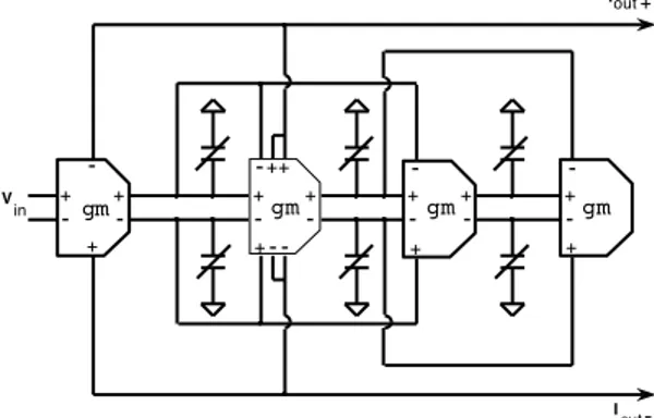
allpass continuous-time filter, both capable of implementing the adaptive forward equalizer. The proposed 3rd order state-space allpass filter is represented in figure 5.
A simpler equivalent 2nd order system was also designed and simulated. Both designs feature very high frequency, low power consumption and low supply voltage using adaptive state-space recursive filters based on current-mode gm-C structures. The filters operate in current-mode so that the outputs of these filters are added in the current summing node that precedes the sampling switch. The adaptation process depends on the generation of the error signal estimated by the difference between the prediction value at the input of the slicer and the data decision at its output. The state-space system is expressed by matrix equation
[ ] [ ] [ ] [ ]
[ ] [ ]
⎪
⎩
⎪
⎨
⎧
⋅
+
⋅
=
⋅
+
⋅
=
• in T out ini
D
i
C
i
i
B
i
A
i
(5)where the system matrices corresponding to the proposed gm-C filter topology of this 3rd order forward equalizer are given by
[ ] [ ] [ ] , 1 0 0 2 , 0 0 , 0 0 0 0 0 0 2 2 1 1 1 1 0 0 0 0 − = ⎥ ⎥ ⎥ ⎥ ⎦ ⎤ ⎢ ⎢ ⎢ ⎢ ⎣ ⎡ = ⎥ ⎥ ⎥ ⎥ ⎥ ⎦ ⎤ ⎢ ⎢ ⎢ ⎢ ⎢ ⎣ ⎡ = ⎥ ⎥ ⎥ ⎥ ⎥ ⎦ ⎤ ⎢ ⎢ ⎢ ⎢ ⎢ ⎣ ⎡ − − − = C D C gm B C gm C gm C gm C gm C gm A
and hence the allpass system transfer function is given by
3 2 2 0 2 1 2 2 1 0 3 3 2 2 0 2 1 2 2 1 0 3 ) ( ) ( ) ( gm gm C C S gm C C S C C C S gm gm C C S gm C C S C C C S s H + + + + + + − + − =
.
(6)The transconductors employed in the filters are low-mismatch high bandwidth balanced pseudo-differential tranconductance cells proposed in [14-15] and are capable of maintaining the correct operation of the filter for supply voltages as low as 1.8V. The variable capacitors are implemented using polarized MOSFET capacitor arrays used as integrating capacitors. Each integrating capacitor C is dimensioned to permit the desirable placement of the poles allowing process tolerances that influence the actual value of gms and of the integrating capacitors, and including the parasitic input capacitance of the gms for very high frequency operation. The DC voltage inherent to the simulated structures biases these transistors well beyond their threshold voltage for enhanced linearity behavior. In both filters we used 4-bit capacitor arrays biased of 12.5fF unit size cells that can be
+ -Forward Equalizer Backward Equalizer e k
Data in Dataout
gm gm gm gm -+ + + + + + + + - -- - -- - - - -+ +- - + + ++ I I in out out V Dat a out Forwar d Equalize r Dat a in + + - Backwar d Equalize r
Figure 3. Decision feedback equalization read channel block diagram
.
Figure 5. Third order allpass forward equalizer
switched on and off by the adaptive control logic. The adaptation process is assumed to be done during the clock recovery preamble and be stable at the decision instants. Alternatively the capacitor array can be loaded in parallel and subsequently adapted to optimum values. Considering equal-valued transconductors with a nominal value of 60µS we used C0 = 0.102pF, C1 = 0.49pF, C2 = 1.77pF nominal values
for the integrating capacitors, matching the theoretical work [13] for the ideal pole locations of the forward equalizer on a third order filter. An identical procedure was followed to calculate the ideal integrating capacitors and corresponding pole location values for the second order allpass filter. The nominal transconductance value was designed to set the size and values of the integrating capacitors in a usable range in a solid state IC, whilst obtaining very low power consumption working at very high frequency. This also implied avoiding the increase of die area due to big capacitor values (e.g. for C2) and
avoiding small capacitor values (e.g. for C0) from getting to
close to the parasitic capacitance of the transconductor cell. IV. SIMULATION RESULTS
Transistor level AC simulations of both allpass equalizers with nominal integrating capacitance values closely match the ideal amplitude and phase characteristics of the allpass filters up to 1GHz, whilst allowing independent pole tuning. The corresponding transient responses to a dibit input was simulated using measured data from a magnetic read head for two consecutive flux transitions with ISI. Figure 6 depicts the equalized transient response of the second order filter and of the third order filter. The differential output closely matches the ideally predicted values, hence the results are nearly superimposed with the ideal response of each of the two equalizers. The simulated power consumption for the 3rd order is 3mW and the power consumption for the 2ndorder equalizer is 2mW, whereas both equalizers have a total die area of less than 0.1mm2.
Figure 6. Dibit-response of the 2nd order
and 3rd order allpass equalizers
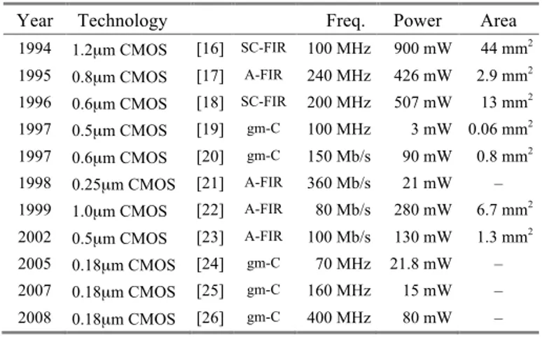
Table 3 comprises several equalizers proposed for implementation the forward equalizer in PRML and DFE read channels.
Table 3. Equalizer performance
Year Technology Freq. Power Area
1994 1.2µm CMOS [16] SC-FIR 100 MHz 900 mW 44 mm2 1995 0.8µm CMOS [17] A-FIR 240 MHz 426 mW 2.9 mm2 1996 0.6µm CMOS [18] SC-FIR 200 MHz 507 mW 13 mm2 1997 0.5µm CMOS [19] gm-C 100 MHz 3 mW 0.06 mm2 1997 0.6µm CMOS [20] gm-C 150 Mb/s 90 mW 0.8 mm2 1998 0.25µm CMOS [21] A-FIR 360 Mb/s 21 mW – 1999 1.0µm CMOS [22] A-FIR 80 Mb/s 280 mW 6.7 mm2 2002 0.5µm CMOS [23] A-FIR 100 Mb/s 130 mW 1.3 mm2 2005 0.18µm CMOS [24] gm-C 70 MHz 21.8 mW – 2007 0.18µm CMOS [25] gm-C 160 MHz 15 mW – 2008 0.18µm CMOS [26] gm-C 400 MHz 80 mW – V. CONCLUSIONS
In this paper we presented two fully analog continuous-time integrated adaptive filters for the implementation of an allpass forward equalizer for MDFE in hard disk drive read-channels. Both current mode state-space recursive filters where simulated at transistor level showing equivalent equalization response to partial response systems, whilst reducing consumption by a factor of 10 to 100 compared to conventional FIR digital equalizers. LMS modified algorithms allowing the automatic tuning of the poles frequency can compensate process tolerances that influence the effective value of the active devices and capacitors. Both equalizers are implemented using current mode continuous-time gm-C filters operating at very high frequency combined with biased MOSFET capacitor arrays in standard digital CMOS technology with low supply voltage.
REFERENCES
[1] R. D. Yamasaki et al., “A 72Mb/s PRML Disk-Drive Channel Chip with an Analog Sampled-Data Signal Processor”, ISSCC Digest of Technical Papers, pp. 278-279, Feb. 1994.
[2] R. Richetta et al., “A 16MB/s PRML Read/Write Data Channel”, ISSCC Digest of Tech. Papers, pp. 78-79, 1995.
[3] G. Tuttle et al., “A 130 Mb/s PRML Read/Write Channel with Digital-Servo Detection”, ISSCC Digest of Tech. Papers, pp. 64-65, 1996. [4] S. Mita et al., “A 150 Mb/s PRML Chip for Magnetic Disk Drives”,
ISSCC Digest of Tech. Papers, pp. 62-63, 1996.
[5] K. Parsi et al., “A 200Mb/s PRML Read/Write Channel IC”, ISSCC Digest of Technical Papers, pp. 66-67, 1996.
[6] P. Pai, A. Brewster, A. Abidi, “A 160MHz End IC for EPR-IV PRML Magnetic-Storage Read Channel” ISSCC Digest of Tech. Papers, pp. 68-69, 1996.
[7] I. Mehr and D. Dalton, “A 500-MSample/s, 6-bit Nyquist-rate ADC for disk-drive read-channel applications”, IEEE J. Solid-State Circuits, vol.34, no.7, pp. 912-920, Jul 1999.
[8] T. Yamamoto et al., “A mixed-signal 0.18-µm CMOS SoC for DVD systems with 432-MSample/s PRML read channel and 16-Mb embedded DRAM” IEEE J. Solid-State Circuits, vol.36, no.11, pp.1785-1794, Nov 2001.
[9] G. Koo, “A robust PRML read channel with digital timing recovery for multi-format optical disc”, Proc. IEEE ISCAS, vol. 4, pp. 21-24, May 2006.
[10] N. Sands et al., “A 200Mb/s Analog DFE Read Channel”, ISSCC Digest of Tech. Papers, pp. 72-73, 1996.
dibit 2nd order
(ideal & simul.) 3rd order (ideal & simul.)
[11] J. Brown, P. Hurst, B. Rothenberg, S. Lewis, "A CMOS adaptive continuous-time forward equalizer, LPF, and RAM-DFE for magnetic recording," IEEE J. Solid-State Circuits, vol.34, no.2, pp. 162-169, Feb 1999.
[12] J. Kenney, L. Carley and R. Wood, “Multi-level Decision Feedback Equalization for Saturation Recording”, IEEE Trans. on Magn., vol. 29, no. 3, pp. 2160-2171, Jul. 1993.
[13] P. McEwen and J. Kenney, “Allpass Forward Equalizer for Decision Feedback Equalization”, IEEE Trans. on Magn., vol. 31, no. 6, pp. 3045 3047, Nov. 1995.
[14] N. Garrido and J. Franca, “An Auto-Biased 0.5µm CMOS Transconductor for Very High Frequency Applications”, Proc. IEEE ISCAS, vol. 1, pp. 325 328, Jun. 1998.
[15] N. Garrido and J. Franca, “A Continuous-Time Area Detector Servo Demodulator for Hard Disk Drives”, Proc. IEEE ICECS, vol. 2, pp. 127 130, Sept. 1998.
[16] G. Uehara and P. Gray, “A 100MHz Output Rate Analog-to-Digital Interface for PRML Magnetic-Disk Read Channels in 1.2µm CMOS”, ISSCC Digest of Tech. Papers, pp. 280-281, 1994.
[17] L. Thon et al., “A 240 MHz 8-Tap Programmable FIR Filter for Disk-Drive Read Channels”, ISSCC Digest of Tech. Papers, pp. 82-83, 1995.
[18] D. Xu, Y. Song and G. Uehara, “A 200MHz 9-Tap Analog Equalizer for Magnetic Disk Read Channels in 0.6µm CMOS”, ISSCC Digest of Tech. Papers, pp. 74-75, 1996.
[19] N. Garrido, J. Franca, and J. Kenney, “A Comparative Study of Two Adaptive Continuous-Time Filters for Decision Feedback Equalization Read Channels”, Proc. IEEE ISCAS, vol. 1, pp. 89-92, Jun. 1997. [20] I. Mehr, “A CMOS continuous-time Gm-C filter for PRML read channel
applications at 150 Mb/s and beyond”, IEEE J. Solid-State Circuits, vol.32, no.4, pp. 499-513, Apr 1997.
[21] L. Thon, “540MHz 21mW MDFE Equalizer and Detector in 0.25µm CMOS”, ISSCC Digest of Tech. Papers, pp. 382-383, Feb. 1998. [22] J. Brown, P. Hurst, B. Rothenberg and S. Lewis, "A CMOS adaptive
continuous-time forward equalizer, LPF, and RAM-DFE for magnetic recording," IEEE J. Solid-State Circuits, vol.34, no.2, pp. 162-169, Feb 1999.
[23] M. Le, P. Hurst, J. Keane, "An adaptive analog noise-predictive decision-feedback equalizer," IEEE J. Solid-State Circuits, vol.37, no.2, pp. 105-113, Feb 2002.
[24] M. Qureshi, P. Allen, "70 MHz CMOS gm-C IF filter" Proc. IEEE ISCAS, vol., no., pp. 5946-5949 Vol. 6, May 2005.
[25] X. Zhu; Y. Sun; J. Moritz, "A 0.18µm CMOS 9mW current-mode FLF linear phase filter with gain boost," Proc. IEEE. MWSCAS, pp. 1517-1520, Aug. 2007.
[26] X. Zhu; Y. Sun; J. Moritz, "A CMOS 80mW 400MHz seventh-order MLF FLF linear phase filter with gain boost," Proc. IEEE ICECS, pp.300-303, Sept. 2008.