B-N Codoped p Type ZnO Thin Films for Optoelectronic Applications
Nripasree Narayanana, Nangarath Kannoth Deepaka*
Received: July 05, 2017; Revised: October 13, 2017; Accepted: October 25, 2017
The success of codoping by donor-acceptor impurities in accomplishing p type ZnO thin films deposited
by spray pyrolysis technique is reported here. Monodoping ZnO with N altered the conductivity type but the resistivity is too high making it practically impossible to be useful in optoelectronic applications. B-N codoping increased the carrier concentration and obtained comparatively low resistivity because codoping enhanced the acceptor incorporation by forming acceptor-donor-acceptor complex in the band gap. XRD analysis revealed the dependence of dopant incorporation on the texture and microstructure
of the films. XPS analysis confirmed the enhancement of N incorporation with codoping. Energy gap value increased for codoped films due to the Burstein-Moss effect, arising from the increase in carrier concentration. Hence the present work envisages the preparation of transparent p type ZnO thin films suitable for tandem thin film solar cells and also for other optoelectronic applications.
Keywords: ZnO, B-N codoping, p type, Burstein-Moss effect, tandem thin film solar cells.
*e-mail: [email protected]
1. Introduction
Transparent conducting oxides (TCOs) are a unique class of materials with wide energy band gap and tunable electrical conductivity from insulating via semiconducting to conducting. This blending of the two conjugate properties - optical transparency and high electrical conductivity - made
thin films of these materials suitable for modern device applications like thin film solar cells1, optical waveguides2,
light emitting diodes3, thin film transistors4, gas sensors5,
etc. Because of low-cost, abundance, less-toxicity and biocompatibility, materials researchers prefer zinc oxide (ZnO) as the most prominent candidate. In addition, the optical energy gap and electrical conductivity of ZnO can
be modified respectively by alloying or doping with suitable
materials.
ZnO is intrinsically n type semiconductor (energy gap ~ 3.37eV) due to the presence of zinc interstitials or oxygen vacancies and is not amenable to both types doping and thus it is harder to develop p type ZnO. This is mainly due to
problems such as its self compensating effect, deep acceptor
levels and low solubility of acceptor dopants6. Codoping of
ZnO with group III and group V elements can be utilized to improve the acceptor solubility and thereby making acceptor levels shallower7. A few reports are available in
the literature studying the feasibility of Al-N codoping8,
In-N codoping9-11, B-N codoping12, Ga-N codoping13, Ag-N
codoping14, Sn-N codoping15 etc. in order to improve the p type electrical performance of ZnO thin films. Thus in the
present study we propose the deposition of B-N codoped
p type thin films of ZnO by spray pyrolysis to be useful in the field of optoelectronics. In tandem thin film solar cells, the efficiency can be improved by stacking absorbers with different energy gap to utilize the entire solar spectrum. But
the main problem associated with this is the requirement of interconnecting contacts of both n and p types, highly transparent to lower energy photons. Thus in the present study, we tried to develop highly transparent and conducting
p type ZnO thin films. To accomplish p type electrical conductivity, ZnO thin films were codoped with boron (B)
and nitrogen (N). Among the various deposition techniques, we opted chemical spray pyrolysis because of its easiness in accomplishing doping during the preparation of precursor solution by simply adding the salts of the desired dopant. In spray deposition, there is no need of vacuum at any stage of preparation and is feasible for large area deposition. Moreover, it is simple, low cost and versatile.
2. Materials and Methods
B-N codoped ZnO thin films with varying B concentration
(0 - 4 at%) were deposited on glass substrates by spray
pyrolysis method. Prior to film deposition, the substrates
were cleaned in solutions of diluted chromic acid, sodium hydroxide and acetone followed by ultrasonic bath cleaning with hot distilled water. Zinc acetate dihydrate [Zn(CH3COO)2 2H2O], ammonium acetate [NH4C2H3O2] and boric acid [H3BO3] were used as the sources of Zn, N and B respectively. A mixture of methanol, deionized water and acetic acid taken in the proportion 65:30:5 plays the role of solvent for the preparation of stock solution. Concentration of the precursor
solution was kept fixed at 0.4M and the N:Zn proportion of
aDepartment of Physics, School of Pure & Applied Physics, Kannur University, Payyanur Campus,
2:1 was maintained for all the samples while the B doping concentration was varied from 0 - 4 at %. In our previous study16, we investigated the impact of N doping with different
N/Zn ratio (0 - 3) on the various physical properties of ZnO
thin films deposited on glass substrates by spray pyrolysis
technique and optimized the N:Zn ratio as 2:1 because that particular sample possessed better optoelectronic properties
compared to others. So we extended the investigation by fixing the particular doping percentage for N salt and
tried to improve the acceptor solubility by adding donor
dopants also at different concentrations. Equivalent masses
of relevant salts were added to the solvent to achieve the desired composition and the resulting solutions were then continuously stirred with a hot magnetic stirrer for 30
minutes at a temperature of about 60ºC. After filtering, these
solutions were sprayed over the glass substrates which were kept on a hot plate maintained at 400 ± 10 ºC to obtain B-N
codoped ZnO thin films.
The structural mapping of the as-deposited films were done by using Rigaku Miniflex 600 X-ray Diffractometer
with CuKα radiation of wavelength, λ = 1.5406 Å. The morphological and composition analyses were performed
with JEOL Model JSM - 6390 scanning electron microscope
operated at 20keV. The elemental composition analysis was carried out using X-ray photoelectron spectroscopy (Thermo
Fisher Scientific). The optical transmission measurement was
done with Jasco V-650 double beam spectrophotometer. The spectra were recorded in the 300-900 nm spectral region.
The electrical properties were measured by the Van der Pauw method using the Hall measurement system (Ecopia Hall Effect Measurement System) with a magnetic field strength
of 0.55T at room temperature. For the measurement, we prepared 1cm×1cm samples and the contacts were made at the four corners of each sample. Highly conducting silver paste was used to make ohmic contacts at the four corners
in the Van der Pauw geometry. These contacts were then
properly heated and allowed to dry to carry out electrical
characterization. Thickness of the deposited films was determined by the gravimetric method (Schimadzu AY 220 Model Balance) and also by using Stylus Profilometer
(Dektak 150).
3. Results and Discussion
3.1. Structural properties
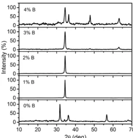
XRD pattern of the prepared thin films were shown in Fig.
1. The samples have no deviation from the hexagonal wurtzite
geometry (JCPDS Card No. 36-1451) so that these films are
monophasic indicating successful incorporation of dopants in the ZnO host lattice. Film with 0 at% B (N monodoped) showed a preferential orientation along the (100) plane with diminutive grain growth along (002), (101) and (110) planes. But B-N codoping shifted the preferred orientation along
the c axis, (002) plane normal to the substrate surface. This shift in preferential orientation is related to the inclusion of
new impurities. Up to 3 at% B doping, the films exhibited
extremely strong preferential orientation along the (002)
plane while for 4 at% B doped film, (101), (102) and (103) reflections appeared with comparable intensity in addition to
the preferred orientation so that it is highly polycrystalline. Thus further increase in doping percentage may result in highly polycrystalline or even amorphous materials.
Figure 1. XRD pattern of the spray pyrolysed B-N codoped ZnO
thin films with various B concentrations.
Crystallite size of the prepared samples for the most
intense diffraction peak was calculated using the Scherrer
formula17
(1)
where 0.9 is the value of the shape factor, λ (=1.5406Å) is the wavelength of the X-rays used, β is the full-width at half maximum intensity in radians and θ is the Bragg's angle. The dislocation density (δ) which is a measure of defects in the films can be calculated using the formula given below18
(2)
The calculated values of crystallite size and dislocation
density are presented in Table 1. It is clear that all the films
were nano-structured. The crystallite size increased up to 2 at% B-N codoping and then decreased. The improvement in crystallinity could be due to the highly textured growth of
films along the (002) plane having minimum surface energy
of formation. The deterioration in crystallinity with further increase in B concentration which favoured random growth of crystallites may arise from the defects and disorders
.
cos
D
=
b
0 9
m
i
D
1
2
Table 1. Structural parameters including crystallite size (D), dislocation density (δ), micro-strain (ε), lattice parameters (a and c), unit
cell volume (V), internal relaxation parameter (u) and bond length (bl) of B-N codoped ZnO thin films with various B concentrations.
B Concentration
(%) D (nm) δ (×10
15m-2) ε (×10-3) a (Å) c (Å) V (×10-30m3) u b l(Å)
0 20.91 2.28 6.06 3.2507 5.2364 47.92 0.378 1.98
1 27.73 1.30 4.22 3.2266 5.1981 46.85 0.378 1.96
2 31.99 0.98 3.65 3.2212 5.1923 46.66 0.378 1.96
3 15.18 4.34 7.69 3.2297 5.1923 46.90 0.379 1.97
4 11.63 7.39 10.04 3.2306 5.1923 46.93 0.379 1.97
introduced by the dopants in the ZnO structure by segregating into the non-crystalline region at the grain boundaries19. Also
the observed variation in crystallinity may arise from the
strain suffered by the lattice. The micro-strain developed in the film was evaluated using the relation20
(3)
The calculated values of strain are presented in Table 1 and show a negative correlation with the crystalline size. The lattice parameters (a and c) and unit cell volume (V) for the hexagonal structure can be determined using the relations21
(4)
(5)
The calculated values of a, c and V are summarized
in Table 1. Compared to N monodoped ZnO thin film, the
lattice parameters and unit cell volume decreased due to the successful incorporation of N with lower ionic radius at O sites. The internal relaxation parameter (u) and the bond length (bl) were calculated using the following relations22
(6)
and
(7)
and are summarized in Table 1. The internal relaxation parameter is a measure of the amount by which each atom is displaced with respect to the next along the c-axis and is 0.375 for an ideal wurtzite crystal. From the table we can
conclude that in the deposited films, the atoms are displaced from the ideal configuration due to the addition of impurities.
B-N codoping resulted in decrease in bond length compared to monodoped one due to the incorporation of N at O sites. Also the calculated values of bond lengths are a little longer
than the ideal value (1.93Å) which could be due to the strain suffered by the lattice. Also we can see from the table that the unit cell volume got reduced for B-N codoped films.
tan
4
f
i
b
=
d
a
h
hk
k
c
l
1
3
4
hkl 2 2 2 2 2 2=
+
+
+
Q V
#
&
V
2
3
a c
2=
u
3
1
c
a
21
4
2=
T Y
+
b
l=
cu
3.2. Morphological analysis
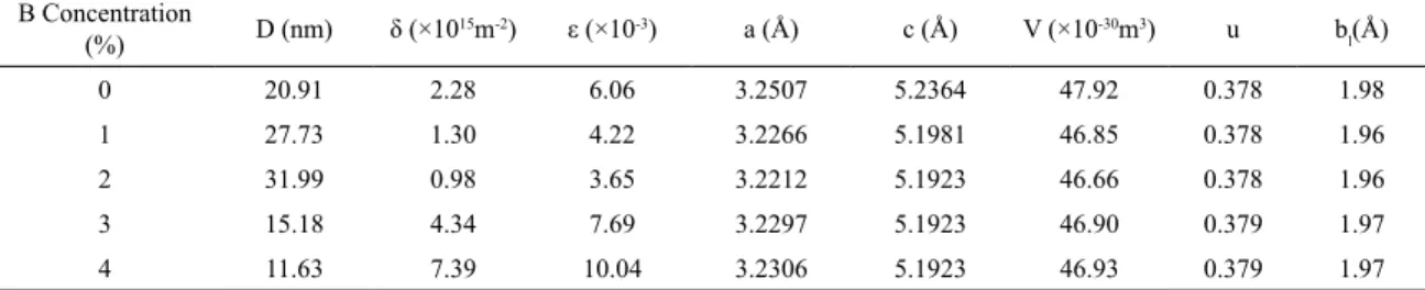
Scanning microscope (SEM) images of the as-deposited thin films are shown in Fig.2. The micrographs showed that all the films had grown uniformly over the substrate surface
without any irregularities. Also the images concluded the
polycrystalline character of the films.
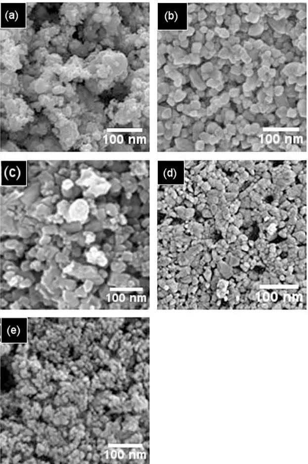
3.3. X-ray photoelectron spectra (XPS) analysis
The XPS analysis results for B-N codoped films are shownin Fig. 3 and the respective chemical composition of various elements are presented in Table 2. The Zn 2p and O 1s core level spectra were similar for all the samples (not shown here). Zn 2p spectra comprises two peaks located around 1020eV and 1040eV corresponding to 2p3/2 and 2p1/2 states respectively. The O 1s peak is centred at around 530eV. The
N1s XPS core level spectra of all the five samples showed
broad peak between 375eV and 430eV binding energy. The deconvolution of the signals using Gaussian function gives
two different peaks. The peaks with lower binding energy are
due to the formation of NO - Zn bond23. The higher binding
energy peak is the characteristic of N2 species occupied at oxygen vacancies24. According to Ozgur et al25, N
O defects
behave as shallow acceptors while N2O as double donor. Thus the balance between these two defects determines the nature
of conductivity in ZnO thin films. The peak centred near
190eV indicates the presence of B - N bonds26. This peak is not seen in the monodoped film's XPS. Thus the observed
enhancement of electrical conductivity can be considered as the consequence of acceptor-donor pair codoping.
3.4. Optical properties
In order to qualify as a transparent conductor, the films
must possess good optical characteristics. Figure 4 shows the optical transmittance spectra of the as-deposited B-N
codoped ZnO thin films. The films, except the N monodoped
one, exhibited better optical transmission in the visible and NIR region. Also all the samples showed sharp fundamental absorption in the near ultraviolet region and undergone a blue-shift of absorption edge with codoping indicating a band gap broadening. In the high transmittance region, the
Figure 3. Core level x-ray photoelectron spectra of N 1s and B 1s states of B-N codoped ZnO thin films with (a) 0, (b) 1, (c) 2, (d) 3
and (e) 4 at% B.
Table 2. Results of XPS analysis
B Concentration (%) Zn (at%) O (at%) N (at%) B (at%)
0 53.24 40.57 6.19 0
1 52.84 33.58 13.58 0.38
2 52.18 32.67 14.24 0.91
3 53.47 29.98 15.41 1.14
4 53.18 29.35 15.64 1.83
films' surface smoothness. Thus N monodoped film's surface
is less smooth and hence lead to increased scattering of photons from the surface itself and poor optical transmittance.
In the case of codoped p type films, there is no significant variation in average transmittance. The film thickness and
refractive index at 633 nm are electronically generated using
PARAV software27 and were presented in Table 3 along with
the experimentally determined thickness values. It can be inferred from the optical transmittance spectra and thickness measurements that the number of peaks and troughs are less
for the comparatively thicker (2 and 4 at% B doped) films.
This is because more peaks and troughs will appear for
thicker films in the higher wavelength region.
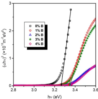
Optical band gaps (Eg) of the deposited thin films are
calculated using the Tauc relation28
(8)
where α is the absorption coefficient, hν energy of photon,
B is the band tailing parameter and n is a constant equal to
1/2 as ZnO is a direct band material. The plots of (αhν)2 versus (hν) for the films were shown in Fig. 5. From the figure, we can make a conclusion that the films are of direct
band gap since the plots are linear near the absorption edge. The band gap energies were determined by extrapolating
the linear portion of the graph and finding the intercepts
on the energy axis. The calculated values of energy gap are presented in Table 3.
The estimated band gap of N doped ZnO thin film is
3.269eV. With B-N codoping, the energy gap blue-shifted which
hv
B
hv
E
gnFigure 4. Optical transmittance spectra of the B-N codoped ZnO
thin films deposited by spray pyrolysis technique with various B
concentrations.
Table 3. Estimated values of film thickness (t) by using Profilometer, gravimetric method and using PARAV software, refractive index at 633nm (n), Energy gap (Eg) and Burstein-Moss energy shift (ΔEBM) for the thin films of B-N codoped ZnO with various B concentrations.
Concentration (%)
t (µm)
n Eg(eV) ΔEBM(eV)
Stylus
Profilometer Gravimetric PARAV
0 0.421 0.394 0.357 1.973 3.269 0.011
1 0.357 0.371 0.328 1.935 3.336 0.265
2 0.408 0.419 0.372 1.970 3.347 0.796
3 0.417 0.399 0.363 1.910 3.343 0.829
4 0.410 0.413 0.368 1.992 3.366 0.842
might be due to the increase in carrier (hole) concentration
known as Burstein-Moss effect. The reduced band gap energy
for the monodoped ZnO is due to the incorporation of N atoms in the ZnO lattice which cause merging of impurity band with the valence band8 and is in agreement with earlier
reports29. The magnitude of Burstein-Moss energy shift
arising from the shift of Fermi levels for the samples were calculated and presented in Table 3.
3.5. Electrical properties
Various electrical parameters such as carrier type, carrier concentration, mobility and resistivity of the deposited thin
films obtained from Hall measurement are presented in
Table 4 along with the measurements made after 20 days
of preparation. All the films exhibited p type electrical
conductivity provided by the formation of NO acceptors at O lattice sites. With B-N codoping, hole concentration enhanced by two orders of magnitude compared to N monodoped one and as a result, we obtained a lower resistive p type material. The enhancement of hole concentration with codoping is related to the incorporation of reactive donor codopant which activates the incorporation of N at
Figure 5. Plot of (αhν)2 v/s hν for spray pyrolysed B-N codoped
ZnO thin films with different B concentration for band gap energy (Eg) determination.
oxygen vacancies by changing the chemical states of N30.
Up to 2 at% B doping the carrier mobility monotonously increased and thereafter started to decrease. The observed trend in carrier mobility with doping might be governed by the scattering at grain boundaries, ionized impurities, other defects etc. Further increase in dopant concentration may sometimes cause the excess dopants to segregate at the grain boundaries where they can be considered as defects due to incomplete bonding. These defects can act as carrier traps which localize the free carriers and form a potential energy barrier. The increase in dopant incorporation increases the barrier heights which prevent the motion of carriers from one crystallite to another and thereby immobilize them. Thus in conclusion, we obtained a lowest resistive or highly
conductive p type ZnO thin film with 2at% B-N codoping. Also the films showed higher stability after 20 days.
the acceptors and reduce the Madelung energy and hence ensures the incorporation of acceptors by forming acceptor-donor-acceptor complex in the forbidden gap15. Thus B-N
codoping improves the delocalization of impurity states at the acceptors and stabilizes the ionic charge distribution in the semiconductor. It should be important here that the donor dopant is not the p type killer, but the reactive codopant which activates acceptors.
4. Conclusions
Spray pyrolysis technique is used to deposit thin films
of N monodoped and B-N codoped ZnO with various B
concentrations to achieve good quality p type thin films. All the films were polycrystalline with hexagonal wurtzite
structure and showed no indication of additional phase other
than ZnO and thereby confirmed the mono-phasic nature of the deposited thin films. The optical transmittance of N monodoped ZnO thin film was poor while codoped films
exhibited better transmission in the Vis-NIR region. With B-N codoping, the band gap energy value increased due tothe
Burstein-Moss effect. Hall measurement showed that B-N codoping effectively improved the hole concentration and
hence the electrical conductivity compared to monodoped
film. The enhancement of hole concentration was attributed
to the better substitution of N at O sites by acceptor-donor
pair codoping which was confirmed by the XPS analysis. So we can strongly propose B-N codoping as an effective tool to fulfil the requirements of p type ZnO thin films and
can be practically used as a transparent interconnect layer
in tandem thin film solar cells and also for applications like solid state lighting, photodetectors, thin film transistors, etc.
5. Acknowledgements
One of the authors would like to gratefully acknowledge University Grants Commission (UGC), New Delhi, India
for providing Senior Research Fellowship (SRF).
6. References
1. Chopra KL, Das SR. Thin Film Solar Cells. New York: Springer;
1983.
2. Misra P, Sahoo PK, Tripathi P, Kulkarni VN, Nandedkar RV, Kukreja LM. Sequential pulsed laser deposition of CdxZn1-xO
alloy thin films for engineering ZnO band gap. Applied Physics A. 2004;78(1):37-40.
3. Gao J, Heeger AJ, Lee JY, Kim CY. Soluble polypyrrole as the
transparent anode in polymer light-emitting diodes. Synthetic
Metals. 1996;82(3):221-223.
4. Norris BJ, Anderson J, Wager JF, Keszler DA. Spin-coated zinc
oxide transparent transistors. Journal of Physics D: Applied
Physics. 2003;36(20):L105-L107.
5. Paneva R, Gotchev D. Non-linear vibration behaviour of thin
multi-layer diaphragms. Sensors and Actuators A: Physical. 1999;72(1):79-87.
6. Bian JM, Li XM, Gao XD, Yu WD, Chen LD. Deposition and electrical properties of N-In codoped p-type ZnO films by ultrasonic
spray pyrolysis. Applied Physics Letters. 2004;84(4):541-543.
7. Yamamoto T, Katayama-Yoshida H. Physics and control
of valence states in ZnO by codoping method. Physica B:
Condensed Matter. 2001;302-303:155-162.
8. Lu JG, Ye ZZ, Zhuge F, Zeng YJ, Zhao BH, Zhu LP. p-type conduction in N-Al co-doped ZnO thin films. Applied Physics Letters. 2004;85(15):3134-3135.
9. Chen LL, Lu JG, Ye ZZ, Lin YM, Zhao BH, Ye YM, et al. p-type behaviour in In-N codoped ZnO thin films. Applied Physics Letters. 2005;87(25):252106.
10. Duta M, Mihaiu S, Munteanu C, Anastasescu M, Osiceanu P, Marin A, et al. Properties of In-N codoped p-type ZnO nanorods
grown through a two-step chemical route. Applied Surface
Science. 2015;344:196-204.
11. Sahu R, Gholap HB, Mounika G, Dileep K, Vishal B, Ghara S, et al. Stable p-type conductivity in B and N co-doped ZnO epitaxial thin film. Physics Status Solidi B. 2016;253(3):504-508.
Table 4. Carrier type, concentration (p), mobility (µ) and resistivity (ρ) obtained from Hall effect measurement for the thin films of B-N
codoped ZnO with various B concentrations along with measurements after 20 days.
Time of Measurement
B Concentration
(%) Type p (cm
-3) µ (cm2/Vs) ρ (Ωcm)
As-deposited
0 p 1.01×10¹⁶ 6.96 8.85×101
1 p 1.13×10¹⁸ 10.24 5.71×10⁻¹
2 p 5.89×10¹⁸ 12.86 8.54×10⁻²
3 p 6.27×10¹⁸ 2.89 3.72×10⁻¹
4 p 6.41×10¹⁸ 1.05 9.41×10⁻¹
After 20 Days
0 p 9.41×10¹⁵ 5.24 1.11×10²
1 p 1.04×10¹⁸ 10.32 6.04×10⁻¹
2 p 4.97×10¹⁸ 12.14 1.09×10⁻¹
3 p 5.21×10¹⁸ 2.45 4.92×10⁻¹
12. Shtereva K, Flickyngerova S, Tvarozek V, Novotny I, Kovac
J, Vincze A. Characterization of gallium-nitrogen co-doped
zinc oxide thin films prepared by RF diode sputtering. Vacuum. 2012;86(6):652-656.
13. Li W, Kong C, Qin G, Ruan H, Fang L. p-Type conductivity and stability of Ag-N codoped ZnO thin films. Journal of Alloys and Compounds. 2014;609:173-177.
14. Nripasree N, Deepak NK. Structural, optical and electrical properties of Sn-N codoped p type ZnO thin films prepared
by spray pyrolysis technique for diode applications. Materials
Science and Engineering: B. 2016;211:121-127.
15. Sahay PP, Tewari S, Nath RK, Jha S, Shamsuddin M. Studies
on ac response of zinc oxide pellets. Journal of Materials
Science. 2008;43(13):4534-4540.
16. Narayanan N, Deepak NK. Impact of N doping on the physical
properties of ZnO thin films. Surface Review and Letters. 2017.
DOI: http://dx.doi.org/10.1142/S0218625X1850035X 17. Ravichandran K, Philominathan P. Investigations on microstructural
and optical properties of CdS films fabricated by a low-cost, simplified spray technique using perfume atomizer for solar
cell applications. Solar Energy. 2008;82(11):1062-1066.
18. Bilgin V, Kose S, Atay F, Akyuz I. The effect of substrate
temperature on the structural and some physical properties of
ultrasonically sprayed CdS films. Materials Chemistry and Physics. 2005;94(1):103-108.
19. Ben Ayadi Z, El Mir L, Djessas K, Alaya S. The properties of aluminum-doped zinc oxide thin films prepared by rf-magnetron
sputtering from nanopowder targets. Materials Science and
Engineering: C. 2008;28(5-6):613-617.
20. Klung HP, Alexander LE. X-Ray Diffraction Procedures: For Polycrystalline and Amorphous Materials. 2nd ed. New York: Wiley; 1974. 992 p.
21. Kim S, Nam G, Park H, Yoon H, Lee SH, Kim JS, et al. Effects of Doping with Al, Ga, and In on Structural and Optical Properties
of ZnO Nanorods Grown by Hydrothermal Method. Bulletin
of the Korean Chemical Society. 2013;34(4):1205-1211.
22. Huang H, Zhao Q, Hong K, Xu Q, Huang X. Optical and
electrical properties of N-doped ZnO heterojunction photodiode.
Physica E: Low-dimensional Systems and Nanostructures. 2014;57:113-117.
23. Zhang JP, Zhang LD, Zhu LQ, Zhang Y, Liu M, Wang XJ, et al. Characterization of ZnO:N films prepared by annealing sputtered zinc oxynitride films at different temperatures. Journal of Applied Physics. 2007;102(11):114903.
24. Ӧzgür Ü, Alivov YI, Liu C, Teke A, Reshchikov MA, Doğan S,
et al. A comprehensive review of ZnO materials and devices.
Journal of Applied Physics. 2005;98(4):041301.
25. Laidani N, Anderle M, Canteri R, Elia L, Luches A, Martino M, et al. Structural and compositional study of B-C-N films
produced by laser ablation of B4C targets in N2 atmosphere.
Applied Surface Science. 2000;157(3):135-144.
26. Shinde SS, Shinde PS, Oh YW, Haranath D, Bhosale CH, Rajpure KY. Investigation of structural, optical and luminescent properties of sprayed N-doped zinc oxide thin films. Journal of Analytical and Applied Pyrolysis. 2012;97:181-188.
27. Ganjoo A, Golovchak R. Computer program PARAV for calculating optical constants of thin films and bulk materials: Case study
of amorphous semiconductors. Journal of Optoelectronics and Advanced Materials. 2008;10(6):1328-1332.
28. Ohta Y, Haga Y, Abe Y. Crystallographic features of ZnO
single crystals. Japanese Journal of Applied Physics.
1997;36:L1040-L1042.
29. Dhara S, Giri PK. Stable p-type conductivity and enhanced
photoconductivity from nitrogen-doped annealed ZnO thin
film. Thin Solid Films. 2012;520(15):5000-5006.
30. Yan Z, Song ZT, Liu WL, Wan Q, Zhang FM, Feng SL. Optical and electrical properties of p-type zinc oxide thin films