67
FABRICATION AND EVALUATION OF CuO/ZnO
HETEROSTRUCTURES FOR PHOTOELECTRIC CONVERSION
Hiroki Kidowaki, Takeo Oku& Tsuyoshi Akiyama Department of Materials Science, The University of Shiga Prefecture,
2500 Hassaka, Hikone, Shiga 522-8533 Japan
*
E-mail: oku@mat.usp.ac.jp
ABSTRACT
Cuprous oxide (CuO)-based solar cells with zinc oxide (ZnO) were fabricated on indium tin oxide by an electrodeposition. Microstructure and cell performance of the solar cells with ITO/CuO/ZnO or ITO/ZnO/CuO structures were investigated. Photovoltaic devices based on the CuO/ZnO or ZnO/CuO heterojunction structures provided photovoltaic properties under illumination. Structural, morphological and absorption measurement of the CuO/ZnO heterojunction were studied by using X-ray diffraction, transmission electron microscopy and light current-voltage characteristics. The energy levels of the present solar cells were also discussed.
Keywords: copper oxide, thin film, solar cell, photovoltaic property, optical property
1. INTRODUCTION
Solar cell technology for future energy resources has been progressed recently. Silicon is used as the semiconductor material for conventional solar cells, and the cost reduction of the solar cells is one of the most important issues. Cu oxides such as CuO and Cu2O are one of the candidate materials. The features of copper oxide semiconductors are
high optical absorption coeffcient and non toxicity and low cost fabrication [1,2]. CuO and Cu2O are p-type
semiconductors with band gaps of ~1.5 eV and ~2.0 eV, respectively, which are close to the ideal energy gap for solar cells and allows for good solar spectral absorption due to these direct band gap. The highest efficiency of ~2% for Cu2O solar cells has been obtained by using the high-temperature annealing method and an expensive vacuum
evaporation technique [3]. Efficient heterojunction solar cells with p-Cu2O and n-ZnO fabricated by
electrodeposition and photochemical deposition methods have been investigated and reported [4,5].
However, the solar cells with a CuO/ZnO structure have not been reported. Since the ideal energy band gap for solar cells is ~1.4 eV, CuO could be an ideal material for solar cells. The purpose of the present work is to fabricate and characterize solar cells with CuO/ZnO structures. The heterojunction solar cells were denoted as CuO/ZnO. ZnO is an n-type semiconductor with a wide band gap of ~3.37 eV, which can be applied to solar cells [6].
2. EXPERIMENTAL
CuO layers were prepared on pre-cleaned indium tin oxide (ITO) glass plate by electrodeposition using platinum as counter electrode. Copper(II) sulfate (CuSO4, 0.4 mol/L, Wako 97.5%) and l-lactic acid (3 mol/L, Wako) were
dissolved into distilled water. pH of the electrolyte solution was adjusted to 12.5 by adding NaOH.
Figure 1: Structure of (a) ITO/CuO/ZnO/Al and (b) ITO/ZnO/CuO/Al solar cells.
Al
ZnO
CuO
ITO
Glass
-
(a)
+
Al
CuO
ZnO
ITO
Glass
-
(b)
68
The temperature of electrolyte solution was kept at 65 °C during electro deposition. Preparation of CuO layers were carried out at voltages of +0.70 V and quantity of electric charge of 2.2 C cm-2. After the deposition, the sample was rinsed with water and transferred into the ZnO electro deposition bath. ZnO layers were electro-doposited from 0.025 M aqueous solution of Zn(NO3) on the ITO/CuO substrate. The sample thickness ranged between 1 and 2 m
depending on the deposition time and current. Finally, the substrates were rinsed with water, dried with air and quickly transferred into a thermal evaporator for the vacuum deposition of the aluminum (Al) back contact. Structure of heterojunction solar cells were denoted as ITO/CuO/ZnO/Al, with a schematic illustration as shown in Fig. 1
Current density-voltage (J-V) characteristics (Hokuto Denko Corp., HSV-100) of the solar cells were measured using potentiostat (Hokuto Denko, HSV-100) in the dark and under illumination at 100 mW/cm2 by using an AM 1.5 solar simulator (San-ei Electric, Electric, XES-301S). The solar cells were illuminated through the side of the ITO substrate, and the illuminated area was 0.16 cm2. Optical absorption of the solar cells was investigated by means of UV visible spectroscopy (Hitachi, Ltd., U-4100). Microstructures of the copper oxides were investigated by X-ray diffractometer (XRD, PHILIPS X’Pert-MPD System) with CuKα radiation operating at 40 kV and 40 mA. Transmission electron microscopy (TEM, Hitachi H-8100, 200 kV operating voltage) was also carried out for nanostructure analysis.
3. RESULTS AND DISCUSSION
The CuO/ZnO structure showed characteristic curves with short-circuit current and open-circuit voltage. Table 1 shows measured parameters of CuO-based solar cells. A solar cell with a CuO/ZnO structure provided a power
conversion efficiency ( ) of 1.1×10⁻⁴
%, fill factor (FF) of 0.25, short-circuit current density (Jsc) of 1.9 mAcm-2 and
open-circuit voltage (Voc) of 2.8 × 10⁻⁴ V. Figure 2 shows measured optical absorption of thin films. The CuO thin
film shows high optical absorption in the range of 400 nm and 700 nm.
Table 1: Measured parameters of CuO-based solar cells
Figure 2: UV-visible absorption spectra of thin films prepared by electrodeposition.
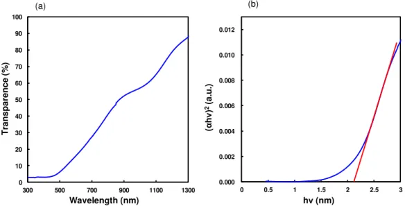
Transmittance spectrum of 100 nm thick CuO film, deposited on ITO, is presented in Fig. 3(a). From this spectrum, the optical absorption coefficients (α) of this film was determined from the spectral transmittance using the next
equation, α = 1/d・ln(1/T). Where d is the film thickness and T is the transmittance [7]. For determination of the
optical band gap energy (Eg), the method based on the relation of αh = A(h -Eg)n/2 was used, where n is a number
that depends on the nature of the transition. In this case, its value was found to be 1, which corresponds to direct
0.0 0.2 0.4 0.6 0.8 1.0 1.2 1.4 1.6
300 400 500 600 700 800
Wavelength (nm)
A
b
s
o
rb
a
n
c
e
CuO
ZnO
Voc (V) Jsc (mA cm-2) FF (%)
CuO (5 min)/ZnO 2.8×10⁻⁴ 1.9 0.25 1.1×10⁻⁴
CuO (10 min)/ZnO 1.8×10⁻⁴ 0.017 0.25 1.1×10⁻⁷
69
band to band transition. Figure 3(b) is a Tauc plot, which shows (αhν)2 versus hν for the CuO film. The intersection
of the straight line with the h -axis determines the optical band gap energy Eg [8]. It was found to be ~2.1 eV which
is wider than the ideal band gap of the CuO crystal.
Figure 3: (a) Optical transmission spectrum of 100 nm thick CuO film, and (b) Tauc plot for the CuO thin film.
Figure 4: (a) Optical transmission spectrum of 100 nm thick ZnO film, and (b) Tauc plot for the ZnO thin film.
All the crystalline components in the CuO and ZnO thin films were investigated by XRD, as shown in Fig. 5. Diffraction peaks corresponding to CuO and ZnO are observed in thin films, which consisted of cupric phase with monoclinic system (space group of C2/c). The particle size was estimated using Scherrer’s equationμ D= 0.λ /Bcos ,
where , B, and represent the wavelength of the X-ray source, the full width at half maximum (FWHM), and the
Bragg angle, respectively [9]. The crystallite sizes of CuO and ZnO were determined to be 49.0 nm and 82.0 nm, respectively. Lattice constants of CuO and ZnO were summarized as listed in Table 2 and Table 3, comparing with reported values [10,11]. From the lattice constants, the crystal structures of CuO and ZnO have some crystal distortions. This would result in charge carriers transport in a reverse direction through the device [12], resulting in recombination. To increase the efficiency of the CuO/ZnO solar cells, small grain size of ZnO and higher crystallinity of CuO would be necessary.
0 10 20 30 40 50 60 70 80 90 100
300 500 700 900 1100 1300
0.000 0.002 0.004 0.006 0.008 0.010 0.012
0 0.5 1 1.5 2 2.5 3
Wavelength (nm) Tra ns pa re nc e ( % )
hν(nm)
( α h ν ) 2(a .u .) (a) (b) 0.00 0.01 0.01 0.02 0.02 0.03 0.03
4.20 4.25 4.30 4.35 0 10 20 30 40 50 60 70
300 400 500 600 700 800
Wavelength (nm) T ra n s m it ta n c e (% )
hν(eV)
70 .
Figure 5: XRD patterns of (a) CuO and (b) ZnO thin films.
Table 2: Lattice parameters of CuO.
a (nm) b (nm) c (nm)
Present data 0.4627 0.3614 0.5254
Previous data [10] 0.4679 0.3426 0.5127
Table 3: Lattice parameters of ZnO
.
a (nm) c (nm)
Present data 0.2816 0.5213
Previous data [11] 0.3257 0.5213
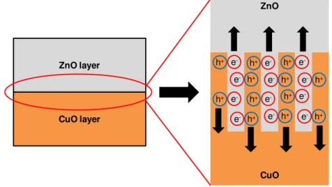
A TEM image and an electron diffraction pattern of CuO prepared by electrodeposition are shown in Fig. 6. Figure 6(a) indicated CuO nanowires with the diameters of 50~60 nm, which agrees with XRD results. Debye-Scherrer rings in Fig. 6(b) indicate microcrystalline structures of CuO. Figures 7 are a TEM image and an electron diffraction pattern of a ZnO layer prepared by electrodeposition. Debye-Scherrer rings in Fig. 7(b) indicate microcrystalline structures of ZnO.
The conversion efficiency of the solar cells depends on morphology of interfaces in solar cells. A schematic microstructure of the present solar cells fabricated by electrodeposition is shown in Fig. 8. The CuO layer has a nanowire structure, and interface area of the p-n junction would be increased, which would result in charge separation at the interface.
Energy level diagram of the CuO/ZnO solar cell is summarized as shown in Fig. 9. Previously reported values were used for the energy levels [9]. It has been reported that Voc is nearly proportional to the band gap of the
semiconductors, and control of the energy level is important to increase efficiency [13].Compared to silicon with an indirect transition band structure, CuO with a direct transition band structure is more suitable for the optical absorption property. In addition, the ultrathin film of the CuO layers could provide efficient charge injection because of the high optical absorption.
20 30 40 50 60 70 20 30 40 50 60 70
ITO
CuO 002
CuO 112
CuO 113
Cu 111
ZnO 002
ZnO 002
ZnO 002
ZnO 002 ZnO 103
(a) (b)
2θ(degree) 2θ(degree)
In
te
n
s
ity
(
a
.u
.)
In
te
n
s
ity
(
a
.u
71
Figure 6: (a) TEM image and (b) electron diffraction pattern of CuO prepared by electrodeposition.
Figure 7: (a) TEM image and (b) electron diffraction pattern of ZnO prepared by electrodeposition.
Figure 8: Schematic microstructure of the present solar cells fabricated by electrodeposition.
70 nm
002
000 110 112 113
b a
000
002 102 103
50 nm
b a
CuO layer ZnO layer
CuO ZnO
e
-h+
e
-h+
e- h+
e- h+
e
-h+
e
-h+
e- h+
e- h+
e
-h+
e
-h+
e- h+
72
Figure 9: Energy level diagram of (a) ITO/CuO/ZnO/Al and (b) ITO/ZnO/CuO/Au inverted solar cells.
4. CONCLUSIONS
ITO/CuO/ZnO/Al solar cells were produced and characterized, which provided η of 1.1×10⁻⁴ %, FF of 0.25, Jsc of
1.6 mAcm-2 and Voc of 2.8×10⁻⁴ V. The CuO/ZnO structure showed high optical absorption in the range of 400 nm
and 700 nm, and the Eg of CuO was found to be ~2.1 eV from the Tauc plot, which is wider than that of the ideal
band gap of the CuO crystal. A crystallite size of CuO was determined to be 49.0 nm, and CuO had a nanowire structure, which would be expected for increase of the efficiency of CuO/ZnO solar cells. Energy level diagram for the CuO/ZnO structure was proposed, and separated holes could transfer from the valence band of the CuO to the ITO, and separated electrons could transfer from the conduction band of the CuO to the Al electrode, respectively. Formation of the CuO/ZnO active layer with homogeneously distributed CuO nanowires would improve the efficiencies of the solar cells. To increase power conversion efficiency, structures of the solar cells should be optimized.
5. REFERENCES
[1] L.C.Olsen, R.C.Bohara, M.W.Urie, Explanation for low-efficiency Cu2O Schottky-barrier solar cells, App.
Phys. Lett. 34 47-50 (1979).
[2] J.Herion, E.A.Niekisch, G.Schari, Investigation of metal oxide/cuprous oxide heterojunction solar cells. Sol. Energy Mater. Sol. cells 4 101-112 (1980).
[3] A.Mittiga, E.Salsa, F.Sarto, M.Tucci, and R.Vasanthi, Heterojunction solar cell with 2% efficiency based on a Cu2O substrate, App. Phys. Lett. 88 163502-163503 (2006).
[4] M.Izaki, K.Mizuno, T.Shinagawa, M.Inaba and A.Tasaka, Photochemical construction of photovoltaic device composed of p-copper(I) and n-zinc oxide, J. Electrochem. Soc. 153 C668-C672 (2006).
[5] M.Izaki, T.Shinagawa, K.Mizuno, Y.Ida, M.Inaba and A.Tasaka, Photochemically constructed p-Cu2O/n-ZnO
heterojunction diode device, J. Phys. D : App. Phys. 40 3326-3329 (2007).
[6] R.Vinodkumar, K.J.Letthy, D.Beena, A.P.Detty, I.Nava, U.V.Nayar, V.P.Mahadevan, V.Ganesan, V.R.Rdddy, Effect of ITO buffer layers on the structural, optical and electrical properties of ZnO multilayer thin films prepared by pulsed laser deposition technique, Sol. Energy. Mater. Sol. Cells 94 68-74 (2010).
[7] J.W.C.Chen, D.C.Perng, J.F.Fang, Nano-structured Cu2O solar cells fabricated on sparse ZnO nanorods, Sol.
Energy. Mater. Sol. Cells 95 2471-2477 (2011)
[8] V.Georgieva, M.Ristov, Electrodeposited cuprous oxide on indium tin oxide for solar applications, Sol. Energy Mater. Sol. Cells 73 67-73 (2002).
[9] T.Oku, T.Noma, A.Suzuki, K.Kikuchi, S.Kikuchi, Fabrication and characterization of fullerene/porphyrin bulk heterojunction solar cells, J. Phys. Chem. Solids 71 551-555 (2009).
[10] M.I.Domnina, S.K.Filatov, I.Zyuzyukia and L.P.Vergasova, Neorgan. Materialy 22 1743 (1986). [11] Albertsson, S.C.Abrahams and Kvick, Acta Cryst. B45 34 (1989).
[12] T.Gershon, Musselman, P.Kevin, A.Marin, Friend, H.Richard, L.MacManus-Driscoll Judith, Thin-film ZnO/Cu2O solar cells incorporating an organic buffer layer, Sol. Energy Mater. Sol. Cells 96 148-154 (2012).
[13] T.Oku, R.Motoyoshi, K.Fujimoto, T.Akiyama, B.Jeyadevan, J.Cuya, Structures and photovoltaic properties of copper oxides/fullerene solar cells, J. Phys. Chem. Solids 72 1206-1211 (2011).
(a) (b)
-4.7 eV 2.1 eV
4.2 eV
-4.3 eV
ITO CuO ZnO Al
e
-h
+-4.7 eV 2.1 eV
4.2 eV
-4.8 eV
ITO CuO ZnO