Mafalda Sofia Fonseca Caldas
Bachelor in Micro and Nanotechnologies Engineering
Stacks of alternating conductive
and non-conductive oxides studied by
ellipsometry
Dissertation submitted in partial fulfilment of the requirements for the degree of
Master of Science in
Micro and Nanotechnologies Engineering
Advisor: Prof. Jan Genoe, Full Professor, University of
Leuven
Co-advisor: Prof. Dra. Elvira Maria Correia Fortunato, Vice-
Rector for Researcher, Nova University of Lisbon
Acknowledgements
It's been 5 years, 5 years that I will never forget, thanks to all of you. To all of you who motivated me and who have always believed in my abilities. And thanks to that I finished my master's degree in Micro and Nanotechnologies Engineering.I would especially like to thank my thesis advisor, Prof. Jan Genoe, my co-advisor, Prof. Elvira Fortunato, and Prof. Paul Heremans for the opportunity given to me to be able to do this in one of the best research centres in the world, imec. Opportunity that opened my horizons and enabled me to be close to all the equipment needed to develop my thesis in the best way possible.
Also to thank Prof. Rodrigo Martins, who together with Professor Elvira Fortunato, founded the course of the future. The course that has always made us dream and believe that someday we will be successful engineers.
To Dr. Robert Gehlhaar, Dr. Manoj Nag, Dr. Cédric Rolin and Dr. David Cheyns for all the help and patience throughout my stay in the one that was my home for 5 months. Without your help nothing would be possible. Not forgetting all the imec LAE group, for all the friendliness and willingness to help whenever needed. Together, you made me feel at home in your home.
To thank my parents for all the encouragement and support, as well as for the education and values transmitted, teachings that have formed as solid foundations to be able to successfully follow the path I have travelled throughout my life and especially during these 5 years. I am also grateful for the understanding of my departure from this last semester and impatience, as well as my two brothers.
To Carolina Leitão and Joana Tavares, because without them nothing would have been the same. With them I shared everything during this 5-year journey. All classes, every afternoon of study, all group work together, but especially the 24 hours of my day during this period abroad. Thank you, thank you and thank you so much for always being there when I need you.
To my friends from Leiria, who have been present in my life since always and who were also present in my academic life, one way or another.
Special thanks to Vladimir, Dieter, Guillaume and Gemma for the friendship for life that was created and to make every day of work, and outside of it, easier and more fun. It was thanks to you and Andrej, the best possible housemate, that Leuven enchanted me in this special way. I also thank Subhobroto, Sheri, Prakhar, Ravi and Majdi, who although I only met better at the end, unfortunately, were fantastic friends. I hope one day I will be able to see you all again and who knows, may it be here in Portugal.
To the faculty and all the professors of it, especially those who were part of my journey, for the availability and commitment to transmit to me and my colleagues the knowledge that we have nowadays.
Finally, I thank all the other people who have passed through my life and who have helped me to go through these 24 years of my life, making me the person I am today.
Abstract
High-quality video-rate holography is a logic evolution of display technology that requests an extraordinary technological effort. Due to this challenge, this has not been demonstrated yet. For this realization it is necessary to vary the refractive index within a waveguide with high precision, subwavelength spatial resolution and GHz frequency. Within this thesis, the development of a metamaterial for the cladding of such a holographic waveguide was the target. This material is supposed to consist of non-optically absorbing materials where an electrical conductor is laterally separated by an insulating material. In our chosen set of materials, we investigated Gallium Indium Zinc Oxide (IGZO), Indium-Tin-Oxide (ITO) and Indium Tin Zinc Oxide (ITZO) as transparent conductive oxides and Silicon Nitride (Si3N4) and Silicon Oxynitride (SiOxNy) as insulatingoxide (IO).
IGZO, a transparent semiconductor oxide (TSO), appeared recently as new material for flexible and transparent thin film transistors. The good electrical conductivity together with high transparency in the visible region (> 80% optical transmittance) at room temperature makes this material a very attractive candidate. ITO is one of the most important transparent conductor oxides (TCOs) that exists. It is applied in different technologies due to its high electrical conductivity and high optical transparency. ITZO has been a promising replacement for ITO as the TCO layer in many opto-electronic applications. The insulator Si3N4 is widely used as a passivation layer, a barrier, or as a
masking layer to prevent oxidation or diffusion in underlying materials in patterned areas, and as a final protection layer to finished devices because of its radiation resistance and hardness. Another candidate, SiOxNy, is a material that has been under investigation
because it can be considered an intermediate between Si3N4 and SiO2 in terms of
physical and chemical properties. Thus, is considered very good for electro-optics and organic light-emitting devices as its properties can be tuned by varying the ratio of the oxide and nitride content.
In this work, we start with describing the production techniques used. All the TSOs were deposited by Direct Current Sputtering, that is a high vacuum physical vapor deposition (PVD) technology. Inductively coupled plasma chemical vapor deposition (ICP-CVD) was the technique used for the deposition of IOs. With the help of ellipsometry it was also possible to determine the optical constants and the thickness of them. Thus, we began by analysing these parameters and, when necessary, altering them in order to approach the main requirements of this project. Finally, several comparative studies on optical properties were carried out to find applicable combinations between the two types of oxide. It was therefore concluded that IGZO is the preferred candidate in combination with SiN or SiON. because of their similar optical constants for certain wavelengths.
In addition, the reliability and sensitivity of ellipsometry were studied to see if this could be used in this application, or whether it was necessary to investigate another method capable of detecting the low optical extinction coefficients of the materials of interest.
Resumo
Holografia de taxa de vídeo de alta qualidade é uma evolução lógica da tecnologia de exibição que requer um extraordinário esforço tecnológico. Devido a esse desafio, ainda não foi demonstrado. Para que isso aconteça, é necessário variar o índice de refração dentro de um guia de onda com alta precisão, resolução espacial de sub-comprimento de onda e frequência de GHz. Nesta tese, o objetivo foi o desenvolvimento de um metamaterial para o revestimento de tal guia de ondas holográfico. Este deve consistir em materiais opticamente não absorventes, onde um condutor elétrico é separado lateralmente por um material isolante. No nosso conjunto de materiais escolhido, investigámos o Óxido de Zinco Gálio Índio (IGZO), Óxido de Índio e Estanho (ITO) e Óxido de Zinco Ìndio e Estanho (ITZO) como óxidos condutores transparentes e Nitreto de Silício (Si3N4) e Oxinitreto de Silício (SiOxNy) como óxido isolante (IO).O IGZO, um óxido semicondutor transparente (TSO), apareceu recentemente como novo material para transístores de filmes finos transparentes e flexíveis. A boa condutividade elétrica, juntamente com alta transparência na região visível (> 80% de transmitância ótica) à temperatura ambiente, torna este material um candidato muito atraente. O ITO é um dos mais importantes óxidos condutores transparentes (TCOs) existente. É aplicado em diferentes tecnologias devido à sua alta condutividade elétrica e alta transparência ótica. Já o ITZO tem sido um substituto promissor para o ITO como camada de TCO em muitas aplicações opto-eletrônicas. Já o isolante Si3N4 é amplamente utilizado como camada de passivação, barreira ou como camada de mascaramento para evitar a oxidação ou difusão em materiais subjacentes em áreas padronizadas e como camada de proteção final para dispositivos acabados devido à sua resistência à radiação e dureza. Outro candidato, o SiOxNy, é um material que está a ser investigado devido a ser considerado um intermediário entre o Si3N4 e o SiO2 em termos de propriedades físicas e químicas. Assim, é considerado muito bom para dispositivos optoelectrónicos e emissores de luz orgânicos, pois as suas propriedades podem ser ajustadas variando a proporção do teor de óxido e nitreto.
Neste trabalho, começou-se por descrever as técnicas de produção utilizadas. Todos os TSOs foram depositados por Sputtering de Corrente Contínua, que é uma tecnologia de deposição física de vapor a alto vácuo (PVD). A deposição química a vapor assistida por plasma de alta densidade acoplado indutivamente (ICP-CVD) foi a técnica utilizada para a deposição dos IOs. Com a ajuda da elipsometria, também foi possível determinar as constantes óticas e a espessura destes. Assim, começou-se por analisar esses parâmetros e, quando necessário, alterá-los para nos aproximarmos dos principais requisitos deste projeto. Finalmente, vários estudos comparativos das propriedades óticas foram realizados para encontrar combinações aplicáveis entre os dois tipos de óxido. Concluiu-se, portanto, que o IGZO é o candidato preferido em combinação com o SiN ou o SiON. devido às suas semelhanças em termos das constantes óticas para certos comprimentos de onda.
Além disso, a confiabilidade e a sensibilidade da elipsometria foram estudadas para verificar se este método poderia ser utilizado nesta aplicação, ou se era necessário investigar outro capaz de detetar os baixos coeficientes de extinção óticos dos materiais de interesse.
Contents
Acknowledgements ... vii
Abstract ... ix
Resumo ... xi
Contents ... xiii
List of Figures ... xv
List of Tables ... xvii
Acronyms ... xix
Motivation and Objectives... xxi
Introduction ... 1
1. Video Holography ... 1
2. Transparent conductive oxides ... 2
3. Transparent semiconductor oxides ... 3
4. Dielectric materials ... 4
Experimental Methods ... 6
1. Deposition of thin films ... 6
1.1 Direct Current Sputtering ... 6
1.2 Inductively coupled plasma chemical vapor deposition (ICP-CVD) ... 6
2. Determination of optical constants ... 7
2.1 Spectroscopic ellipsometry ... 7
Results and Discussion ... 8
3.1 IGZO ... 8
3.2 ITO 10% ... 10
3.3 ITZO ... 11
3.4 SiN and SiON... 12
3.5 Comparison of the refractive indices ... 16
Conclusion and Future Perspectives ... 20
References ... 22
List of Figures
Figure 1- Implementation of the new metamaterial between the silicon wafer and thewaveguide. ... 1 Figure 2- Conditions for transparent and conductive materials: (i) gap energy of more
than 3 eV; ii) carrier concentration less than 1021 cm-3. ... 2
Figure 3- The solar spectrum on earth, sensitivity of the human eye and the properties of transparent and semiconducting materials. ... 3 Figure 4- Schematic setup of the DC Sputtering deposition process. ... 6 Figure 5- Most important parameters of the process that can be controlled in the
deposition. ... 6 Figure 6- The difference in refractive index, between measuring with one (75°) or three
angles (55°, 65°, 75°), as a function of wavelength. ... 8 Figure 7- The difference in extinction coefficient, between measuring with one (75°) or
three angles (55°, 65°, 75°), as a function of wavelength. ... 8 Figure 8- The variation of refractive index with wavelength of various IGZO samples. .. 9 Figure 9- The variation of extinction coefficient with wavelength of various IGZO samples. ... 9 Figure 10- The variation of the extinction coefficient on a logarithmic scale with
wavelength of various IGZO samples. ... 9 Figure 11- The variation of refractive index with O2 concentration, for 3 different
wavelengths, of various IGZO samples. ... 10 Figure 12- The variation of extinction coefficient with O2 concentration, for 3 different
wavelengths, of various IGZO samples. ... 10 Figure 13- The variation of refractive index with thickness, before and after annealing, of
various ITO samples. ... 10 Figure 14- The variation of extinction coefficient on a logarithmic scale with thickness,
before and after annealing, of various ITO samples. ... 10 Figure 15- The variation of refractive index with wavelength, before and after annealing,
of an ITZO sample. ... 11 Figure 16- The variation of extinction coefficient with wavelength, before and after
annealing, of an ITZO sample. ... 11 Figure 17- The variation of refractive index with O2 concentration, for 3 different
wavelengths, of various ITZO samples. ... 12 Figure 18- The variation of extinction coefficient with O2 concentration, for 3 different
wavelengths, of various ITZO samples. ... 12 Figure 19- The variation of refractive index with wavelength of various SiN and SiON
samples. ... 13 Figure 20- The variation of the refractive index with the change in the N2 and N2O
Figure 21- The variation of the refractive index with the change in the N2 and N2O
concentrations to a wavelength of 650 nm. ... 13 Figure 22- The variation of the Tan values normalized with the extinction coefficient
on a logarithmic scale. ... 14 Figure 23- The variation of the Cos values normalized with the extinction coefficient on
a logarithmic scale. ... 14 Figure 24- The variation of the values with wavelength, for angles of incidence that
change between 25 ° and 30 ° and for values of k that change between 0, 1E-4 and 2E-1E-4. ... 15 Figure 25- The variation of the values normalized with wavelength, for angles of
incidence that change between 25 ° and 30 ° and for values of k that change between 1E-4 and 2E-4. ... 15 Figure 26- The variation of the Cos values normalized with the extinction coefficient on
a logarithmic scale. ... 15 Figure 27- The comparison of the refractive index of IGZO and SiN or SiON samples as
a function of wavelength. ... 16 Figure 28- The comparison of the refractive index of ITZO and SiN or SiON samples as
a function of wavelength. ... 17 Figure 29- The comparison of the refractive index of ITO and SiN or SiON samples as a
List of Tables
Table 1- Thickness values of the different samples of IGZO with different O2concentrations, studied for TSO. ... 9 Table 2- Values of the concentration of SiH4, N2 and N2O for the different samples of SiN
Acronyms
a-IGZO amorphous indium gallium zinc oxideAOS amorphous oxide semiconductor
a-TSO amorphous transparent semiconductive oxide CVD chemical vapor deposition
DC sputtering direct current sputtering
IC integrated circuit
ICP-CVD inductively coupled plasma chemical vapor deposition IGZO indium gallium zinc oxide
IO insulating oxide
ITO indium tin oxide
ITZO indium tin zinc oxide PVD physical vapor deposition
SE spectroscopic ellipsometry
SiN silicon nitride
SiON silicon oxynitride
TCO transparent conductive oxide TFT thin-film transistor
Motivation and Objectives
The optical transparency of stacks with alternating conductive (e.g. ITZO and ITO) or semi-conductive (e.g. IGZO) oxides with non-conductive oxides (e.g. SiO2, Si3N4and SiOxNy) enables these stacks to be used in future opto-electronic devices, such as
lasers, optical multiplexers, switchable holograms, etc. Future opto-electronic devices that people have always dreamed about, since they always seemed to be true in the movies.
In order to design these future components, a good understanding of the optical properties of these stacks is essential.
Therefore, the main goal of this work is to deposit planar stacks of alternating optical transparent layers, such as IGZO, ITO, ITZO, SiO2, Si3N4 and SiOxNy and analyse
P
Introduction
In this chapter the concept of Video Holography and how we think it will emerge in the scientific world is explained. Additionally, it explores the materials for that advance, such as, transparent conductive oxides, transparent semiconducting oxides and dielectric materials, and their unique properties.1.
Video Holography
Between 1941 and 1947, Dennis Gabor [1] stated that holography is based on the generation of points in space where the constructive interference of light beams is achieved, by applying local changes to the wave phase. By positioning (in reflection or transmission) a 2-dimensional surface, these local phase changes are obtained. However, the surface contains a pattern which locally affects the phase in the path of the light beam, and by varying the thickness (e.g. imprint) or the local refractive index, these patterns are achieved.
Nowadays, it is known that by using materials those have a controllable refractive index, re-writeable holographic displays can be obtained, which is the focus of our interest [2]. However, there is no technique yet that achieves this controllable refractive index in parallel with the spatial resolution required for the holography and the temporal resolution required for the video rate or higher. This means that there is no known method for performing high-quality video-rate holography.
To make scientific advances lead to an electrically-controlled holographic projection at video rate, materials and methods to dynamically manipulate light traveling in the waveguide into an electrically controllable hologram will be used. In order to control the refractive index at nanoscale and high speed (GHz) it was proposed to elaborate a radically new metamaterial.
Figure 1- Implementation of the new metamaterial between the silicon wafer and the waveguide.
concentration. Therefore, no charges will be injected into the material and no voltage will be applied to the waveguide whenever the applied voltage at the contact at the bottom of the TSO pillars is below the threshold voltage of the TSO. Thus, when the applied voltage is above the threshold, a local field is applied over the waveguide core, which can be controlled in an analog way. With this, an analog control of the local refractive index (n) is achieved while maintaining absorption negligible (k = 0) [3].
To obtain the desired optical and electrical properties, the necessary materials will need to be investigated. For TSO, the first option may be IGZO, as this material can be depleted of carriers [4]. The corresponding insulating oxide (IO) may be SiO2 based, with the possibility to match the refractive index
to the TSO material. One thing also quite important, will be the optimization of the metamaterial to avoid light scattering at the pillars.
2.
Transparent conductive oxides
Transparent conductive oxides (TCOs) are a very interesting class of materials that combine high transparency and low electronic resistivity. Thus, with different oxides, such as indium oxide (In2O3) and
zinc oxide (ZnO), these characteristics can be obtained [5]. Typically, TCOs exhibit high conductivity (σ > 100 S/cm) as well as high transparency (> 80 %) to visible light (shown in Figure 2). By introducing free carriers (electrons) in a material with wide band gap (Egap > 3eV), it gives rise to the unique property of
being electrically conducting and, at the same time, transparent to visible light. In addition to high conductivity, a very low absorption coefficient in the visible range is the key feature of TCOs. They are often fabricated with thin film technologies and utilized in optoelectronic applications [6] such as solar cells, electrochromic windows, liquid crystal flat dials, or more recently, flat diodes of organic light emitting diodes [5].
P
(ITZO) materials have been promising replacements for ITO as the TCO layer in many opto-electronic applications. ITZO contains less indium than ITO [10], which reduces costs, and has a wide window of compositions that, for each application, allow the TCO layer to be adjusted (conductivity, work function, etc.). ITZO thin films, however, can be grown across a vast array of compositions, through different deposition methods. Based on the current knowledge of ITZO's electrical behaviour, a controlled lowering of carrier content to semiconducting levels for use as amorphous oxide semiconductors (a-TSO) was achieved [11]. Thus, the application of ITZO in electronic devices can then be expanded to transistors and transparent electronics [10].
3.
Transparent semiconductor oxides
Transparent semiconductor oxides (TSOs), mainly ZnO and related materials, are electrically semiconducting and have wide band gaps that make the material transparent to visible light [12]. Because of the different electronic structures of the semiconducting materials, they have different band gaps, which is a characteristic quite important for the kind of application they can be used for.
As the name states, they have to be transparent. However, they may be transparent for different applications and for different parts of the spectrum. The semiconductivity of a TSO is defined by the band theory of solids. This theory distinguishes between materials with energy levels far apart (insulators), overlapping levels or bands (metals) and levels apart but close enough for thermal or other excitations to bridge the gap (semiconductors). This energy gap of the semiconductors is between 0 and 4 eV [7].
Figure 3 shows the minimum wavelength for materials to be semiconducting and the maximum wavelength to be transparent, represented by the red and yellow line, respectively.
Figure 3- The solar spectrum on earth, sensitivity of the human eye and the properties of transparent and semiconducting materials. Adapted from [7].
In addition, a TSO material must be corrosion resistive and chemically stable. Non-toxicity is also an advantage, which often interconnected with the fact that the material or its constituents are non-rare and/or inexpensive. Thus, in choosing materials, these aspects should be considered [7].
In addition, amorphous oxide semiconductors based on Gallium Indium Zinc Oxide, InGaZnO4
(a-IGZO), which recently appeared as new materials for flexible and transparent thin film transistors is another material of interest [13]. It provides electronic mobility comparable to that of the crystalline oxide
semiconductors (μ300K ≥ 10 cm2/Vs). The good electrical conductivity (σ300K ~ 105 S/m) [14] together with
the material, such as carrier transport mechanisms, are not well understood, especially for a-IGZO thin films. Thus, the knowledge of such mechanisms is still very limited and the optimization of electrically conductive compounds between amorphous oxides is a challenging task [15].
4.
Dielectric materials
Dielectric materials are very resistant to the passage of electric current. They have been used as thin insulating films in electronic circuits in wide variety of components. The thin insulating dielectric films are usually amorphous in nature In the area of integrated circuits (ICs), dielectric materials are used as insulating layers between the conducting layers, diffusion and ion implantation masks, capping material for doped films (to prevent loss of dopants), passivation layers (to protect devices from impurities, moisture and scratches), sandwich material between two electrodes to form a capacitor, and gate oxide [17].
One of the most important electrical properties to distinguish the different dielectric materials is the capacitance density, which is defined as the capacitance per unit area, and is related to the dielectric constant (K) and the dielectric thickness of the material.
There are inorganic dielectric materials being used or further investigated by the semiconductor industry as gate which will provide future high K dielectric materials for advanced Si devices, such as silicon monoxide (SiO, K ~ 5.0), silicon dioxide (SiO2, K ~ 3.9) and silicon nitride (Si3N4, K ~ 6) [17].
Amorphous silicon nitride (Si3N4) is widely used as a passivation layer or a barrier to alkali or
moisture diffusion, as a masking layer to prevent oxidation or diffusion in underlying materials in patterned areas, and as a final protection layer to finished devices because of its radiation resistance and hardness [18]. Some of the most important properties of amorphous Si3N4 are its low permeability, high electrical
resistivity (1012Ω•m), and good resistance to chemical attack. Very thin amorphous SiN films can readily
be obtained by the direct nitridation of silicon by ammonia (NH3) at temperatures up to 950°C. However,
this reaction is self-limiting to ~10 nm thicknesses because of the low diffusivity of nitrogen in Si3N4.
Thicker films can be obtained readily by CVD reactions of NH3 and silicon tetrachloride (SiCl4) or silane
(SiH4) with nitrogen carrier gas [19].
Silicon oxynitride (SiOxNy) is another material that has been under investigation in literature
because it can be considered an intermediate between Si3N4 and SiO2 in terms of physical and chemical
properties [20]. Thus, is considered a good candidate for electro-optics and organic light-emitting devices [21]. The material can be deposited in the same way as Si3N4 with additional introduction of nitric oxide
(NO) and NH3 gas. By adjusting the amount of N introduced into the material, the index of refraction of
the material can be “tuned” creating a planar wave-guide. This technique has been used to produce
Experimental Methods
This chapter summarizes the methods used throughout this thesis. First, the production of several samples of different oxides is described. Finally, it is explained how the optical constants of these same samples were determined.1.
Deposition of thin films
1.1 Direct Current Sputtering
DC Sputtering, that is a high vacuum physical vapor deposition (PVD) technology, was the technique used for the production of transparent conductive or semiconductive oxides. This method involves ejecting material from a "target" that is a source onto a "substrate" such as a silicon wafer.
Figure 4- Schematic setup of the DC Sputtering deposition process. Adapted from [22].
The diagram shown in Figure 4 shows the tray-based wafer transfer system which includes a proprietary elevator mechanism that moves the wafers in and out of processing chambers and three vacuum loads, allowing three batches of wafers to be processed simultaneously [22].
All the depositions, ITO, ITZO and IGZO, were done at room temperature. However, depending on the material to be deposited, the target composition changed. The oxygen content and sputter power parameters varied to control the desired properties of the layers. To achieve the desired layer thickness, the number of passes under the target and speed of the substrate was also controlled [23].
After depositing the thin films on a 6-inch silicon wafer, some of them were annealed at 250 °C during 1 hour.
1.2 Inductively coupled plasma chemical vapor deposition (ICP-CVD)
P
First, the values of temperature (150 °C) and ICP power (2000W) were set. The parameters pressure, deposition time and nitrogen (N2), SiH4 and nitrous oxide (N2O) flows varied in order to
approximate the desired oxide characteristics.
It began by mixing different components in the ICP-CVD chamber and varying the pressure between 7 and 9 mTorr. N2 and SiH4 were reacted to give silicon nitride (Si3N4) films. Additionally, N2O
was also added to this reaction to obtain silicon oxynitrides (SiOxNy) films. By varying the flows, the
refractive index can be controlled and therefore always adjusted. Calculations were also made for the deposition time, in order to obtain a thickness value of the film approximately 50 nm.
After several tests, it was found that by varying these 5 parameters, it is possible to obtain different samples of Si3N4 and SiOxNy, with different refractive indices and thicknesses.
In this way, several samples were deposited in a 6-inch silicon wafer, which were then annealed at 250 °C during 1 hour, in order to be studied and compared with the TCO or TSO.
2.
Determination of optical constants
2.1 Spectroscopic ellipsometry
For the determination of the optical constants and the physical thickness we used spectroscopic ellipsometry, an optical technique, as it is very versatile, quite sensitive, non-contact and non-destructive. It allows for fast thin film thickness mapping and precise measurements of ultra-thin films of thickness < 1 nm in single layers or complex multilayer stacks [25].
For the measurement, we started after placing the samples in the centre of the equipment plate with defining the analyser angle and the angle of incidence. The analyser was always fixed at 45°, while the angle of incidence was varied mostly between 55°, 65° and 75°.
Results and Discussion
This chapter summarizes all work done in an attempt to identify two materials i.e. a TSO and an IO, with both having the similar optical properties. First, in search of the ideal TSO, three different types of materials were deposited on silicon wafers under different conditions using DC sputtering i.e. IGZO, ITO and ITZO. Subsequently, an IO corresponding to the above three TSO materials was investigated. For this purpose, ICP-CVD was used to deposit SiN and SiON. For characterization and later analysis of all of them, the ellipsometry was used. Finally, a study was also done that tested the limitations of this last equipment, mainly in terms of the coefficient of extinction.3.1 IGZO
Initially, the differences of ellipsometry measurement with one (75°) or three angles (55°, 65°, 75°), were studied. The graphs below show the optical properties as a function of wavelength for two different samples of IGZO, although with the same characteristics (same concentration of oxygen (O2) and same
thickness).
200 400 600 800
1.6 1.8 2.0 2.2 2.4 Refr active ind ex ' n' Wavelength (nm)
6% O2 (X1) (1 Anlge) 6% O2 (X2) (1 Anlge) 6% O2 (X1) (3 angles) 6% O2 (X2) (3 angles)
Figure 6- The difference in refractive index, between measuring with one (75°) or three angles (55°, 65°, 75°), as
a function of wavelength.
200 400 600 800
-0.6 -0.4 -0.2 0.0 0.2 0.4 0.6 Extinction coe fficien t 'k' Wavelength (nm)
6% O2 (X1) (1 Anlge) 6% O2 (X2) (1 Anlge) 6% O2 (X1) (3 angles) 6% O2 (X2) (3 angles)
Figure 7- The difference in extinction coefficient, between measuring with one
(75°) or three angles (55°, 65°, 75°), as a function of wavelength.
P
In the graphs of the figures below, it is possible to observe, for all IGZO samples tested, their results after annealing.
200 400 600 800
1.6 1.8 2.0 2.2 2.4 Refr active ind ex ' n' Wavelength (nm) 0% O2 (After Annealing) 6% O2 (X1) (After Annealing) 6% O2 (X2) (After Annealing) 10% O2 (MO1) (After Annealing) 10% O2 (MO2) (After Annealing) 50% O2 (5P) (After Annealing) 50% O2 (10P_1) (After Annealing) 50% O2 (10P_2) (After Annealing)
Figure 8- The variation of refractive index with wavelength of various IGZO samples.
200 400 600 800
0.0 0.5 1.0 Extinction coe fficien t 'k' Wavelength (nm) 0% O2 (After Annealing) 6% O2 (X1) (After Annealing) 6% O2 (X2) (After Annealing) 10% O2 (MO1) (After Annealing) 10% O2 (MO2) (After Annealing) 50% O2 (5P) (After Annealing) 50% O2 (10P_1) (After Annealing) 50% O2 (10P_2) (After Annealing)
Figure 9- The variation of extinction coefficient with wavelength of various
IGZO samples.
200 400 600 800
0.001 0.01 0.1 1 Lo g ( Extinction coe fficien t 'k' ) Wavelength (nm) 0% O2 (After Annealing) 6% O2 (X1) (After Annealing) 6% O2 (X2) (After Annealing) 10% O2 (MO1) (After Annealing) 10% O2 (MO2) (After Annealing) 50% O2 (5P) (After Annealing) 50% O2 (10P_1) (After Annealing) 50% O2 (10P_2) (After Annealing)
Figure 10- The variation of the extinction coefficient on a logarithmic scale with wavelength of various IGZO samples.
These three graphs of Figure 8, Figure 9 and Figure 10, showing the n and k after annealing of all IGZO samples with different oxygen concentrations and different thicknesses (described in Table 1 below), will allow to conclude later which one is more similar to the IO in optical terms.
Table 1- Thickness values of the different samples of IGZO with different O2 concentrations, studied for TSO.
Samples Thickness (After Annealing)
IGZO 0% O2 35.8 nm
IGZO 6% O2 X1 10.2 nm
X2 10.2 nm
IGZO 10% O2 MO1 21.4 nm
MO2 21.4 nm
IGZO 50% O2
5 Passages 32.0 nm
10 Passages_1 68.4 nm
10 Passages_2 71.2 nm
As discussed above, relative to the IGZO, importance was only given to samples after annealing. Therefore, these were used to make a study of the optical properties in relation to the O2 concentration
-5 0 5 10 15 20 25 30 35 40 45 50 55 1.75 1.80 1.85 1.90 1.95 2.00 2.05 2.10 Refr active ind ex ' n'
% O2
400 nm 550 nm 700 nm
Figure 11- The variation of refractive index with O2 concentration, for 3
different wavelengths, of various IGZO samples.
-5 0 5 10 15 20 25 30 35 40 45 50 55 0.00 0.02 0.04 0.06 0.08 0.10 0.12 0.14 0.16 Extinction coe fficien t 'k'
% O2
400 nm 550 nm 700 nm
Figure 12- The variation of extinction coefficient with O2 concentration, for 3
different wavelengths, of various IGZO samples.
In the graph of Figure 11, for the same wavelength, slightly differences are observed, reflecting a not very high dependence on oxygen for the refractive index. Thus, according on the wavelength to be operated, there will be several IGZO sample options with different oxygen concentrations that may be used.
However, in relation of the extinction coefficient, shown in Figure 12, it changes considerably with increasing thickness. This means that these results are limited by the technique of the ellipsometry, that is, the determination of the k in a range of 10-2 has a large error.
3.2 ITO 10%
•
6% O
2Since ITO is a widely available material and considered a “standard” TCO, its optical properties were also studied as a function of thickness, before and after annealing, for a selected wavelength of 550nm. 2.00 2.05 2.10 ind ex ' n' 0.1 Before Annealing After Annealing (λ = 550 nm)
coe
fficien
t 'k'
P
approaching the reference value of the materials that will be used as an insulator [26]. However, because the fitting is more difficult for thinner samples, for the 30 and 50 nm thicknesses there is a rather high discrepancy and an increase in the refractive index after annealing, respectively. These values cannot be trusted because, once again, represent a detection limit of ellipsometry. The same applies to the extinction coefficient, shown in the graph of Figure 14, for the thinner samples. Thus, by concentrating only on the thicker samples (70 and 80 nm thicknesses), there is a reduction of approximately 1 order of magnitude after annealing, as expected.
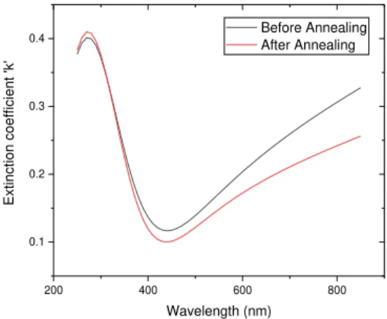
3.3 ITZO
•
30% O
2A study was also carried out to evaluate the feasibility of using ITZO instead of IGZO and ITO as TSO, as it belongs to same family of AOS. Its optical properties were also studied, as a function of wavelength before and after annealing of the samples.
200 400 600 800
1.9 2.0 2.1 2.2 Refr active ind ex ' n' Wavelength (nm) Before Annealing After Annealing
Figure 15- The variation of refractive index with wavelength, before and after
annealing, of an ITZO sample.
200 400 600 800
0.1 0.2 0.3 0.4 Extinction coe fficien t 'k' Wavelength (nm) Before Annealing After Annealing
Figure 16- The variation of extinction coefficient with wavelength, before and
after annealing, of an ITZO sample.
It can be seen in graph Figure 15 that an increase of the index of refraction is observed when the annealing is done. Although annealing improves uniformity, in this case, there is a deviation from the theoretical value of the materials that will be used as insulator [26]. On the other hand, the extinction coefficient after annealing decreases, for wavelengths above about 350 nm. As this decreasing makes the material more transparent, it is an important parameter to consider. Moreover, it can be seen from the graph of Figure 16 that the decrease is not high. This lead to the conclusion that the commitment to move away from the theoretical value of the insulators' refractive index is not justified for the stacking that will be realized in the future. Therefore, for the ITZO, importance was given to the samples before annealing. Similarly to what was done with the IGZO, the optical properties of three samples with different O2
0 5 10 15 20 25 30 1.84 1.86 1.88 1.90 1.92 1.94 1.96 1.98 2.00 2.02 2.04 2.06 2.08 2.10 2.12 Refr active ind ex ' n'
% O2
400 nm 550 nm 700 nm
Figure 17- The variation of refractive index with O2 concentration, for 3
different wavelengths, of various ITZO samples.
0 5 10 15 20 25 30
0.12 0.14 0.16 0.18 0.20 0.22 0.24 0.26 Extinction coe fficien t 'k'
% O2
400 nm 550 nm 700 nm
Figure 18- The variation of extinction coefficient with O2 concentration, for 3
different wavelengths, of various ITZO samples.
Again, for both the refractive index and the extinction coefficient, there is not a very large variation with increasing oxygen concentration is seen for the same wavelength. It can be a big advantage because, there will be several ITZO sample options with different oxygen concentrations that can be used for a certain wavelength.
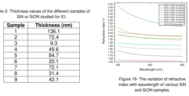
3.4 SiN and SiON
Following the study for the TSO, the study for the IO is now underway. In order to obtain SiN and SiON with different optical properties and different thicknesses first the SiH4 concentration was fixed and
the N2 and N2O concentrations were varied as shown in Table 2. In this way, nine samples were obtained
for IO, which will later be compared with the samples already studied for TSO.
Table 2- Values of the concentration of SiH4, N2 and N2O for the different samples of SiN or SiON studied for IO.
Sample SiH4 N2 N2O
1 16.8 6.3 7.0
2 16.8 13.3 5.0
3 16.8 6.3 2.0
4 16.8 6.3 5.0
5 16.8 6.3 6.0
P Table 3- Thickness values of the different samples of
SiN or SiON studied for IO.
Sample Thickness (nm)
1 136.1
2 72.4
3 9.3
4 49.6
5 84.7
6 20.1
7 72.1
8 31.4
9 42.1
400 600 800
1.60 1.65 1.70 1.75 1.80 1.85 1.90 1.95 2.00 2.05 2.10 2.15 2.20 2.25 2.30 2.35 2.40 2.45 2.50 Refr active ind ex ' n' Wavelength (nm)
SiON-1 (After Annealing) SiON-2 (After Annealing) SiON-3 (After Annealing) SiON-4 (After Annealing) SiON-5 (After Annealing) SiON-6 (After Annealing) SiON-7 (After Annealing) SiON-8 (After Annealing) SiN-9 (After Annealing)
Figure 19- The variation of refractive index with wavelength of various SiN
and SiON samples.
By analysing Table 3 in parallel with the graph of Figure 19, and excluding the samples number 2 and 9 (since they have a different concentration of N2), a trend can be observed both in relation to the
thickness and the refractive index. We can say that with increasing N2O concentration there is an increase
in thickness and a decrease in the refractive index. Regarding the two samples previously excluded, although the N2 concentration increases to 13.3, the same happens, by increasing N2O concentration
there is an increase in thickness and a decrease in the refractive index. However, despite following the trend, sample number 3 is slightly deviated from the others. This sample may be off due to extremely low thickness and oxygen concentration, leading to a fitting not correct. Once again it is concluded that the fitting is much more difficult for very thin samples, representing a detection limit of ellipsometry.
With the support of Table 2, where the concentration of SiH4 is fixed and the concentrations of N2
and N2O are varied from sample to sample, a graph was built for two different wavelengths, where the
values of these two parameters that vary can be removed, in order to obtain the desired refractive index.
7 8 9 10 11 12 13
0 1 2 3 4 5 6 7 N2 O N2 1.618 1.700 1.782 1.863 1.945 2.027 2.108 2.190 2.272 n @ 550 nm
Figure 20- The variation of the refractive index with the change in the N2 and N2O
concentrations to a wavelength of 550 nm.
7 8 9 10 11 12 13
0 1 2 3 4 5 6 7 N2 O N2 1.614 1.688 1.762 1.836 1.910 1.984 2.058 2.132 2.206 n @ 650 nm
Figure 21- The variation of the refractive index with the change in the N2 and N2O
concentrations to a wavelength of 650 nm.
As can be seen in the graphs of Figure 20 and Figure 21, the number of points that built them is limited, being therefore only the beginning to draw a full map. Thus, to be complete requires more points, that is, more samples with different N2 and N2O concentrations. In the future it will help a lot, because to
wavelength where one wants to operate, and withdraw the values of the two concentrations represented in it. However, even though it is not represented here, the extinction coefficient must also be checked so that, for the line of the required refractive index, the two graphs can be compared and then concluded which gives the lowest k.
Due to the limitations of the ellipsometry on the extinction coefficient, as mentioned above, a deeper study was carried out to verify until which value of the k can be trusted. Sample number 4 was used, i.e. a sample of SiON with 49.6 nm, and the angle of incidence of the ellipsometry was set at 75°. Subsequently, in the fitting, Tan and Cos values were withdrawn for a specific wavelength, which were then normalized. With normalized Tan and Cos values two graphs were plotted as a function of the extinction coefficient.
1E-7 1E-6 1E-5 1E-4 0.001 0.01 0.1 1 10 0.7 0.8 0.9 1.0 Ta n (k) /T an (k= 0)
Log (Extinction coefficient 'k')
Figure 22- The variation of the Tan values normalized with the extinction coefficient on a logarithmic scale.
1E-7 1E-6 1E-5 1E-4 0.001 0.01 0.1 1 10 0.8 0.9 1.0 Cos (k) /Cos (k= 0)
Log (Extinction coefficient 'k')
Figure 23- The variation of the Cos values normalized with the extinction coefficient on a logarithmic scale.
From Figure 22 and Figure 23, both for the Tan and for the Cos , there is a clear limit of the value of the extinction coefficient in which it cannot be trusted, i.e. when it is lower than 10-2. In another words, for
samples with these characteristics, for conditions where k is less than 10-2, ellipsometry cannot be used.
Nonetheless, the graphs are represented at a fixed angle of incidence of 75°, this applies for most of the high angles. It is known that there are certain thicknesses, wavelengths and angles combinations where one can go 2 orders of magnitude lower.
P
476 477 478 479 480 481
40 60 80 100 120 140 Wavelength (nm) 25 (k=0) 26 (k=0) 26.3 (k=0) 26.4 (k=0) 26.5 (k=0) 27 (k=0) 30 (k=0) 25 (k=1E-4) 26 (k=1E-4) 26.3 (k=1E-4) 26.4 (k=1E-4) 26.5 (k=1E-4) 27 (k=1E-4) 30 (k=1E-4) 25 (k=2E-4) 26 (k=2E-4) 26.3 (k=2E-4) 26.4 (k=2E-4) 26.5 (k=2E-4) 27 (k=2E-4) 30 (k=2E-4) 25 (k=0)_Measured 26 (k=0)_Measured 26.3 (k=0)_Measured 26.4 (k=0)_Measured 26.5 (k=0)_Measured 27 (k=0)_Measured 30 (k=0)_Measured
Figure 24- The variation of the values with wavelength, for angles of incidence that change between 25 ° and 30 ° and
for values of k that change between 0, 1E-4 and 2E-4.
476 477 478 479 480 481 482 -1.4 -1.2 -1.0 -0.8 -0.6 -0.4 -0.2 0.0 − (k= 0) Wavelength (nm) 25 (k=1E-4) 26 (k=1E-4) 26 (k=1E-4) 26.3 (k=1E-4) 26.4 (k=1E-4) 26.5 (k=1E-4) 27 (k=1E-4) 30 (k=1E-4) 30 (k=1E-4) 25 (k=2E-4) 26 (k=2E-4) 26 (k=2E-4) 26.3 (k=2E-4) 26.4 (k=2E-4) 26.5 (k=2E-4) 27 (k=2E-4) 30 (k=2E-4) 30 (k=2E-4)
Figure 25- The variation of the values normalized with wavelength, for angles of incidence that change between 25 ° and 30 ° and for values of k that change
between 1E-4 and 2E-4.
As can be seen in both graphs of Figure 24 and Figure 25, where a greater variation of the delta value is observed, for the different values of k, it is when the angle of incidence is equal to 27°. It can be concluded that, for samples with these characteristics, it is at this angle that the ellipsometry is more sensitive in measuring the extinction coefficient. Reason why the study to verify until which value of the k can be trusted, when measuring with this equipment, was made for an incidence angle of 27°. In the fitting, Cos values were withdrawn for a specific wavelength, which were then normalized, and with them, a graph was plotted as a function of the extinction coefficient.
1E-7 1E-6 1E-5 1E-4 1E-3 0,01 0,1 1 10 -2 -1 0 1 2 Cos (k) Cos (k= 0)
Log (Extinction coefficient 'k')
4,375E-1
Figure 26- The variation of the Cos values normalized with the extinction coefficient on a logarithmic scale.
This time, there is a clear difference in the shape of the curve, and the existence of a peak between the k values of 10-3 and 4.375×10⁻¹ in the graph of Figure 26 is notorious. For these range it is possible
coefficient, even though its value is reduced it never goes off that, as well as above 0,4375, because in this last case it changes to a metal. This is a possible reason why we don’t see any differences.
3.5 Comparison of the refractive indices
Finally, a comparative study was carried out between the candidate materials for TSO and IO. In this way, their refractive indices were analysed and then a match among them is verified. However, despite the target at the end is to have the same refractive index for both materials, it changes depending on the application. This is because the wavelength that will be used is different. Although for the video hologram project it is interesting to do this study for the entire spectrum, especially for the wavelengths 450 nm, 550 nm and 650 nm, which correspond to blue, green and red, respectively. Initially it was given more importance to the green region because it is the one that is used for optical devices.
Initially, the correspondence between the IGZO and the SiN or SiON was analysed, through its refractive indices as a function of the wavelength.
400 600 800
1.8 2.0 2.2 Refr active ind ex ' n' Wavelength (nm)
0% O2 (After Annealing) 6% O2 (X1) (After Annealing) 6% O2 (X2) (After Annealing) 10% O2 (MO1) (After Annealing) 10% O2 (MO2) (After Annealing) 50% O2 (5P) (After Annealing) 50% O2 (10P_1) (After Annealing) 50% O2 (10P_2) (After Annealing) SiON-4 (After Annealing) SiON-5 (After Annealing) SiON-6 (After Annealing) SiON-7 (After Annealing) SiON-8 (After Annealing) SiN-9 (After Annealing)
550
Figure 27- The comparison of the refractive index of IGZO and SiN or SiON samples as a function of wavelength.
The first aspect that can be concluded from the graph of Figure 27,that it will be difficult to find two candidates that will work for the entire spectrum. This is because of having refractive index curves with different slopes for both materials However, as can be seen, it is already possible to find some matches for certain wavelengths, especially for 550 nm. As discussed above, by changing the concentration of SiH4, N2 and N2O in the deposition of SiN or SiON, it is possible to change its refractive index in order to
approach the one from IGZO. So, depending on the wavelength where it is desired to work, it will be possible to obtain and choose an IO that fits perfectly with the IGZO.
P Figure 28- The comparison of the refractive index of ITZO and SiN or SiON samples as a function of
wavelength.
In this case, by the evaluation of the graph of Figure 28, it is concluded that there are 4 curves which should be given more relevance. Those are ITZO samples with 10% and 30% of O2, and those of
samples number 4 and number 9 of SiON and SiN, respectively. As it is possible to observe, between the wavelength range of interest, that is, between 450 nm and 650 nm, all have a similar slope, which means that they have refractive indices very close to each other. For the future, a better alignment of the dispersion of ITZO and SiN or SiON can be achieved by an adjustment of the concentrations of SiH4, N2
and N2O. Still, it has to be mentioned that the curve of the ITZO with 0% O2, is showing a deviation from
the expected Cauchy type dispersion from approximately 550 nm in comparison to the other two ITZO samples. Here, more time has to be spent on a correct modelling of the optical constants in future developments.
Finally, the same comparative study was also performed for ITO. Therefore, the correspondence between this material and SiN or SiON was analysed through its refractive indices as a function of wavelength.
400 600 800
1.8 2.0 2.2 550 Refr active ind ex ' n' Wavelength (nm)
6% O2 - 50 nm (After Annealing) 6% O2 - 70 nm (After Annealing) 6% O2 - 80 nm (After Annealing) 6% O2 - 30 nm (After Annealing) SiON-4 (After Annealing) SiON-5 (After Annealing) SiON-6 (After Annealing) SiON-7 (After Annealing) SiON-8 (After Annealing) SiN-9 (After Annealing)
Figure 29- The comparison of the refractive index of ITO and SiN or SiON samples as a function of wavelength.
Similarly to what was stated above for the ITZO sample with 0% of O2, the same happened to the
4 ITO samples. The fitting for this material, which despite being one of the simplest and most common, was quite difficult, leading to the conclusion that for this it would be necessary to create a new law that would allow a more precise and reliable fitting. Due to reason that the model is not the most correct, the curves go downwards and present a slope quite different from what was expected. Because of this large difference in the slopes of the refractive index curves of the two materials, it is possible to obtain some combinations between ITO and SiN or SiON, but only for a specific wavelength. In order to obtain a greater
400 600 800
1,8 2,0 2,2 Refr active ind ex ' n' Wavelength (nm)
Conclusion and Future Perspectives
In the previous chapters, we have noticed that the main challenge is to find a new metamaterial without a different. refractive index. It has been demonstrated that this challenge is not only related to the material conductor and the insulating oxides but also to process variables that can be changed in their depositions.We identified that SiN and SiON are promising candidates, because we can easily tune the refractive index, by changing the parameters, in particular the gas concentration of the reactors in the ICP-CVD process. Therefore, they can be combined with different conductors.
Three different conductors, IGZO, ITO and ITZO, were screened. Despite the target composition changes from conductor to conductor, the rest of the process is the same for all three. This means that, although it is not possible to deposit the three conductors at the same time, no special preparation is required for any of them, which is a great advantage in the deposition process. Also, from the results obtained, it can be concluded that for all of them, combinations with SiN or SiON were found, where they have an identical refractive index for a specific range of wavelengths. Meaning that we are not limited, for example, to the ITO for being the "standard" TCO. However, so far, IGZO is the preferred candidate in combination with SiN or SiON. Because although it is already possible to find several matches for certain wavelengths, especially for 550 nm, the wavelength used for optical devices, it is the conductor that presents a slope of the curve of the index of refraction more similar to the one of the insulating oxides.
In the future, other conductor candidates can be used and subsequently only adjust the SiN or SiON properties. That is, it is a very flexible system.
For the moment, it is a challenge to extend the spectral range of refractive index overlap to broadband conditions. In future material combinations, the slopes of the complex refractive index of insulator and conductor should be identical.
On the other hand, the determination of the extinction coefficient is still challenge. For the application being studied, a low k is required, which cannot be detected when using ellipsometry. Thus, there is an urgent need to find other methods to measure the k.
Still related to ellipsometry, there is also a need to perceive, for each material, the best measurement parameters to determine k. Because by measuring with a certain angle its value is different from measuring with another. That is, for each material or stack of layers with different materials, it is necessary to make a previous study to conclude the best option as angle of incidence to put in the ellipsometry.
References
[1] D. Gabor, Nobel Lecture. 1971.[2] H. J. Eichler and A. Hermerschmidt, “Light-Induced Dynamic Gratings and Photorefraction,” in
Photorefractive Materials and Their Applications 1, 2006, pp. 7–42.
[3] C. M. Soukoulis and M. Wegener, “Past achievements and future challenges in the development
of three-dimensional photonic metamaterials,” Nat. Photonics, vol. 5, 2011.
[4] K. Nomura, H. Ohta, A. Takagi, T. Kamiya, M. Hirano, and H. Hosono, “Room-temperature
fabrication of transparent flexible thin-film transistors using amorphous oxide semiconductors,”
Nature, vol. 432, pp. 488–492, 2004.
[5] G. P. Gonçalves, “Filmes finos de óxido de índio e zinco e sua aplicação em díodos orgânicos
emissores de luz,” Universidade Nova de Lisboa, 2011.
[6] E. B. Aydın and M. K. Sezgintürk, “Indium Tin Oxide (ITO): A promising material in biosensing
technology,” TrAC Trends Anal. Chem., vol. 97, pp. 309–315, 2017.
[7] A. Vlooswijk, “Growth & Characterization of p-type Transparent Oxide Semiconductors,”
Universidade de Twente, 2005.
[8] D. M. Mattox and V. H. Mattox, Review of Transparent Conductive Oxides (TCO). 2007.
[9] M. Z. H. Khan, “Effect of ITO surface properties on SAM modification: A review toward biosensor
application,” Cogent Eng., vol. 3, 2016.
[10] C. A. Hoel, T. O. Mason, J.-F. Gaillard, and K. R. Poeppelmeier, “Transparent Conducting Oxides in the ZnO-In 2 O 3 -SnO 2 System,” Chem. Mater., vol. 22, no. 12, pp. 3569–3579, 2010.
[11] R. Upadhyay, “Integration and Characterization of High Mobility Oxide Semiconductor Into Thin-Film-Transistor,” Amity University, 2017.
[12] K. Yim et al., “Computational discovery of p-type transparent oxide semiconductors using hydrogen
descriptor,” npj Comput. Mater., vol. 4, no. 17, 2018.
[13] T. Kamiya, K. Nomura, and H. Hosono, “Present status of amorphous In-Ga-Zn-O thin-film
transistors,” Sci. Technol. Adv. Mater., vol. 11, 2010.
[14] T. Kamiya, K. Nomura, and H. Hosono, “Origins of High Mobility and Low Operation Voltage of Amorphous Oxide TFTs: Electronic Structure, Electron Transport, Defects and Doping*,” J. Disp.
Technol., vol. 5, no. 7, pp. 273–288, 2009.
[15] N. Martin, T. Nyberg, and V. Kapaklis, “Low temperature electronic transport in sputter deposited
a-IGZO films,” Curr. Appl. Phys., vol. 14, no. 11, pp. 1481–1485, 2014.
[16] M. J. Gadre and T. L. Alford, “Highest transmittance and high-mobility amorphous indium gallium zinc oxide films on flexible substrate by room-temperature deposition and post-deposition anneals,”
Appl. Phys. Lett., vol. 99, 2011.
[17] T. Gupta, “Dielectric Materials,” in Copper Interconnect Technology, 2009, pp. 67–110.
[18] J. A. Appels, E. Kooi, M. M. Paffen, J. J. H. Schatorjé, and W. H. C. G. Verkuylen, “Local Oxidation of Silicon and Its Application in Semiconductor-Device Technology,” Philips Res. reports, vol. 25,
pp. 118–132, 1970.
[19] F. I. Riley, “Silicon Nitride and Related Materials,” J. Am. Ceram. Soc., vol. 83, no. 2, pp. 245–265,
2000.
P
Appendix
•
Complete study for an ellipsometry fitting (in this case for a SION sample)
SEA regression report summary
Details
Software and regression log
Software about Semilab - Spectroscopic Ellipsometry Analyzer - SEA Software version 1.5.1
Officially licensed to IMEC
Operator fonsec27
Date and time of regression 18-05-2018 15:47 Comments
Layer structure
Overview
Optical model
Phase 2 Dispersionlaws
Dispersion law Cauchy
Thick Dispersionlaws
Dispersion law Cauchy
D31_Corrected_Measure
P
Regression results
Measurement information
Measurement file path Z:\UserData\Ellipsometer\SiON (05-2018)\After Annealing\75\ D31_Corrected_Measure.mse
Angle of Incidence 68°
Regression details
Regression 1 (EllipsoReflectance)
Wavelength range 400 - 850 nm Angle of Incidence 68°
Fit to Tan(Ψ), Cos(Δ)
Angular Aperture 3°
Fit algorithm LMA
Results
Parameters Value Fitted 2 σ confidence limit Unit Model
AOI Shift 0 °
Angular Aperture 3 °
Phase 2 (Dispersionlaws)
Thickness 57.929 X 0.00195 nm
B (μm^2) -0.10312 X 0.03167 μm^2
C (μm^4) 0.01674 X 0.00393 μm^4
D 0
E (μm^2) 0 μm^2
F (μm^4) 0 μm^4
N_inf 2.06169 X 0.05789
Thick (Dispersionlaws)
Thickness 0 nm
B (μm^2) 0.00178 μm^2
C (μm^4) 0.00012 μm^4
D 0
E (μm^2) 0 μm^2
F (μm^4) 0 μm^4
N_inf 1.5107
Derived parameters Value Phase 2 (Dispersionlaws)
n @ 632.8 nm 1.9086
k @ 632.8 nm 0
Thick (Dispersionlaws)
n @ 632.8 nm 1.5159
k @ 632.8 nm 0
Ambient (void)
n @ 632.8 nm 1
k @ 632.8 nm 0
Fit quality
R^2 0.85839
P
P
Correlation coefficients
Ph2 - Dispersionlaws
- Thickness Ph2 - Cauchy - B (μm^2) Ph2 - Cauchy - C (μm^4) Ph2 - N_inf
Ph2 - Dispersionlaws
- Thickness 1 0.0567 0.0043 -0.1375 Ph2 - Cauchy - B
(μm^2) 1 -0.9889 -0.9622
Ph2 - Cauchy - C
(μm^4) 1 0.9132


![Figure 4- Schematic setup of the DC Sputtering deposition process. Adapted from [22].](https://thumb-eu.123doks.com/thumbv2/123dok_br/16692646.743703/28.893.153.819.322.537/figure-schematic-setup-dc-sputtering-deposition-process-adapted.webp)