41 PACS numbers: 68.55 aj, 73.90 + F
EFFECT OF SUBSTRATE TEMPERATURE ON STRUCTURAL AND MORPHOLOGICAL PARAMETERS OF ZnTe THIN FILMS
K.D. Patel1, G.K. Solanki1, C.J. Panchal2, K.S. Hingarajiya1, J.R. Gandhi1
1 Department of Physics, Sardar Patel University
Vallabh Vidyanagar, 388 120, Gujarat, India E-mail: [email protected]
2 Faculty of Technology, Applied Physics Department,
M.S. University of Baroda, Vadodara 390001, Gujarat, India
Vacuum evaporated thin films of Zinc Telluride (ZnTe) of 5000 thickness have been deposited on glass substrates at different substrate temperatures (303 K, 373 K, 448 K). Structural parameters were obtained using XRD analysis. Atomic Force Microscope (AFM) in non-contact mode has been used to study the surface morphological properties of the deposited thin films. The results obtained from structural and surface morphological studies have been correlated and it is found that the films deposited at higher substrate temperatures possess increasingly good crystallinity and smoother surfaces.
Keywords: ZNTE THIN FILM, THERMAL EVAPORATION, XRD, AFM, SUB-STRATE TEMPERATURE.
(Received 04 February 2011, in final form 17 March 2011)
1. INTRODUCTION
Thin films of II-VI compound semiconductors have drawn researcher’s attention for more than four decades. ZnTe is expected to be a promising material for a variety of optoelectronic devices, such as pure green light emitting devices, detectors for various optoelectronic instrumentation, etc. because of its direct wide band gap of 2.26 eV [1-3]. It is also used as terahertz detectors [4, 5] and window material for CdTe based solar cells [6]. Many researchers have used various techniques for the fabrication of ZnTe thin films including Metal organic chemical vapor deposition [7], MBE [8], vacuum evaporation [9-11] R.F. Sputtering [12] and Electrodeposition [13-17]. Among these, thermal evaporation technique offers several advantages including simplicity and cost effectiveness for larger area processing. In this paper we report our results of our investigations on structural and morphological properties dependence on substrate temperature in case of ZnTe thin films deposited using thermal evaporation technique.
2. EXPERIMENTAL
Thin films of ZnTe were deposited on an ultrasonically cleaned glass substrates using thermal evaporation technique, under a vacuum of 10 – 6 Torr at different substrate temperatures (303 K, 373 K and 448 K). A
CuK radiation and the surface morphological study was carried out using atomic force microscope in non-contact mode with tungsten carbide tip.
3. RESULTS AND DISCUSSION
3.1 Structural Analysis
The X-ray diffractograms of the thin films deposited at various substrate temperatures are shown in Fig. 1. It is observed that XRD patterns of all three films show a most preferred orientation along (111) plane. Also the most prominent peak is observed nearly at 25.6 for 2 , which shows that the deposited films possess cubic structure [18]. Structural parameters of the deposited films are given in Table 1. The sharper and intense peaks, in Fig. 1, for films deposited at increased substrate temperatures exhibit an improved crystalline structure of the films. Particle size values also increases with increase in the substrate temperature.
0 5000 10000 15000 20000 25000 30000 35000 40000 45000 50000 55000 60000 65000 70000
20 25 30 35
L
in
(
C
o
u
n
ts
)
Ts = 448 K Ts = 373 K Ts = 303 K
2
0 5000 10000 15000 20000 25000 30000 35000 40000 45000 50000 55000 60000 65000 70000
20 25 30 35
L
in
(
C
o
u
n
ts
)
Ts = 448 K Ts = 373 K Ts = 303 K
2
Fig. 1 – XRD peaks of ZnTe thin films of thickness 5000 , deposited at various substrate temperatures
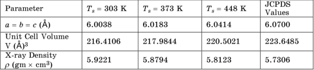
Table 1 – Structural parameters of ZnTe thin films of thickness 5000
deposited at various substrate temperatures
Parameter Ts 303 K Ts 373 K Ts 448 K JCPDS Values
a b c ( ) 6.0038 6.0183 6.0414 6.0700
Unit Cell Volume
V ( )3 216.4106 217.9844 220.5021 223.6485
X-ray Density
(gm cm3) 5.9221 5.8794 5.8123 5.7306
3.2 Morphological Analysis
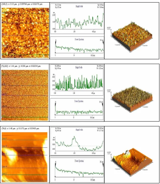
Fig. 2 – Two and three dimensional images of ZnTe Thin films of Thickness 5000 , deposited at various substrate temperatures: Ts 303 K (a), Ts 373 K (b), Ts 448 K (c)
a b c
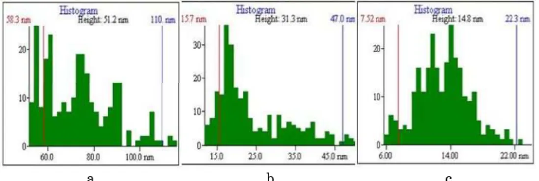
Fig. 3 – Histograms of ZnTe thin films of thickness 5000 , deposited at various substrate temperatures: Ts 303 K (a), Ts 373 K (b), Ts 448 K (c)
Table 2 – Data obtained from AFM analysis of ZnTe thin films
A difference between peak and valley values (RP-V), obtained from the height profile is listed in Table 2. A large difference in the value of RP-V for all five lines of the image of film at lower substrate temperature (ranging from 44.15 nm to 210.7 nm) shows a poor surface smoothness of that film. The films deposited at higher substrate temperature show relatively low value of RP-V. Thus it is again confirmed by the difference of peak and valley observations made along five arbitrarily scanned horizontal lines of AFM scan that as substrate temperature increases, the surface smoothness improves. -7.454 10.98 10.41 14.65 5.025 13.20 13.13 2.585 3.271 18.44 448 -12.25 26.94 17.10 27.71 5.930 20.25 24.00 7.600 9.161 39.18 373 -21.17 42.88 59.20 78.49 5.150 72.91 73.09 11.97 14.81 64.05 303 05 -7.913 9.676 10.36 14.85 5.039 13.15 13.06 2.540 3.151 17.59 448 -18.79 30.09 15.04 28.69 5.935 22.44 24.01 8.404 10.27 48.89 373 -20.94 223.21 61.87 80.12 5.156 73.15 73.11 9.193 10.74 44.15 303 04 -4.665 6.495 11.12 14.27 5.020 12.82 13.12 1.909 2.387 11.16 448 -19.00 26.73 13.59 29.36 5.997 22.93 23.98 8.846 10.61 45.73 373 -59.92 150.8 19.04 113.9 5.150 30.45 73.14 61.26 68.35 210.7 303 03 -6.366 14.62 9.77 14.01 5.032 12.07 13.10 3.126 4.201 20.99 448 -17.69 26.34 14.19 29.23 6.101 23.29 23.99 8.474 10.31 44.03 373 -42.43 164.4 37.48 73.21 5.076 47.43 73.12 39.21 53.39 206.8 303 02 -6.891 9.970 10.13 15.04 5.032 12.92 13.14 2.865 3.482 16.86 448 -17.31 32.66 13.59 28.51 6.069 21.48 23.99 9.558 11.52 49.98 373 -14.79 109.9 61.27 71.21 5.049 66.61 73.15 12.87 24.72 124.7 303 01 Valley RV (nm)
Peak RP ( nm)
Bearing Ratio @80% (nm) Bearing Ratio @30% (nm) Arc Lth (µm) Med. Ht (nm) Mean Ht. (nm) RAVG (nm) RRMS (nm)
RP-V
(nm) Sub. Tem. (k) Line -7.454 10.98 10.41 14.65 5.025 13.20 13.13 2.585 3.271 18.44 448 -12.25 26.94 17.10 27.71 5.930 20.25 24.00 7.600 9.161 39.18 373 -21.17 42.88 59.20 78.49 5.150 72.91 73.09 11.97 14.81 64.05 303 05 -7.913 9.676 10.36 14.85 5.039 13.15 13.06 2.540 3.151 17.59 448 -18.79 30.09 15.04 28.69 5.935 22.44 24.01 8.404 10.27 48.89 373 -20.94 223.21 61.87 80.12 5.156 73.15 73.11 9.193 10.74 44.15 303 04 -4.665 6.495 11.12 14.27 5.020 12.82 13.12 1.909 2.387 11.16 448 -19.00 26.73 13.59 29.36 5.997 22.93 23.98 8.846 10.61 45.73 373 -59.92 150.8 19.04 113.9 5.150 30.45 73.14 61.26 68.35 210.7 303 03 -6.366 14.62 9.77 14.01 5.032 12.07 13.10 3.126 4.201 20.99 448 -17.69 26.34 14.19 29.23 6.101 23.29 23.99 8.474 10.31 44.03 373 -42.43 164.4 37.48 73.21 5.076 47.43 73.12 39.21 53.39 206.8 303 02 -6.891 9.970 10.13 15.04 5.032 12.92 13.14 2.865 3.482 16.86 448 -17.31 32.66 13.59 28.51 6.069 21.48 23.99 9.558 11.52 49.98 373 -14.79 109.9 61.27 71.21 5.049 66.61 73.15 12.87 24.72 124.7 303 01 Valley RV (nm)
Peak RP ( nm)
Bearing Ratio @80% (nm) Bearing Ratio @30% (nm) Arc Lth (µm) Med. Ht (nm) Mean Ht. (nm) RAVG (nm) RRMS (nm)
RP-V
(nm)
Bearing ratio is the two dimensional projection of three dimensional surface. It gives a percentage of covered area in a film at the particular height. Thus it shows a length of the particle above a horizontal line throughout the distribution. Bearing ratio allows a comparison of roughness data for all three films and it is listed in Table 2. There is a large difference in these values (ranging from 71.21 nm to 113.9 nm @ 30%) and 19.04 nm to 61.87 nm @ 80 %) for the film deposited at Ts 303 K. For other two
films with Ts 373 K and 448 K these differences are comparably smaller.
Power spectrum curve is the important parameter in analysis of any rough surface. It determines the contact area between two solids and can provide both, lateral and longitudinal information. A convenient way to describe surface roughness is to represent it in the term of profile heights
z(x, y). For a typical digitized AFM scans, the value of x and y are quantized. Thus the power spectra exhibit the overall surface features of the deposited films as shown in Fig. 2. Looking to all three curves it is clear that the curve for the film at Ts 303 K possess an irregular and spread
peaks in comparison to that of the other two films. Peaks in the power spectrum indicate the periodicity of the surface and frequency of each peak gives a length that defines this periodic surface. Spread peak exhibits the deviations from average value. The spectrum for the film at Ts 373 K
exhibits a sharp peak showing better surface properties.
Mean height, which is the central value of the roughness profile over the evaluation length, decreases as the substrate temperature of the deposited film is increased, showing a better smoothness of the film surface. The median height which is a mid point on the roughness profile over the evaluation length such that half of the data fall above it and half below it, is also inversely proportional to the substrate temperature of the film. In the obtained data, there is a large variations in median value for the film at
Ts 303 K, particularly at line number 2 and 3, which can also be seen from
the Fig. 3. The large difference in mean and median values of the film deposited at Ts 303 K shows an asymmetric distribution.
The histogram is a continuous bar diagram in which, each column represents the number of image pixels having the height value in a particular range. The histograms for the deposited films are shown in Fig. 2. It indicates a decrease in height from 51.2 nm to 14.8 nm for the films deposited at Ts 303 K to 448 K.
4. CONCLUSION
The authors are thankful to Department of Chemistry, Sardar Patel University, Vallabh Vidyanagar and SICART, Vallabh Vidyanagar for AFM characterization and XRD analysis.
REFERENCES
1. D. Kurbatov, V. Kosyak, M. Kolesnyk, A. Opanasyuk and S. Danilchenko,
Integrated Electronics 103, 32 (2008).
2. R. Bhargava, Properties of wide band gap II-VI semiconsuctors- London, United Kingdom: INSPEC, The Institution of Electrical Engineers, 238 (1997).
3. T. Tanaka, K. Saito, M. Nishio, Q. Guo and H. Ogawa, J. Mater. Sci. Mater. Electron. 20, 505 (2008).
4. T. Ishizaki, N. Saito, O. Takai, S. Asakuru, K. Goto and A. Fuwa, Electrochim. Acta 50, 3509 (2005).
5. C. Winnewisser, P.U. Japsen, M. Schall, V. Schiyja. H. Helm, Appl. Phys. Lett. 70, 3069 (1997).
6. P.V.S. Meyers, Proceedings of seventh Commission European Communities Confrrence o Photovolatic Solar Energy, Redial, Dordrecht, 1121, (1986)
7. K. Wolf, H. Stanzl, A. Naumov, H.P. Wagnor, W. Kuhn, B. Kahn, W. Gebhardt,
J. Cryst. Growth 138, 412 (1994).
8. R.L. Gunshor, L.A. Kolodziejski, N. Otsuka, S. Datta, Surf. Sci. 174, 522 (1986). 9. U. Pal, S. Saha, A. K. Chaudhari, V.V. Rao, H.D. Benarji, J. Phys. D: Appl. Phys.
22, 965 (1989).
10.R. Sarma, N. Mazumdar and H.L. Das, Bull. Mater. Sci. 29, 11 (2006).
11.G.I. Rusu, P. Prepilita, N. Apetroaei and G. Popa, J. Optoelectron. Adv. M. 7(2), 829 (2005).
12.H. Belakhder, A. Outzourhit, E.L. Ameziane, Thin Solid Films 382, 30 (2001). 13.M. Neumann-Spallart, C. Konigstein, Thin Solid Films 265, 33 (1995).
14.A.B. Kashyout, A.S. Arico, P.L. Antonucci, F.A. Mohamed, V. Antonucci,
Mater. Chem. Phys. 51, 130 (1997).
15.K.K. Mishra, K. Rajeshwar, J. Electroanal. Chem. 273, 169 (1989). 16.M.C. Lin, P.Y. Chen, I.W. Sun, J. Electrochem. Society 149, 653 (2001).
17.B. Bozzini, M.A. Baker, P.L. Cavallotti, E. Cerri, C. Lenardi, Thin Solid Films 388, 361 (2000).