Effect of Annealing on the Properties of Nanocrystalline CdS Thin Films Prepared by CBD Method
A. Djelloul1,2,*, M. Adnane1, Y. Larbah1, M. Zerdali1, C. Zegadi1, A. Messaoud2
1Department of Material Technology, Physics Faculty, USTOMB University, BP1505 Oran, Algeria 2Centre de Recherche en Technologie des Semi-Conducteurs pour l’Energétique ‘CRTSE’ 02 Bd Frantz Fanon,
BP 140, 7 Merveilles, Alger, Algérie
(Received 26 January 2016; published online 21 June 2016)
The CdS thin films were deposited on glass substrate by chemical bath deposition (CBD). The effect of annealing temperature on the morphological, structural, optical and electrical properties of the crystalline CdS films were investigated for different annealing temperature (as deposited, 300, 400 and 500 °C).The annealing time is 1 h. The materials have been prepared using simple aqueous solutions containing cad-mium sulfate, as source of cadcad-mium, and thiourea as source of sulfur and ammonium hydroxide as the complexing agent. The temperature of the bath was maintained at low temperature of 80 °C. The surface morphological properties studied by SEM and AFM respectively. The structural properties of CdS thin film was studied by X-ray diffraction. The optical parameter such as transmittance and energy band gap of the films with thermal annealing temperature was investigated by UV-Visible spectrophotometer. The varia-tion of band gap values of CdS thin film samples were found to be in the range of 2.37 to 2.5 eV. Electrical resistivity measurements were carried out in four-probe Van Der Pauw geometry at room temperature by the Hall measurement. SEM image confirmed that film of smooth surface morphology.
Keywords: CdS, Glass substrate, CBD, Annealing temperature, Energy band gap.
DOI: 10.21272/jnep.8(2).02005 PACS numbers: 81.05. 81.05.Kf. 81.10.Dn. 78.66.Hf
1. INTRODUCTION
Cadmium sulfide (CdS) is a wide band gap semicon-ductor, which is used as an efficient window material for the fabrication of superstrate type solar cell struc-ture due to its low resistivity and high transmitivity [1-3]. It has been used as a window layer in high effi-ciency thin film solar cells base on cadmium telluride (CdTe), copper indium diselenide / sulphide (CIS) and copper indium gallium diselenide / sulphide (CIGS) [4]. It has been used in the deposition of CdS semiconduc-tor thin films since the 1960s [5, 6] and many tech-niques including electrodeposition [7, 8], spray pyroly-sis [9], successive ionic layer adsorption and reaction (SILAR) [10], vacuum evaporation [11], and Chemical Bath Deposition (CDB) [12-14]. CBD is known to be a simple method, with low temperature and inexpensive large area deposition technique, it use an aqueous solu-tion and then we can control the chemical parameters of solution like (temperature, molar concentration, PH, time of deposition, stirring rate., etc.) [15, 16]. There-fore we can control the thickness of the film and grain size of the particle then the energy band gap. The CdS deposition by chemical bath deposition (CBD) is based on the controlled precipitation of metallic ions (Cd2+) in a solution containing sulfide ions (S2-) of controllable concentrations. This can be achieved by two mecha-nisms [17]:
a) Ion by ion (heterogeneous reaction); b) Cluster by cluster (homogeneous reaction).
The formation process of CdS nanoparticles are proposed as follows [18]:
The cationic precursor solution releases Cd2+ ions from [Cd (tartaric acid)]2+ as:
[Cd(tartaric acid)]2+ → Cd2+ + tartaric acid (1)
NH3 + H2O ↔ NH4+ + OH– (2)
In the anionic precursor solution, thiourea hydroly-sis occurs and gives S2– ions according to:
CS(NH2)2 + OH–↔ CH2N2 + SH– + H2O (3)
SH– + OH–↔ S2– + H2O (4)
Finally the CdS are formed by combinaison of Cd2+ with S2– ions as:
Cd2+ + S2–↔ CdS (5)
In this work, CdS thin films were prepared by CBD at temperature 80 °C. The effect of the annealing in air atmosphere at 300, 400, 500 °C are discussed. The X-ray diffraction (XRD), fourier transform infrared (FTIR), secondary ion mass spectrometry (SIMS), scanning electron microscopy (SEM), atomic force microscopy (AFM), photoluminescence (PL), UV-Visible spectrosco-py and four-probe Van Der Pauw method by the Hall measurements are used to characterize the CdS thin films.
2. EXPERIMENTAL DETAILS
2.1 Sample Preparation
the pH value about 10.
Films were deposited on glass substrates (Micro slides Glass) thickness (1.35 mm) and size (75 25 mm), these substrates were emerged in ultra-sonic bath (in different solution such as ethanol, ace-tone) for 30 minutes and finally washed by distilled water, in order to clean them.
The bath was covered. Then under continuous stir-ring dustir-ring the deposition to ensure homogeneous dis-tribution of the chemicals, the clean glass slide were vertically immersed in the beaker contain the solution which was placed in chemical bath solution. Deposition time was 60 min, during which the solution color changed to yellow. After deposition, the CdS films were removed from the bath and washed with water ultra-sonically to remove the loosely adhered CdS particles on the film and finally dried in air. The obtained films are homogeneous, densely packed and smooth well adherent to the glass substrate. All the films used in the present investigation were deposited simultaneous-ly from the same bath deposited using the same chemi-cal solution at different annealed with a fix tempera-ture. Fig. 1 shows the schematic diagram of the exper-imental method.
Fig. 1 – Schematic diagram of Chemical Bath Deposition
3. CHARACTERIZATIONS
The surface morphology of the nanostructure films was investigated with scanning electron microscope (SEM) (JEOL, (JSM-6610LA)) and atomic force micros-copy (AFM-JSPM 5200). The structural characterization of the films was analyzed using X-ray diffractometer
(XRD) (Siemens D500) with Cu Kα radiation. The Four i-er Transform Infrared (FTIR) spectra of the samples were recorded using JASCO FT-IR 460 spectrometer by KBr pellet technique in the range 400-4000 cm– 1. The secondary ion mass spectrometry (SIMS) measurements were carried out by means of a Cameca IMS 4F-E7 mass spectrometer using a 10 kV Cs+ primary ion beam with an incidence angle around 32 with respect to the surface normal . The sheet resistance (Rs) of the samples was measured using a four-point technique and the
Resistiv-ity measurements were carried out in Four-Probe Van Der Pauw geometry at room temperature by the Hall measurements (HL5900). The optical transmittance measurements of the films were performed with a UV-Visible spectrophotometer (Cary 500).
4. RESULTS AND DISCUSSION
4.1 Scanning Electron Microscopy (SEM)
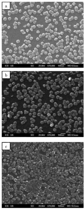
In order to study the microstructures of CdS thin films prepared by CBD method, scanning electron mi-croscopy (SEM) was used. Fig. 2 shows the SEM images of as-deposited and annealed (at 300, 400 and 500 °C) thin films. In Fig. 2(a) spherical shaped nanoparticles with vacant spaces were observed, while on annealing, the film consists of dense layer of small crystallites and the nanoparticles convert into bigger clusters due to the coalescence or diffusion of large number of CdS nanoparticles which can be seen in Fig. 2(b), (c) and (d).
b
а
Fig. 2 – SEM images of CdS thin films: (a) – as-deposited; (b)-(d) – annealed (at 300, 400 and 500 °C)
The distribution of nanoparticles becomes more ordered and the vacant spaces between them get occupied. This can be explained as during the annealing, the recrystal-lization process densified the film and eliminated the defects in the material.
4.2 Atomic Force Microscopy (AFM)
Fig. 3 (a) and Fig. 3 (b) show the three-dimensional and two-dimensional atomic force microscopy (AFM) images for cadmium sulphide (CdS) thin films after annealing at 400 °C deposited on glass substrate respe c-tively. The AFM image was measured for an area of 5.00 5.00 um 140.0 nm. The substrate surface is well covered with grains and spherical shaped nanoparticles
Fig. 3 – 2D and 3D AFM images of CdS thin film after anneal-ing at 400 °C
that are uniformly distributed over the whole surface. The average sizes of smaller grains are observed to be 80 nm and the surface is relatively uniform because the nanoparticles convert into bigger clusters due to the coalescence or diffusion of large number of CdS nanopar-ticles (see SEM images). The average surface roughness and thickness is 45.50 and 65 nm respectively.
4.3 X-Ray Diffract (XRD)
Fig. 4 illustrates the XRD spectra for the as-deposited and annealed thin CdS films at 400 °C. The pulses (in arbitrary unit) and diffraction angle (2θ) were plotted. The spectra of CdS films are compared with ASTM cards of CdS structure, and indicated a crystalline structure of cubic phase (JCPDS -042-1411). This result is in agreement with Kozhevnikova et al [18]. Fig. 4(a) shows the X-ray diffraction pattern of the as-grown CdS thin film. The broad lump in the range of
scanning angle of 10° to 70° is due to the amorphous
glass substrate.
Fig. 4– X-ray diffraction data of the CdS thin films: (a) – as-deposited; (b) – annealed at 400 °C
However after annealing at 400 °C, the XRD pa t-terns revealed that the films have cubic phase with a preferred orientation in the (111) plane (see Fig. 4(b)).This improvement may be attributed to re-crystallization of the films structure, by the enhance-ment of the rearrangeenhance-ment of Cd and S atoms in the film crystallites after. The grain size of CdS film an-d
a
b
nealed at 400 °C was evaluated to be between 10.5 nm to 13.8 nm by using the Debye Scherrer’s formula [19].
cos k
D
(6)
D is the crystallite diameter;
is the wavelength of the incident radiation ( 0.152 nm);
the width at half height of the diffraction peak; θ the half-angle Bragg diffraction expressed in radi-ans.
4.4 Fourier Transform Infrared (FTIR)
Abstract is an essential part of the article metadata. The Fourier transform infrared (FTIR) measurements were undertaken to confirm the formation of the CdS thin films. Fig. 5 show the FTIR spectrum in the frequency range (450-4000 cm– 1) of CdS thin film after annealing at 400 °C. It can be seen that the sample shows a weak characteristic vibrations of cadmium sulfide located at 635.54 cm– 1, others peaks are attributed to the formation of CdS nanoparticles.
Fig. 5– FTIR spectrum of CdS thin film after annealing at 400 °C
4.5 Secondary Ion Mass Spectrometry (SIMS)
The SIMS profile of CdS thin films are shown in Fig. 6. The apparently high signal of 28Si, 114Cd, 16O and 1H and 32S in the CdS film is due to the relative sensitivity factor (RSF) which, begins to decrease with depth. The presence of 114Cd and 32S in SIMS profiles with a high signal at the interface can be ascribed to the possible formation of cadmium sulphide (CdS); this result confirms the presence of Cd-S band observed on the FTIR spectra.
4.6 Optical Transmissions
An important tool for searching and structuring of scientific and technical information is the keywords that are pointed in the article.
The optical properties of the films deposited on glass substrates were determined from the transmis-sion and reflection measurements in the range 200-1100 nm.
Fig. 6 – SIMS profile of CdS thin films elaborated by chemical bath deposition (CBD)
Fig. 7 shows the transmission spectra of as deposit-ed and annealdeposit-ed CdS films. The annealing tempera-tures were 300, 400, 500 °C with one-hour annealing time; after each step the optical transmittance of the sample was registered and next annealing was made with the same sample. The results show that the opti-cal transmission is more than 75 % in the visible range for as deposited and annealed films.
The changes of transmittances are associated to the increase measured over the visible range.
Fig. 7 – Transmittance spectra of CdS thins films: (a) – as-deposited; (b)-(d) – annealed (at 300, 400 and 500 °C)
The band gap energy (Eg) of the films is derived by using the relation [20, 21]:
2
g
h K h E
where K is a constant and Eg is the band gap energy. The absorption coefficient () which is a function of the photon energy (hν) is calculated from the optical transmittance spectra results using the following equa-tion [22]:
ln Td
(8)
Where d is the thickness of the film and T is the op-tical transmittance. The (Eg) value is determined by extrapolating the linear part of the plot (hν)2 versus (hν) in the abscissa (X axis), which indicates a direct optical transition. The (hν)2 versus (hν) plots for both as-prepared and annealed CdS films are shown in Fig. 8 and the determined bang gap values are listed in Table 1. The annealed samples show a relative de-crease in band gap with annealing temperature. These results are consistent with other published results such as results of George, et al. [23] who attribute this de-crease in the band gap in the annealed samples to the grain size growth and composition changes taking place in the samples by CdO identified by XRD. Whereas Nair, et al. [24] reported that the temperature-dependent parameters that affect the band gap are reorganization of the film, sulfur evaporation and self-oxidation of the film. The reorganization of the film should occur at all annealing temperatures. By filling the voids in the film one expects denser films and lower energy gaps. It is a known fact that some of the sulfur leaves the film at temperatures higher than 375 C.
Table 1 – Effect of annealing on optical band gap of the CdS films deposited on glass substrates
№
Ech
Annealing Tempera-tures
Optical Band gap (eV)
1 As-Deposited 2.5
2 300 °C 2.42
3 400 °C 2.48
4 500 °C 2.37
The decrease in band gap after annealing can be at-tributed to improvement in the crystallinity with anneal-ing temperature as supported by XRD studies. Similar effect has been observed for CBD grown CdS films [25]. It was clear that the band gap is decreased due to an in-crease of the cluster size or grain size and this is known as the quantum size effect. This can be explained as during the annealing, the recrystallization process densified the film and eliminated the defects in the material.
Fig. 8 –Transmittance spectra The band gap of nanocrystalline CdS thin films under different annealed-temperatures: (a) – as-deposited; (b)-(d) – annealed (at 300, 400 and 500 °C)
5. PHOTOLUMINESCENCE (PL)
CBD allows the growth of small grained CdS films at low temperatures, at 80 °C. Fig. 9 shows the PL spectra at 10 K for the samples studied in this work. In this figure, it can be seen that there are different PL bands for CBD-CdS layers before and after annealing at 400 °C. Later, we have confirmed these results by XRD. PL measurements reveal the existence band for CBD-CdS films grown on glass substrates. This band decreases in intensity with annealing temperature at 400 °C.
5.1 Electrical Properties
Content of the main part should be logically related, set out clearly, prepared in scientific style, and have a corresponding structure.
a
b
c
Fig. 9 – PL spectra of CdS thin films: (a) – as-deposited; (b) – annealed at 400 °C
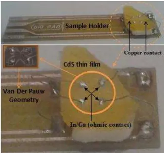
The electrical properties of the CdS films are exam-ined at room temperature by resistivity and Hall measurements using Van der Pauw method (see Fig. 10) and summarized in Table 2. CdS exhibits n-type conductivity. The nature of the charge carriers were measured by hot probe method and confirmed by Hall measurement.
Electrical Profiles were performed by using a Accent HL5900 Hall system. The sample holder of the Hall profile machine is shown in figure 10 with In/Ga eutectic was used for ohmic contact (see Fig. 10). The current of
1 mA was applied through the sample and a magnetic field of 0.32 T was applied. The results are presented in Table 2. The films exhibit very low resistivity found to be 3.23 10– 4Ωcm and the mobility attains 194 cm2/Vs. The sample owns a sheet resistance equals to 58.6 Ω/□, a high electrical conductivity found to be 0.31 104 S/cm and an average Hall coefficient around 1.14 cm2/C.
Fig. 10 – CdS films mounted onto sample holder
Table 2 – The electrical properties of CdS thin films after annealing at 400 °C
№
Ech Sample
Sheet
re-sistance (Ω/□) Conductivity type
Hall coefficient (m2/C)
Resistivity
(Ω.cm) Mobility (cm2/Vs)
3 Annealed at 400 °C 58.6 N – 1.14 3.23 10–
4 194
6. CONCLUSION
In this paper, we used a simple and easily-controllable method to elaborate CdS nanoparticles thus a good quality, adherent and uniform for different annealing temperature (300, 400 and 500 °C).
Structural, surface morphological, optical and elec-trical properties of the CdS films fabricated by a simpli-fied CBD technique using cadmium sulfate and thiou-rea precursors have been studied in detail. The struc-tural studies revealed that the films have cubic phase with a preferred orientation in the (111) plane after annealing at 400 °C temperature.
In our experiment, based on the optical transmis-sion measurements, the band gap energies are calcu-lated to be between 2.37-2.5 eV for the CdS films with different annealing temperature (as deposited, 300, 400 and 500 °C). The result promises a potential applic a-tion of chemical bath deposited CdS thin films for the solar cells. Morphology and optical properties of the CdS films were characterized using SEM, AFM, UV-Visible spectroscopy and PL spectra.
The films have a cubic structure with optical transmission is more than 75 % in the visible range for
as deposited and annealed films. Annealing slightly improves the crystallinity and reduces the optical bandgap with increase in annealing temperature. This new route for CBD gives dense, compact and uniform CdS thin film after annealing of the films. The best annealing temperature for CBD grown CdS films was found to be 400 °C from the optical and morphological properties. CdS shows n-type conductivity. Its resistivi-ty is about 3.23 10– 4 Ω.cm and the mobility attains 194 cm2/Vs. CdS exhibits characteristics compatible with window material for solar cells.
ACKNOWLEDGMENTS
This work was supported by the all member of La-boratory of Electronic Microscopy and Materials Sci-ence in University of SciSci-ence and Technology of Oran
‘USTO’ and Centre de Recherche en Technologie des
REFERENCES
1. K.P. Chopra, S.R. Das, Thin Films Solar Cells, New York, 424 (1979).
2. K.W. Mitchell, C. Eberspecher, J. Enmer, D. Pier, Proc, 20th IEEE, Photovoltaîc Spi, Conf, IEEE, Isc, 1384 (1989). 3. L.Q. Pham, T.K. Van, H.G. Cha, Y.S. Kang, Cryst. Eng.
Commun. 14, 7888 (2012).
4. M.A. Contreras, M.J. Romero, B. To, F. Hasoon, R. Noufi, S. Ward, K. Ramanathan, Thin Solid Films 403, 204
(2002).
5. I. Oladeji, L. Chow, C. Ferekides, V. Viswanathan, Z. Zhao, Sol. Energ. Mater. Sol. C. 61, 203 (2000).
6. M.F. Bertino, R.R. Gadipalli, J.G. Story, C.G. Williams, G. Zhang, C. Sotiriou-Leventis, A.T. Tokuhiro, S. Guha, N. Leventis, Appl. Phys. Lett. 85, 6007 (2004).
7. J. Zhang, L. Sun, S. Liao, C. Yan, Solid State Commun.
124, 45 (2002).
8. B.M. Basol, E.S. Tseng, D.S. Lo, US Patent 4, 681 (1984). 9. S.J. Castillo, A. Mendoza-Galvan, R. Ramirez-Bon,
F.J. Espinoza Beltran, M. Sotelo-Lerma, J. Gonzalez-Hernandez, G. Martinez, Thin Solid Films373, 10 (2000). 10.B.R. Sankapal, R.S. Mane, C.D. Lokhande, Mater. Res.
Bull. 35, 177 (2000).
11.U. Pal, R. Silva-Gonzalez, G. Martinez-Montes, M. Gracia-Jimenez, M.A. Vidal, S. Torres, Thin Solid Films305, 345
(1997).
12.F. Ouachtari, J. Mod. Phys. 2, 1073 (2011).
13.R. Zahid, Z. Azmi, M.G. Mohd Sabri, J. Atefeh, U.D. Fasih, Z. Reza, Int. J. Mol. Sci. 12, 1293 (2011).
14.J. Han, C. Spanheimer, G. Haindl, G. Fu, V. Krishnakumar, J. Schaffner, C. Fan, K. Zhao, A. Klein, W. Jaegermann, Mater. Res. Bull.46, 194 (2011).
15.D. Saikia, P.K. Gogoi, P.K. Saikia, Chalcogenide Lett. 7, 317 (2010).
16.H. Khallaf, I.O. Oladeji, G. Chai, L. Chow, Thin Solid
Films516, 7306 (2008).
17.N.S. Kozhevnikova, A.S. Vorokh, A.A. Uritskaya, Russ.
Chem. Rev. 84, 225 (2015).
18.Y.A. Kalandagh, M.B. Muradov, R.K. Mamedov, M. Behboudnia, A. Khodayari, Optoelectron. Adv. Mater.-Rapid Commun. 2, 42 (2008).
19.S.Z. Lahewil Abdulwahab, Y. Al-Douri, U. Hashim, N.M. Ahmed, Sol. Energ.86, 3234 (2012).
20.B. Subramanian, C. Sanjeevviraja, M. Jayachandran,
J. Crystal Growth234, 421 (2002).
21.A.V. Feitosa, M.A.R. Miranda, J.M. Sasaki, M.A. Araújo -Silva, Brazilian J. Phys.34, 2B (2004).
22.Y.P. Venkata Subbaiah, P. Prathap, K.T. Ramakrishna Reddy, Appl. Surf. Sci.253, 2409 (2006).
23.P.J. George, A. Sanchez, P.K. Nair, M.T.S. Nair, Appl.
Phys. Lett. 66, 3624 (1995).
24.P.K. Nair, G.O. Daza, R.A. Arias-Carbajal, J. Campos, M.T.S. Nair, Semicond. Sci. Technol. 16, 651 (2001). 25.G. Bakiyaraj, N. Gopalakrishnan, R. Dhanasekaran,