Paulo Henrique de Godoy
pegodoy@uol.com.br
Emílio Carlos Nelli Silva
Member, ABCM ecnsilva@usp.br Escola Politecnica, University of Sao Paulo Dept. of Mechatronics and Mechanical Syst. Eng. 05508-900 São Paulo, SP. Brazil
Aspects of Fabrication and
Characterization of Electro-Thermal
Micro-Actuators
This study examines the behavior of well known simple thermal micro-actuators. This work describes some unexplored aspects of the employed methodology to produce these electro-thermal micro-actuators (ETMs). These information could be time saving for new groups to start research and development on electro-thermal actuators. The focus of the applied methodology is the use of the finite element method (FEM) applied to an iterative procedure to predict the behavior of the micro-actuators before production. The computational model is adjusted based on measurements of force and displacement. To be correctly applied, this methodology requires a sensitivity study of the material properties. The results emphasize the need to use FEM with more accurate thermal and mechanical properties, and to consider also the variation of these properties with temperature. We must also consider a careful definition of thermal boundary conditions and the effects of heat convection and radiation, due to deviations between experimental results and FE results. In this investigation, the structural material applied was Nickel, plated at about 1 µm/min. The experimental characterization was carried out in a micro probe station with a CCD (charge-coupled device) camera attached to it, and used a controlled voltage source.
Keywords: MEMS, micro-actuators, force measurement, displacement measurement, FE simulation
Introduction
Micro-electromechanical Systems (MEMS in EUA) or Microsystems Technology (MST in Europe and Asia) covers mechanical micro-components (mobile or not) whose dimensions can range from hundreds of microns to a few millimeters. Such micro-systems can be integrated with the microelectronic circuitry (such as accelerometers and pressure sensors) or not (such as valves and inkjet heads) [Petersen 1982, Rai-Choudhury 2000, Ishihara et al. 1996].
1
This research focuses on the study of micro-actuators whose main purpose is to produce an action in the system in which they are located. There are various ways in which to actuate these microstructures. The first three of the following ways to drive a micro-actuator are the most common: capacitive or electrostatic, piezoelectric, electro-thermo-mechanic, magnetic, or shape memory alloys (SMA). Actuating the microstructure electro-thermo-mechanically has advantages such as linearity between applied voltage-obtained displacement, and higher force (compared to a capacitive drive), however a longer response time when compared to the other two most usual forms of actuation (capacity and piezoelectric). [Rai-Choudhury 2000, Ishihara et al. 1996; Jonsmann 1999; Mankame et.al. 2001; Que et.al. 2001]. Another benefit is that no special or "exotic" material is needed to perform the actuation, making the production comparatively easy. Electro-thermo-mechanical micro-actuators (or simply ETM micro-actuators) work on the basic principle that the thermal expansion of their elastic structure will produce displacement. This thermal energy is supplied to the system by the electrical resistance when an electric current flows through the structure (Joule effect). If the microstructure is properly anchored to a substrate, the thermal energy lost through the substrate is minimized, remaining in the micro-device and contributing to maximize the generation of mechanical strain and so displacement. The applications that combine great demand for in-plane force with minimal chip-area are the most promising of the many possibilities of the ETM micro-actuators usage (such as micro-positioning, micro-gripping, micro-switching, force generation) [Sinclair 2000].
Paper accepted October, 2006. Technical Editor: José Roberto de F. Arruda.
The fabrication of these microstructures requires costly materials and is time consuming. The common process is based on a trial-and-error system. It takes a long time to be performed with no guarantee of satisfactory results. Due to such difficulties, the development of new micro-systems clearly needs to be performed using an integrated approach (design-fabrication-characterization). In addition, this integrated approach can minimize the number of required prototypes, thus lowering costs. Therefore, an iterative procedure was applied which consists of five steps: (i) design, (ii) computational simulation (predicting its initial behavior), (iii) physical implementation (fabrication), (iv) characterization, and (v) re-evaluation of the computer model based on real properties. The study of these aspects contributes to improve the methodology for the development of these MEMS. Normally these aspects are not clearly presented on publication and their understanding can demand some effort.
This article is organized as follows. Section 3 includes a complete description of each phase of the process, including the problems encountered, and the solutions adopted. Section 4 discusses a sensitivity study using FEM including material properties in the performance of electro-thermal micro-actuators. Section 5 reevaluates the computational model to make it relevant to the current case. After that, the analysis is ready for predicting future designs. Section 6 presents some conclusions about the results, and Section 7 is the bibliography.
Nomenclature
[M] = Structural mass matrix; [C] = Structural damping matrix; [Ct] = thermal specific heat matrix;
[K] = Structural stiffness matrix; [Kt] = thermal conductivity matrix;
[Ktb] = thermal conductivity matrix of material;
[Ktc] = thermal conductivity matrix of convection surface;
[Kv] = electric coefficient matrix;
{Fnd] = applied nodal force vector;
{Fth} = thermal strain force vector;
{Fpr} = pressure load vector;
{Qnd} = applied nodal heat flow vector;
{Qg} = heat generation rate vector due to causes other than
Joule heating;
{Qj} = heat generation rate vector due to Joule heating; {Ind} = applied nodal electric current vector;
{u} = displacement vector;
{T} = thermal potential (temperature) vector; {V} = electric potential vector;
Superscripts. . time derivative . . second time derivative
Development Procedure of Electro-Thermal Micromechanisms
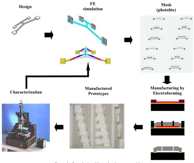
The whole process of design and fabrication can be summarized in Figure 1. The process consists of seven steps: (i) The micro-actuator is designed using computer aided design (CAD) tools; (ii) Finite element analysis is performed to predict the micro-actuator initial behavior (based on previously studied properties); (iii) the mask lay-out is carried out using the most cost effective technique - photolite; (iv) Electroplating (copper, nickel, some alloys) of the microstructures onto substrates such as alumina or silicon wafer (copper, nickel, some alloys); (v) wet stripping of sacrificial layers is applied to finish the prototypes; (vi) experimental characterization of displacement, blocking force, and electrical resistance; (vii) re-evaluation of the computational model based on experimental data.
Figure 1. The overall process for electro-thermal microstructures development.
Designing the Micro-Actuators
These micro-actuators can be designed by using two distinct approaches: (i) a systematic methodology, called topology optimization, and (ii) a trial and error method, the so-called "intuitive" design.
The traditional trial and error method requires continual design, fabrication, and characterization of the microstructures until the
satisfactory result can be obtained (with optimal shape). This process is very time consuming, however it does use simple geometric shapes.
Topology optimization distributes the material in an initial and fixed design domain, reduced to finite elements in order to maximize cost effectiveness [Bendsøe 1995]. This concept reduces the time to achieve the optimal shape. However, topology optimization generates complex shapes [Sigmund 2000]. Since this paper describes a systematic approach for the development of
Mask (photolite)
Characterization
Design FE
simulation
Manufacturing by Electroforming Manufactured
Prototypes
these structures focusing on the influence of the performance of material properties, we have chosen to consider the micro-actuators with a so-called ‘simple design’, made of a union of simple shapes, based on some well-established concepts [Que et.al. 1999; Park et.al. 2000; Chu et.al. 2003].
Figure 2 shows a micro-actuator with an opened-"V" geometry (defined by θ) with two possible design conditions: with or without a spring. The structural angle θ is given by Que et al. [Que et.al. 1999] so that the maximum displacement is obtained. These micro-actuators have a line width of 50 microns, and the anchor pads are squares of 250 microns. In Figure 2c, there is a spring attached to the micro-actuator whose function is to allow us to measure the force data by indirectly measuring its displacement. The spring behavior (stiffness) was designed by FE analysis to block the micro-actuator displacement at maximum workload. The observed displacement of the spring results in a blocking force that stops the micro-actuator movement.
(c)
Figure 2. ETM micro-actuators with unidirectional movements: (a b) without spring (c) with attached spring.
Modeling the Microstructures by the Finite Element Method (FEM)
The FE analysis of micro-actuators was carried out using the ANSYS software, which has specific elements for MEMS simulation, such as the element SOLID 98. In this analysis, the correct definition of the boundary conditions and material properties are very important for the final result.
In the modeling implementation, the input parameters are the specified nodal temperature and nodal voltage, specified surface forces (natural convection), and physical material properties. The Eq. (1) shown below is solved for displacement, current density, and temperature gradient.
[ ] [ ] [ ]
[ ] [ ] [ ]
[ ] [ ] [ ]
[ ] [ ] [ ]
[ ]
[ ]
[ ]
[ ] [ ]
[ ]
[ ] [ ] [ ]
[ ]
[ ]
[ ]
[ ] [ ]
[ ]
+ + + V T u K K K V T u C C V T u M v t t 0 0 0 0 0 0 0 0 0 0 0 0 0 0 0 0 0 0 0 0 0 & & & & & & & & & & & & (1) where:[Kt] = [Ktb] + [Ktc]
{Q} = {Qnd} + {Qc} + {Qg} + {Qj} {I} = {Ind}
{F} = {Fnd}+{Fth}+{Fpr}
The FE analysis in ANSYS can be carried out either with coupled or uncoupled (multi-physics) fields. There are three aspects to take into account when choosing between them. The first is the ease of usage. On coupled-field analysis the insertion of the boundary conditions is carried out just once and all the results come out together. In multi-physics simulations, each phenomenon is modeled separately (with its own boundary conditions), and the input data for the next phenomenon being the solution of the previous one. This could take too much time to implement without software experience. A second aspect is the disk usage and the time to solve the problem. In a coupled-field analysis, the three environments are solved simultaneously, which demands long computational time. On the other hand, in multi-physics analysis the amount of disk usage and time to solve it are considerably smaller because each phenomenon (electrical-thermal-mechanical) is solved separately. Finally, there is the possibility to include non-linear effects for displacement that may occur at high power inputs [Sigmund 2000]. In multi-physical phenomenon, a non-linear feature for displacement can be considered with the structural element SOLID92, which is not available in the coupled-field element SOLID98. If this feature must be modeled, then multi-physics environment must be chosen. Both elements have tetragonal shape and are appropriate for irregular meshes.
Considering the boundary conditions, the correct values of the voltage and the thermal boundary conditions are important because they can affect the final result considerably. The voltage must be applied to the central node of the mechanical anchor (electrical pad). There are two ways to apply the thermal boundary conditions as shown in Figure 3: (i) imposing the environmental temperature directly at the bottom of the mechanical anchors (called "essential thermal boundary condition" or ETBC); or (ii) imposing the environmental temperature at the substrate (called "natural thermal boundary condition" or NTBC). The NTBC must be used in structures whose thermal dissipation is not ideal at substrate. This condition increases the overall energetic efficiency of the micro-actuator [Mankame et.al., 2001] and leads to a more accurate result for displacement/current. However, it does have a higher solution time because the substrate must also be simulated. In this work, the ETBC condition was used to reduce the solution time.
(a) (b)
Figure 3. Models for thermal boundary conditions definition: (a) NTBC; (b) ETBC.
The material properties together with thermal boundary conditions are the most important factors that affect the simulation results. Table 1 summarizes the properties used for the initial modeling of the structures (structural material Nickel). Young´s modulus and thermal expansion coefficient were obtained from Jonsmann [Jonsmann 1999], and all other properties came from the Material’s Handbook by [Lide 1998].
θ
l
θ
l
Spring length - l
Movement direction
(b)
Table 1. Nickel Material properties.
E* 188 GPa
Υ 0.31
α* 15 ppm/K
Density 8908 g/cm3
T Kx T ρ
(K) (W/mK) (K) (µΩ.cm)
250 97.5 273 6.16
300 90.7 293 6.93
350 85 298 7.12
400 80.2 300 7.20
500 72.2 400 11.8
600 65.6 500 17.7
800 67.9 600 25.5
1000 71.8 700 32.1
1200 76.2 800 35.5
1400 80.4 900 38.6
The Fabrication Technique
The fabrication technique used here [Madou 1997] combines ultra violet lithography (UV-lithography), electroplating of copper and nickel and selective etching. The UV-lithography consists of patterning a photopolymer layer with UV light in order to form a mold. Lithographic masks delimit the area of the mold. Normally, the size of the minimal aspects defines the type of lithographic mask. Masks with minimal aspect of 1 to 10 microns necessarily have a high production cost (such as e-beam). In the case of this work, the chosen type of lithographic mask was the one that has a line resolution of 30-40 microns. Although it has a low cost, it also has the poorest quality. The mask has many pores and a line roughness factor – rugosity - of 2 to 3 microns, although these problems do not restrict its usage on the project.
Usually, most MEMS groups make use of microelectronics to produce such Microsystems. This consists of expensive lithographic masks, silicon as substrate, and the use of sophisticated equipment [see Geiger et.al. 2002; Rai-Choudhury 2000]. In this study, the micro-actuators were fabricated by electroplating. Figure 4 shows a schematic diagram of the apparatus used in the process. This apparatus for metal plating consists of a 2000 ml glass Beaker placed over a hot plate, a constant current source, an amp meter, a stirrer, a metallic anode, and a sample holder. The applied structural material was Nickel [Jonsmann 1999]. Since the structures are supposed to be mobile, a sacrificial layer must be produced. The easy strip of the sacrificial layer is an important variable to take into account when choosing the sacrificial material layer. The material used as a sacrificial layer in this case was Copper because of its selective-stripping to Nickel. Other options could exist for the sacrificial material layer such as the use of photo resists. However, in that case, the mask quality must be good enough and the post-cure parameters (temperature-time) appropriate to prevent blister formation. The electrolytic solutions have their compositions described in Table 2. To complete the electrolytic solution, additives (chemical substances) can also be used to improve some aspects of the deposits such as: grain size, uniform thickness, level of internal stress, and metal brilliance. Additives such as saccharin, boric acid, a commercial brilliance improver, a commercial leveler, and a commercial wetter were used. However, these additives can also modify the mechanical, electrical and thermal properties of the deposits, and the use of organic substances on the electrolytic solutions mainly lead to the formation of pits. These defects consist of cavities on the structures due to lack of metal. To avoid this, it is necessary to use the appropriate amount of organic additives, to apply degreaser to the sample prior to electroforming, avoid touching it with bare hands and to control the hydrogen evolution at cathode (sample). This can be avoided by simply applying cathodic
or anodic movement, bubbling oxygen at sample, or with less effect, stirring the electrolytic solution. This last procedure is the simplest to use, and thus, it is the method used in this study.
Figure 4. Schematic drawing of the electroplating apparatus.
Table 2. Electrolyte Composition.
Nickel bath
Nickel sulphate (22%), g 300 Nickel chloride, g 60
Boric acid, g 45
DWK Brilliance improver, ml 7.5
DWK Leveler, ml 35
DWK Wetter, ml 21
Copper Bath
Copper sulphate, g 75 Sulfuric acid, ml 100 Chloridric acid P.A., ml 0.15 PCM additive, mL 5
Figure 5 describes the production process employed. The substrate consists of an alumina plate of two square inches. Two layers of metals were applied onto the substrate to form the seed-layer. The seed-layer is necessary because alumina is not conductive. The conductive layer is made by 0.2 microns of sputtered gold. To improve the adhesion of gold to alumina, a titanium layer with 0.02 microns thickness was sputtered first [Johanssen 2000]. Table 3 shows all the processes, time, and employed reactants. The first step consists of patterning the sacrificial layer mold since the thickness of the copper layer is about 6-12 microns. AZ-4620 (Clariant) was chosen as a photo resist. This photo resist is easy to strip (just acetone) and to manipulate. To improve AZ adhesion to the substrate it is a common task to spread an adhesion promoter like HMDS (Hexa Methyl Di Silazane). After the processing of the AZ mould, the copper layer was plated at a solution temperature of 25ºC. After checking the film thickness, the AZ mould is stripped with acetone and the substrate cleaned.
Since the structural layer usually takes more than 50 microns, SU-8 100 (Shipley) was chosen as the negative type photo-resist as a second layer, this mask must be aligned with the previous one through alignment marks. Figure 6 presents the two alignment marks used in the project. The first mark leaves at the substrate a square ring of copper. The second mark is a “plus” and fits inside the copper square ring. Usually, the patterns do not have a uniform width, shape or size. This factor is important because the molds are not filled at the same rate. Thin lines are filled faster than wide ones.
A
Hot plate with magnetic stirring NiP or copper
electrode
Magnetic stir
Beaker
Amp meter
Therefore, thin areas must be checked during the electroplating process instead of large ones.
Sacrificial Layer
Mold: AZ-4620 Seed-layer
Substrate Structural layer
Mold SU-8
Free-standing structure
Figure 5. Process sequence.
When the nickel film was finished, the SU-8 mold was removed, the sample was cleaned and all the thicknesses re-checked. After that, the sample was ready for copper, gold, and titanium stripping. Copper is selectively stripped from nickel by a mixture of hydrogen peroxide, ammoniac, and de-ionized water, 1:1:3. Usually, the whole sample can be completely free after an hour or two. Gold is etched by a KCN-based etchant and titanium is etched by flouridic acid. Finally the microstructures are ready for usage.
Table 3. Processing time for positive and negative photo resists.
AZ4620 (positive)
Layer thickness 14 microns
Spinning 4000rpm 27s HMDS
bake 95ºC 10 min
Spinning 1000rpm 27s Photoresist
bake 40-95ºC (~3º/min) 13min UV exposition 9.5 W 160 s
Developing AK-400 1:3 120 s
Final bake 5min 95 ºC
SU-8 100 (negative) Layer thickness 70-80 microns
Layer spinning 4000 rpm 27 s
Bake 5/15/5 min 65/95/65 ºC
UV exposition 11 W 23 s
Pos-bake 5/15/5 min 65/95/65 ºC Developer 180 s
Figure 6. Marks used to align the copper layer (AZ mould to the left) with nickel layer (SU-8 mould to the right).
The micro-actuators produced can be seen in Fig.7. There were three types: micro-actuators with free-displacement to obtain the displacement; and another type with two types of springs (1200 microns and 600 microns). The micro-actuators with the smaller spring presented smaller displacements, so the larger spring was used for force measurement.
(a)
(b)
(c)
Figure 7. Fabricated micro-actuators: (a) blocked by a 1200 µm spring; (b) blocked by a 600 µm spring; and (c) for free-displacement.
250 µm 250 µm
The Characterization Step
The characterization of the microstructures is focused on two variables: force and displacement. The force data was obtained indirectly by measuring the displacement of a spring (see Fig. 2). The displacement of the free-actuator and spring-actuator set is obtained indirectly by calibrating pictures taken before and after actuation. In the absence of a more reliable methodology (such as micro metrology), this method fits our needs.
To characterize the micro-actuator, firstly it was necessary to determine how the electric power would be applied to the system. There are two possibilities for electrical power control: (i) control by voltage, and (ii) control by current. If control by current is employed, a point of electrical instability can take place [Ashcroft 1991; Jonsmann 1999], mainly because of the interdependency between electrical resistivity and temperature. Thus, the electrical power was controlled by voltage.
The experimental characterization consists of applying voltage to the micro-actuator obtaining the current data, and finally capturing an image of the micro-actuator after movement (if there was any). The voltage application began at 50 mV, later to 100mV, and kept going from 100 to 100 mV until 1.7 V. Once we obtained the voltage and current data, the resistance of the employed metal can be calculated.
Results and Discussion
The calibration of the computer model is a complicated task because the material has different behaviors (properties) at a macro- and micro-level [Jonsmann 1999]. This can be noted in the sensitivity tests carried out to analyze the influence of certain material properties in computer model. The material properties investigated were the heat convection coefficient (and its boundary conditions), electrical resistance, elastic modulus, thermal conductivity, and thermal expansion coefficient. This systematic approach consisted of specifying different material tables to the FE model and observing the final result of electrical current, displacement, and body temperature. The applied voltage and structural thickness were kept constant at 1.4 volts and 28 microns, respectively.
The values assumed for the heat convection coefficient are 0, 5000, 18700, 33000, 55000 W/m2K. The experimental derivation of these values is involved, but the value of 18700 W/m2K was obtained experimentally with some simplification [Jonsmann 1999] and the value 55000 W/m2K was calculated by [Sigmund 2000]. The other values were used to observe the influence in that range. It was observed that this variable has a strong influence on displacement and body temperature (1492% and 995% respectively) rather than on electrical current (–24% respectively). The mechanism of displacement is based on Joule heating of the structure. The smaller the heat convection coefficient is, the more the structure will move (the Joule heat is concentrated on the structure). This effect has less influence on electrical current with a reversal behavior. For the next analysis, the heat convection
coefficient h was kept constant and equal to 18700 W/m2K
[Jonsmann 1999].
The Young´s modulus has insignificant influence on structure behavior in the range of ± 30% of the base value (1.8 GPa). For the coefficient of expansion, three values were considered: 15 ppm/K [Josmann 1999]; 13.4 ppm/K [Lide 1998]; and 16.6 ppm/K (obtained from the percentual variation between the first two). The displacement, body temperature, and electrical current were evaluated again. The body temperature and electrical current had no significant deviation (less than 0.1%). The displacement obtained with the experimental value is 11% higher than the displacement
obtained with tabled values indicating that this property is another variable that must be carefully observed in the computer model.
The thermal conductivity coefficient has a complex dependence upon the temperature, different from the three previous properties. To simplify the analysis of the thermal conductivity coefficient, two other tables were constructed from tabled properties by simply varying ±15% from their values. Based on this assumption, the coefficient has negligible influence in structural displacement and temperature (1.08% and 1.33%, respectively).
Finally the electrical resistivity property, showed the most important influence in structural behavior, because it can significantly affect the displacement and the electrical current over a temperature range of 400K. The model tables were constructed similarly to the tables of thermal conductivity coefficient (with a variation of ±30% from the standard table, however). The influence detected was: 11% and 30% for displacement; 7% and 22% for body temperature; and 15% to 28% for electrical current.
Thus, this study verified that some properties have more influence on micro-actuator behavior (such as heat convection coefficient, thermal expansion coefficient, and electrical resistance) than others (such as the Young´s modulus and the thermal conductivity coefficient).
Characterization
There are differences in material properties between the micro- and macro-worlds. One of the major differences is electrical resistance, which clearly imposes some interference on micro-structure behavior thus making it necessary to calibrate this property before use on computer models. Its quantification and a deeper analysis will be investigated in future work. However, it is sufficient to say that there is an interesting difference between electrical resistance on solution with and without additives, assigning the solution with additives the higher value. Because of this, the electrical resistance (and possibly other properties) cannot be used directly without verifying that the electroplating conditions (deposition parameters and plating solution) are analogous. For the purposes of this work, the value for electrical resistivity used was the one obtained from the parameters described in table 2 for bath composition.
Figure 8 demonstrates the experimental data for displacement. Figure 8(a) shows the quadratic dependence of the displacement on electrical current. Figure 8(b) presents the correlation of the displacement in relation to applied voltage. As can be seen, the initial voltage is almost linear with respect to displacement. The non-linear displacement starts over 900 mV.
(a)
(b)
Figure 8. (Continue).
Temperature is an important variable during actuator driving. A high temperature mainly leads to oxide formation (oxidation) on an actuator surface, thus, modifying its behavior. This variable is difficult to measure because any kind of sensor interferes with the behavior of the thermal actuator (such as altering the heat of convection). In the case of this investigation, the maximum work temperature was limited to 610K by choosing the correct voltage during the FE (ANSYS) simulation.
The blocking force was determined indirectly by calculations on the obtained displacement of the spring attached to the micro-actuator. The displacement obtained over the actuator-spring set is smaller than the displacement obtained on the free-actuator. This is important to ensure that the maximum force is obtained. The result is plotted in Fig. 9.
Figure 9. Force measurement.
To start a simple comparison between the actuation in other substrates, the same structures were produced on silicon, which conducts the generated heat faster than alumina. The micro- actuators of silicon and alumina substrates had different thicknesses. To compare the displacement between the two a ratio between the resulting displacement and thickness (named Figure of Merit) was considered. The displacement obtained on the alumina substrate is higher than that obtained on the silicon substrate. This fact is probably related to a lesser loss of heat from the microstructure to the substrate, improving the energetic efficiency of the micro-actuator.
Figure of Merit
thickness nt displaceme =
Γ (2)
Figure 10. Comparison of the experimental displacement between silicon and alumina substrate.
Re-Evaluating the Computational Model
The complete cycle for the micro-actuator implementation requires a feedback of the experimental data to the computational model in order to make the computational model more realistic, reducing the time for a micro-actuator final release. In this case, the initial computational model used material properties obtained from the literature. However, the plated material strongly influences the electroplating and additives employed. The first results showed a large difference between the experimental and the computational displacements. The measurement of the resistance of the Nickel plated starts to converge with the experimental data.
There are two important aspects in comparing the relevant models: the electrical current and the displacement. The computational and experimental data obtained for the electrical current points to no more than 3% of deviation. However, the data for displacement points to larger deviations between the two curves. The computational model must still be improved, because there may be more variables as of yet unexamined. Among these variables, thermal conductivity and the thermal expansion coefficient could be inducing some unevaluated influence on the thermal distribution in the micro-actuator causing a variation of the displacement value.
Figure 11. Comparison between experimental data and modeling results for displacement and current.
Supplied Power
Fi
gu
re
o
f M
Figure 11. Comparison between experimental data and modeling results for displacement and current.
Conclusion
The development of metallic MEMS actuators necessarily covers a couple of systematic phases. The basis for this paper is that to minimize the use of costly materials, the number of prototypes and the overall development time, an iterative procedure can be applied as an alternative to the trial-and-error approach. This design process consists of using computational tools to predict the micro-actuator behavior prior to its construction. However, the application of this methodology requires the proper use of materials, properties, and boundary conditions. The most relevant properties were mapped by a sensitivity study based on the computational model. Among material properties that are important for the computational model are: electrical resistance, the thermal convection coefficient, and the thermal expansion coefficient. These properties are very dependent on production processes and cannot be used directly from literature unless the process is similar. Normally these properties need to be analyzed separately to obtain suitable values for the relevant construction process. This computational model can be more accurate and more studies will be carried out to improve it.
As a future work, a more systematic study on electrical resistivity, thermal convection coefficient, and thermal expansion coefficient need to be carried out to improve the correlations between temperature and infrared imaging or another kind of non-contact temperature sensor.
Acknowledgments
The work reported in this paper is carried out in the framework of a post-doc research program conducted by the first author. We
gratefully acknowledge the financial support of FAPESP (Fundação de Amparo à Pesquisa do Estado de São Paulo). We also acknowledge Brazilian Synchrotron Light Laboratory (LNLS) for access to the facilities and all the Laboratory of Microfabrication (MIC) Staff for the technical assistance. In particular, we thank Mr. Angelo Gobbi and Ms. Maria Helena for their invaluable help.
Bibliography
Ashcroft, M., 1991, Solid State Physics, Saunders College Int. Ed. Bendsøe, M.P., 1995, “Optimization of Structural Topology, Shape, and Material”, Springer, Berlin.
Chu, L.L., and Gianchandani, Y.B., 2003, “A micromachined 2D positioner with electro-thermal actuation and sub-nanometer capacitive sensing”; J. Micromech. Microeng. No.13 pp.279–285.
Geiger, W., Butt, W.U., Gaiber, A., Frech, J., Braxmaier, M., Link, T., Kohne, A., Nommensen, P., Sandmaier, H., Kang, W., and Sandmaier, H., 2002, “Decoupled microgyros and the design principle DAVED”; Sensors and Actuators A Vol.95, pp.239-249.
Ishihara,H., Arai,F., and Fukuda,T., 1996, “Micro Mechatronics and Micro-Actuators”, IEEE/ASME Transactions on Mechatronics, Vol. 1, No. 1, pp. 68-79.
Johansen, L.S., 2000, “Microelectronics for micromechanics”, PhD thesis, The Microelectronics Centre, Technical University of Denmark, Denmark, 236 p.
Jonsmann,J., 1999, “Technology development for topology optimized thermal micro-actuators”, PhD thesis, The Microelectronics Centre, Technical University of Denmark, Denmark, 116 p.
Lide, D.R., 1998, “CRC Handbook of Chemistry and Physics”, Publisher: CRC Press. 79th edition. 2496 p. ISBN: 0849304792.
Madou, M. J., 1997, “Fundamentals of Microfabrication”, CRC Press, EUA.
Mankame, N.D., and Ananthasuresh, G.K., 2001, “Comprehensive thermal modeling and characterization of an electro-thermal-compliant micro-actuator”; J. Micromech. MicroEng. Vol.11, pp.452-462.
Park, J-S., Chu, L.L., Siwapornsathain, E., and Gianchandani, Y.B., 2000, “Long throw and rotary output electro-thermal actuators based on bent-beam suspensions”; IEEE International Microelectromechanical Systems Conference, Japan, pp. 680-685.
Petersen,K., 1982, “Silicon as mechanical material”, Proc. IEEE Electron. Devices, Vol.70, No.5, pp.420-457.
Que, L., Park, J.-S., and Gianchandani, Y.B., 2001, “Bent-Beam Electrothermal Actuators—Part I: Single Beam and Cascaded Devices”, Journal of Microelectromechanical Systems, Vol.10, No.2, 247-254.
Que, L., Park, J-S., Gianchandani, Y.B., 1999, “Bent-Beam Electro-Thermal Actuators for High Force Applications”, IEEE International Microelectromechanical Systems Conference, Orlando, FL, pp. 31-36.
Rai-Choudhury, P., 2000, “MEMS and MOEMS technology and applications”, Ed. by SPIE-Press, 520 p., ISBN 0-8194-3716-6.
Sinclair, M.J., 2000, “A high force low area MEMS thermal actuator”, In IEEE Proceedings of the Inter Society Conference on Thermal Phenomena. pp.127-132.