A Framework for Self-Healing Radiation-Tolerant
Implementations on Reconfigurable FPGAs
Manuel G. Gericota, Luís F. Lemos, Gustavo R. AlvesDep. of Electrical Engineering — ISEP\LABORIS Rua Dr. Antonio Bernardino de Almeida
4200-072 Porto - PORTUGAL {mgg, lfl, gca}@isep.ipp.pt
José M. Ferreira
Dep. of Electrical and Computer Engineering — FEUP Rua Dr. Roberto Frias
4200-465 Porto - PORTUGAL [email protected]
!Abstract — To increase the amount of logic available in
SRAM-based FPGAs manufacturers are using nanometric tech-nologies to boost logic density and reduce prices. However, nanometric scales are highly vulnerable to radiation-induced faults that affect values stored in memory cells. Since the func-tional definition of FPGAs relies on memory cells, they become highly prone to this type of faults.
Fault tolerant implementations, based on Triple Modular Re-dundancy (TMR) infrastructures, help to keep the correct opera-tion of the circuit. However, TMR is not sufficient to guarantee the safe operation of a circuit. Other issues like the effects of Multi-Bit Upsets (MBU) or fault accumulation, have also to be addressed. Furthermore, in case of a fault occurrence the correct operation of the affected module must be restored and the cur-rent state of the circuit cohecur-rently re-established.
A solution that enables the autonomous correct restoration of the functional definition of the affected module, avoiding fault accumulation, re-establishing the correct circuit state in real-time, while keeping the normal operation of the circuit, is pre-sented in this paper.
I. INTRODUCTION
The use of nanometer scales in FPGA manufacturing led to a greater integration and to a per unit power reduction, ena-bling them to grow both in size and complexity. However, it also brought some negative aspects, such as a high sensitivity to radiation-induced faults, which affects values stored in memory cells. Therefore, this kind of faults has a particular impact on the reliability of SRAM-based Field Programmable Gate Arrays (FPGAs). The exponential growth in the number of memory cells needed for configuration makes these devices especially vulnerable to radiation-induced faults, such as Sin-gle Event Upsets (SEU) and Multi-Bit Upsets (MBU) [1-4]. Although these faults do not physically damage the chip, their effects are permanent, since the functionality of the circuits mapped into the device is permanently altered.
In non-reconfigurable technologies, such as ASICs, protec-tion against SEUs is restricted to flip-flops, because logic paths between them are typically hard-wired. Nevertheless, Single Event Transients (SETs) ! a charge transient induced in a combinatorial gate by the incidence of an heavy ion ! may be propagated to flip-flop inputs, where they have a high probability to be registered, causing soft-errors in the user This work is supported by an FCT program under contract POSC/EEA-ESE/55680/2004.
data. Besides, if a SET strikes a clock line, double-clocking may occur, leading to an extemporaneous update that may affect part of or all the flip-flops driven by that line (depend-ing on the charge value and on line attenuation). Further pro-tection may only be achieved through full module redundancy. This is also a preferred choice to improve the reliability of highly critical applications based on FPGAs. Due to their in-herent configurability, FPGAs are especially suitable for the implementation of modular redundancy, since it does not re-quire any architectural innovation and it is function-independent. However, and because these devices rely on memory cells to define logic paths, these, and not only regis-ters, are also susceptible to SEUs. Again, in this case, the only effective protection is full module redundancy [4-10].
In a discrete implementation of a Triple Modular Redun-dancy (TMR) system, if a defect affects the functionality of a single module, reliability decreases, but the system will con-tinue to work correctly. However, a second failure in one of the remaining modules may lead to a system failure. Ideally, when a module fails, it should be replaced to restore the initial redundancy, but this action may not be possible immediately. In certain cases, like in space applications, it may even be im-possible. In the case of FPGA-based systems, in the event of a module failure, the initial redundancy may be restored by re-configuration of the affected module. No physical replacement is therefore necessary, resulting in a significant improvement in reliability without a comparable rise in costs.
A framework for implementing self-healing circuits im-mune to radiation-induced faults in FPGAs, built around a customized TMR implementation, is herein explored. Its aim is to fully automate the procedure of confining, detecting, lo-cating and mitigating radiation-induced faults in the TMR modules, creating a self-healing mechanism fully contained in the same FPGA. The full proposal was implemented on a XC2V1500, a device that belongs to the Virtex-II FPGA fam-ily from Xilinx.
A short survey of the most recent data published concerning the impact of radiation-induced faults in FPGAs is presented to support the assumptions underlying our proposed imple-mentation. A discussion concerning implementation issues, mainly related to design options and architectural features of the FPGA, which may prevent an efficient implementation of the fault-tolerant framework, are also presented. A detailed explanation of the detection-and-fix controller functionality
responsible for error detection, location and mitigation and of the self-state-recover mechanism is also provided, followed by an experimental case study. Practical implementation aspects are pointed out, and current and future work is presented in the concluding section.
The work herein presented is part of a broader project ad-dressing the design of FPGA-based self-healing circuits.
II. OVERVIEW OF PUBLISHED DATA ABOUT RADIATION EFFECTS ON FPGAS
The results of several radiation campaigns in SRAM-based FPGAs, carried out with the objective of understanding the effects of radiation-induced faults, were reported by several authors [2, 3, 7]. These authors observed that, in general, ra-diation changes the correct functionality of the circuits, an effect defined as a Single Event Functional Interrupt (SEFI). A classification of SEFIs according to the affected resources and their effects was proposed in [1-2].
Several fault injection approaches, proposed as alternatives to (expensive) radiation campaigns, may also be found in the literature. In these papers the effects of SEUs are emulated as bit-flips in the bitstream of the configuration memory of the FPGA, either through changes in the original configuration bitstream or at run-time, through dynamic reconfiguration [9-11]. The greatest advantage of these methods is the higher controllability of the experiments, in contrast to the unpredict-ability of radiation injection, which enables a better diagnostic of the effects of each SEU. A combination of both techniques, not only to increase the controllability of the experiments, but also to verify the accuracy of the emulation fault injection techniques used, may be found in [4, 5, 12, 13].
Lately, several hardening techniques have been proposed to avoid SEU effects on the functional behavior of circuits. Cor-recting techniques based on dynamic reconfiguration, known as scrubbing, like those presented on [14-16], periodically read back the configuration memory to detect bit-flips caused by SEUs. If a bit-flip is detected, the affected frame is recon-figured and the system is reset. However, the same authors recognized some limitations to these techniques: a fault-free read-back of the configuration bitstream does not always guarantee that a SEU did not occur. As an example, SEUs or SETs affecting flip-flop states occur without upsetting the bitstream, but may severely disturb or even halt function op-eration. Another drawback is fault detection latency. Reading back the whole configuration memory may take from several milliseconds to a few hundred milliseconds, depending on the size of the FPGA and on the interface used to perform the read-back operation. By then, the fault may already have caused the irreversible malfunctioning of the whole system. In some cases, it may even be impossible to recover from this situation.
Alternative techniques based on hardware redundancy were proposed without the aim of identifying and correcting the fault, but just to mask its existence. After extensive testing, several authors proved that SEU-induced failures can be prop-erly controlled for the Virtex family of FPGA devices using
TMR [6, 7, 9, 13, 17]. Fault tolerance is achieved using extra components to instantaneously mask the effect of a faulty component, meaning that no fault propagation will occur. Still, as no fault detection occurs, the faulty module is not re-placed and therefore the initial redundancy (and reliability) is not restored. Consequently, over time, cumulative faults will increase the probability of a general system failure.
The consideration of the results achieved during radiation campaigns concerning MBUs, due to single charged particles, is also important, since they may potentially affect multiple redundant modules and produce incorrect values. The effects produced by MBUs are intrinsically related to the architecture of the configuration memory. In earlier Virtex generations from Xilinx, configuration memory is divided into one bit wide vertical frames that span from the top to the bottom of the array. Each column of Configurable Logic Blocks (CLBs) comprises multiple frames, which combine internal CLB con-figuration and state information, with column routing and in-terconnection information. In [5] it is reported that MBUs in Virtex devices occurred all in the same configuration frame, while in the Virtex-II family, the percentage of MBUs that occurred in the same configuration frame decreases to 88%. However, no MBUs spanned the configuration data of sepa-rated resource columns [4]. No correlation was observed be-tween MBUs and module granularity sizes, which indicates that even at very fine granularities, if the modules are placed far enough so as not to share routing networks, TMR is still a good option. These results also reveal important information about the placement of the configurable memory cells inside the FPGA. This information is important to understand the fault induction mechanism due to radiation. Configuration memory organization changed slightly in more recent genera-tions of Virtex devices. Frames instead of spanning the array from top to bottom are now restricted in height to a fixed number of CLB rows, defining a grid of configuration regions. In summary, although the association between dynamic re-configuration and TMR seems to be the most effective way to mitigate the effects of radiation, extra care is required during the mapping of the circuits into the FPGA and a particular attention is required concerning the coherent re-establishment of the module state after reconfiguration or after the occur-rence of bit-flips in flip-flops.
The experimental results and conclusions reviewed above were taken into account when developing our proposed framework for the design and implementation of self-healing radiation-tolerant FPGA-based circuits.
III. FRAMEWORK RULES
Effective protection of an FPGA-based circuit against radia-tion requires a TMR design. In addiradia-tion, it has to incorporate an autonomous mitigation mechanism, based on a detection-and-fix controller to avoid circuit failures due to the cumula-tive effects of SEUs.
In a classic TMR implementation [18], the correct circuit output values are settled by voting elements that accept the outputs from three redundant sources and deliver the majority
vote at their outputs. To ensure a consistent reliability index, voters have also to be replicated, in a scheme known as T-TMR [18]. Otherwise, and despite module redundancy, without voter redundancy if the voter fails, the circuit fails. T-TMR implementations mask any single fault emerging during circuit operation. Multiple faults may also be masked, provid-ing that i) they affect only one of the redundant modules or voters, ii) if affecting different modules, they involve different signals and bitwise comparison is used. In these cases, faults are confined to the module or voter where they emerged, and are not visible from its outside.
To fully prevent functional problems caused by configura-tion upsets, each signal should enter the FPGA in triplicate, using three input pins [17]. Otherwise, if a single input was connected to all three redundant modules, then a failure at the single input would cause the error to propagate through all the redundant modules, and thus the error would not be masked.
This same principle applies to clock signals. Each of the triplicate circuit modules should receive its own clock. Other-wise, spurious signals induced by SETs on a single clock line may lead to an extemporaneous update of all the three-module registers and to the asynchronous output of possibly incorrect values.
Output signals should also leave the FPGA in triplicate, with minority voters monitoring each output [17]. The three signals converge to a same node outside. When one output is different from the others, the correspondent pin is driven to high impedance. Some of these implementation aspects were already addressed by a Xilinx tool called TMRTool [19]. However, the simple implementation of TMR is not sufficient to guarantee complete immunity to radiation effects. Other issues, like the effects of MBUs or fault accumulation, has also to be addressed to guarantee the correct long term opera-tion of the circuits implemented in the FPGA. Some placement and routing considerations are presented in [10] and were taken into account when developing the present framework, in conjunction with the results produced by the fault injection campaigns reported in [2-4, 7].
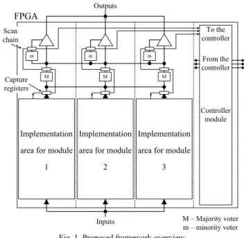
To avoid the effect of MBUs on the different modules [4], the three redundant modules of the user’s circuit should be placed in different columns of the FPGA. In our proposed framework we divided the FPGA vertically into four areas: three for the user’s circuit modules and a fourth area for plac-ing the detection-and-fix controller.
The interconnections between a module and its own In-put/Output Blocks (IOBs) should not cross other modules’area to avoid route networking share. The overall implementation scheme proposed is illustrated in figure 1.
When one or more faults appear in one of the modules or voters, the T-TMR implementation confines the fault and masks its existence, avoiding its propagation to the rest of the circuit. However, the cumulative effects of several faults in-duced over time may suppress the effectiveness of the con-finement and masking mechanism, allowing fault propagation. With the aim of detecting the emergence of faults a detection-and-fix controller is implemented in the fourth area defined on
the FPGA logic space. A detailed overview of this controller structure is shown in figure 2.
m M m M m M Implementation area for module
3
Inputs Outputs
Implementation area for module
1
Implementation area for module
2 FPGA To the controller From the controller Controller module Capture registers Scan chain M – Majority voter m – minority voter Fig. 1. Proposed framework overview.
The detection-and-fix controller is responsible for detecting data incoherencies, locating the faulty module and restoring the original configuration. This is done transparently, through partial reconfiguration of the affected module, without human intervention, since physical component replacement is not needed. As a result, a higher level of maintainability is achieved without implying the inoperability of the circuit.
Fig. 2. Overview of the detection-and-fix controller structure. IV. FAULT DETECTION, LOCATION AND MITIGATION This last point implies not only the existence of redundancy but also of a mechanism able to detect the emergence of an induced fault. It is very hard to detect a fault in a T-TMR im-plementation using traditional online test strategies, since the redundancy of the circuit masks its effect. In our approach, the detection of the faulty modules is done via three scan chains
that regularly capture the values at the outputs of the modules and voters.
A Boundary-Scan (BS)-like register [20] is used to imple-ment the scan chains, composed of simpler cells comprising only a capture / shift stage. The absence of the latch stage means that no delay is introduced in the signal’s path by the scan chain. To avoid capturing undefined values, the scan chain is updated synchronously with the system clock (assur-ing that modules or voters outputs will be in a steady state when they are captured).
The scan chain control signals are generated by the detec-tion-and-fix controller. This controller regularly updates the scan chains and shifts their contents, comparing the output values. Our framework uses three parallel scan chains, each covering a different module. This approach makes it easier for the controller to accurately diagnose which of the three mod-ule areas was affected by a fault, and to trigger its reconfigura-tion. More than one scan chain in parallel also has the addi-tional advantage of decreasing fault detection latency, since the shifting time is divided by the number of parallel chains (enabling more frequent capture operations).
The problem with this approach is that if a fault affects the content of a flip-flop, the output of its module will exhibit a wrong value, which will be captured by the scan chain, trig-gering the reconfiguration procedure of the module. However, reconfiguration will not correct the value stored in the flip-flop, and so, the error will persist. A feedback scheme to cor-rect faults in flip-flops, based on a majority voter that com-pares the outputs of the three replicated flip-flops and returns the correct value to the inputs is proposed in [17]. Further-more, this scheme results in the partition of the module in smaller logic blocks with voters in-between, which increases the robustness of the TMR in the presence of routing upsets without being of concern to floorplanning [9]. Yet, if a fault affects one of the majority voters, this voter will return to the input of its flip-flop a faulty value. This fault will be perma-nent and will be propagated to the inputs of the remaining voters, increasing the risk of fault accumulation and conse-quent circuit failure. A detection mechanism placed only at the outputs of the circuit may fail the detection of these faults if a fault occurs deep in the module logic.
Our proposal to solve this problem is to extend the scan chain to the inputs and outputs of each one of the flip-flops in the circuit, as illustrated in figure 3. In this way it is not only guaranteed that in case of a bit-flip in the flip-flop it will be correctly updated in the next clock cycle, but also that any functional fault affecting the majority voter will be detected through the scan chain, enabling to determine which module should be reconfigured. Furthermore, extending the scan chain to inside the module and wrapping on it the different combina-tional blocks and registers enables the precise location of the fault. This is an important feature considering the most recent SRAM-based FPGAs families, like the Xilinx Virtex-4 and Virtex-5. In these families the reconfiguration memory is di-vided into a number of rectangular regions, forming a grid. Each reconfiguration frame spans vertically only each one of the regions, instead of the whole FPGA as in earlier families.
It is therefore possible to limit the area to be reconfigured in case of fault detection to a single region due to the increased location precision of this approach [21].
Fig. 3. Implementation of the detection and state restoration mechanism in flip-flops.
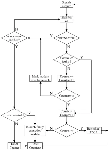
The sequence of tasks carried out by the detection-and-fix controller is represented in the flowchart shown in figure 4.
Signals capture Shift bit set Sb1=Sb2=Sb3 Controller faulty ? Scan chains’ last bit ? Counter= Counter+1 Countern= Countern+1 Countern>x Y Y N N N Y N Mark module area for reconf.
Counter>y Y Reconf. all FPGA Reset Counter Error detected ? Reset Countern Y Reconf. faulty controller/ module N N Y
Fig. 4. Detection-and-fix controller flowchart.
The sequence of tasks is continuously repeated in search of emerging faults (either in the controller or in the user mod-ules). The serial bitstreams captured through the scan chains are shifted to the internal controller where they are compared, bit-by-bit. When an incoherency is detected, the module where it was found is probably faulty.
Obviously, the controller and the scan chains may also be affected by SEUs. To ensure their correct operation, the con-troller is equally implemented using a T-TMR design and its combinational logic and voter output signals are also covered 304
by the scan chains, creating a self-verifiable circuit. The op-tion of concentrating the controller in only one area, despite being implemented in T-TMR, was taken to reduce complex-ity and the number of occupied CLB columns. However, since it occupies fewer slices than those available in each column, a convenient separation between modules was implemented.
The first bits of the scan chain belong to the outputs of the controller. If an incoherency is detected in those first bits, the controller will be fully reconfigured and reset at once. This procedure guarantees that the controller is working properly. While not being a critical component (concerning the func-tionality of the system), a fault-free controller is mandatory to maintain the reliability level of the whole system.
If an incoherency is detected on one of the bits captured by the scan chain, it is possible to restraint the origin of the fault to a limited area. The module is reconfigured after a parame-terizable number of detected faults (the ‘x’ and ‘y’ values on the flowchart of figure 4), even before reaching the last bit of the scan chains. A new capture operation is then performed and the verification process restarted.
Of course, if an upset affects the values shifted through the scan chain, this will falsify fault diagnosis and consequently trigger an extemporaneous partial reconfiguration of the sup-posedly faulty area. This operation, although unnecessary, will not affect the operation of the system.
A more complicated situation takes place if the structural configuration of the scan chains is affected by a fault. In this case, several neighboring bits will be disturbed, falsely indi-cating that a general failure in one or more modules occurred. Additionally, it won’t be possible to locate the place where the fault or faults emerged. Therefore, after the detection of a pa-rameterizable number of faults, either in the controller or in the modules, the controller undertakes a full dynamic recon-figuration of the FPGA, completely restoring the structural integrity of the scan chains.
The exact location of the fault enables the controller to acti-vate the partial reconfiguration and restoration of only a small area of the FPGA. An external memory stores the original partial configuration files concerning the four defined areas. These partial reconfiguration files may be subdivided into regions in case of using Virtex-4 or Virtex-5 devices. Due to the volatility of the FPGA configuration memory, this external memory was already necessary to hold the FPGA configura-tion bitstream (to be uploaded during system power up).
The inclusion of a fault detection mechanism improves the performance of the fault recovery procedure. In this case, scrubbing takes place only when necessary and on a well de-fined target. Bearing in mind the intervals between the occur-rence of SEUs, even in space applications [14], this solution enables considerable power savings when compared with pe-riodic “blind” full reconfiguration of, possibly, in the biggest FPGAs, tens of million bits. On the other way, a decrease in the scrubbing rate, while saving power, increases fault latency and therefore the risk of a system failure.
V. CASE STUDY
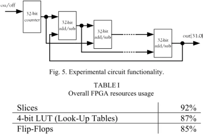
To evaluate the effectiveness of our approach, we devel-oped an experimental circuit based on a thirty two-bit counter and on a cascade of add/subtractor blocks, as illustrated in figure 5. The use of a cascaded configuration enabled the building of a large circuit, able to maximize FPGA occupa-tion, with a medium level of complexity but where the addi-tion of new add/subtractor blocks does not imply a decrease in its maximum frequency of operation, which enable to confirm the validity of the approach even with high performance cir-cuits. This circuit was implemented in a XC2V1500-based prototyping board, according to the rules defined in our pro-posed framework. The detection-and-fix controller used a total of 254 slices, distributed across two of the 40 available CLB columns, representing an area overhead of 5%. Notice that this overhead is constant and independent of the size or the com-plexity of the circuits implemented on the FPGA. The remain-ing 38 columns were divided in three areas of 12 columns each, leaving a total of 2304 slices available for the implemen-tation of each user module. Of these, 2184 slices were occu-pied by our circuit. The overall FPGA resources usage is summarized in table I. The extra two columns (remainder of the division of 38 by 3) were placed among the three areas of 12 columns, to reinforce protection against column-spanning MBUs.
Fig. 5. Experimental circuit functionality. TABLE I
Overall FPGA resources usage
Slices 92%
4-bit LUT (Look-Up Tables) 87%
Flip-Flops 85%
The incorporation with each flip-flop of a scan chain regis-ter implies an overhead of one LUT and one flip-flop each. An extra 3 slices are necessary per module output to capture the output value and the outputs of the corresponding majority and minority voter. The overhead is therefore dependent on the number of internal flip-flops and of outputs of the user circuit and not on its complexity.
In case of fault detection, the detection-and-fix controller initiates the partial reconfiguration of the affected area, by resolving the location address of the partial file to be config-ured. Our prototyping board uses System ACE [22] from Xil-inx to keep trace of the partial configuration files and to con-figure the FPGA. However, different kinds of interfaces may be used to provide the partial reconfiguration files, including remote sources. The partial reconfiguration files were gener-ated using the Foundation tools from Xilinx.
The dynamic reconfiguration of part or of the whole FPGA does not affect the operation of the functions whose function-ality is not changed, even if they are active and if its place-ment area is covered by the reconfiguration procedure. In other words, the mitigation procedure is completely transpar-ent.
The maximum speed of operation achieved by the detec-tion-and-fix controller was 221 MHz. Since capture operations must be synchronous with the operation of the user’s circuit, this is also the maximum frequency of operation of the user circuits. Our experimental circuit ran at 151 MHz.
Tests performed continuously over several days based on the insertion of faults through partial reconfiguration proved the effectiveness of the proposed concept. This process was automated using JBits [23]. Each fault insertion takes sixteen seconds. After several thousand fault insertions the circuit registered no system failures. It was able of autonomously recovered from the inserted faults. Currently, only pro-grammed bits are bit-flipped. The next step is the development of a random fault injection procedure to better simulate real working conditions, with an FPGA configuration frame being picked out randomly and a bit flip being also randomly exe-cuted in one of its configuration bits. The FPGA will then be partially reconfigured using the altered bitstream.
Notice that the insertion of faults on LUT affect not only the combinational blocks but also the voters at the outputs of the flip-flops, and, by consequence, due to the feedback path, the content of the flip-flop in itself. Despite the difficulty of directly injecting faults on flip-flops through partial reconfigu-ration in Xilinx Virtex FPGA devices, a technique was present in [24] to perform it.
VI. CONCLUSION
This paper presented a framework for the implementation of Self-Healing Radiation-Tolerant circuits on SRAM-based FPGAs. The approach is built around a customised TMR im-plementation, complemented with a mechanism for the detec-tion of faults coupled with a detecdetec-tion-and-fix controller able to determine the location of the fault and of promoting the reconfiguration of the affected area.
Several issues addressing the effectiveness of TMR to cope with radiation-induced faults in FPGAs were reviewed and discussed to support the option of associating T-TMR to a careful floorplaning and to dynamic reconfiguration as the most effective approach to mitigate radiation-induced faults in FPGAs. To avoid system failure due to fault accumulation a complementary detection-and-fix controller mechanism was proposed, with the aim of restoring the proper operation of the modules when a fault is detected. Selectively doing so limits power consumption due to repetitive ‘blind’ scrubbing with its erratic performance.
A practical case-study enabled the quantification of the overhead of our proposed solution and the assessment of its effectiveness. Further work is being done to improve the evaluation methodology.
REFERENCES
[1] L. Sterpone, M. Violante, “Analysis of the Robustness of the TMR Ar-chitecture in SRAM-Based FPGAs”, IEEE Trans. on Nuclear Science, Vol. 52, No. 5, pp. 1545-1549, October 2005.
[2] M. Ceschia et al., “Identification and Classification of Single-Event Upsets in the Configuration Memory of SRAM-Based FPGAs”, IEEE
Transactions on Nuclear Science, Vol. 50, No. 6, pp. 2088-2094,
De-cember 2003.
[3] M. Bellato et al., “Evaluating the effects of SEUs affecting the configu-ration memory of an SRAM-based FPGA”, Proc. of the Design,
Automa-tion and Test in Europe Conf., pp. 584-589, 2004.
[4] H. Quinn et al., “Radiation-Induced Multi-Bit Upsets in Xilinx SRAM-Based FPGAs”, Proc. Military and Aerospace Appl. of Prog. Logic
De-vices Conf., 2005.
[5] M. French et al., “Radiation Mitigation and Power Optimization Design Tools for Reconfigurable Hardware in Orbit”, Proc. of the Earth-Sun
System Technology Conference, 2005.
[6] C. Carmichael et al., “SEU Mitigation Techniques for Virtex FPGAs in Space Applications”, Proc. Military and Aerospace Applications of
Prog. Logic Devices Conf., 1999.
[7] E. Fuller et al., “Radiation Testing Update, SEU Mitigation, and Avail-ability Analysis of the Virtex FPGA for Space Reconfigurable Comput-ing”, Proc. Military and Aerospace Appl. of Prog. Logic Devices Conf., 2000.
[8] M. G. Gericota et al., “A self-healing real-time system based on run-time self-reconfiguration”, Proc. of the 10th IEEE Conf. on Emerging
Tech-nologies and Factory Automation, pp. 19-22, 2005.
[9] F. Lima Kastensmidt et al., “On the Optimal Design of Triple Modular Redundancy Logic for SRAM-Based FPGAs”, Proc. IEEE Design,
Automation and Test in Europe, pp. 1290-1295, 2005.
[10] L. Sterpone, M. Violante, “A New Reliability-Oriented Place and Route Algorithm for SRAM-Based FPGAs”, IEEE Trans. on Computers, Vol. 55, No. 6, pp. 732-744, June 2006.
[11] M. Rebaudengo et al., “Simulation-based analysis of SEU effects on SRAM-based FPGAs”, Proc. of the 12th Intl. Conf. on Field-Prog.
Logic and Applications, pp. 607-615, 2002.
[12] M. Wirthlin et al., “The Reliability of FPGA Circuit Designs in the Pres-ence of Radiation Induced Configuration Upsets”, Proc. 11th IEEE
Symp. on Field-Prog. Custom Computing Machines, pp. 133-142, 2003.
[13] G. M. Swift et al., “Dynamic testing of Xilinx Virtex-II field program-mable gate array (FPGA) input/output blocks (IOBs)”, IEEE Trans. on
Nuclear Science, Vol. 51, No. 6, pp. 3469-3474, Dec. 2004.
[14] M. Gokhale et al., “Dynamic reconfiguration for management of radia-tion-induced faults in FPGAs”, Proc. 18th Intl. Parallel and Distributed Processing Symp., pp. 145-150, 2004.
[15] M. Abramovici et al., “Using Roving STARs for On-Line Testing and Diagnosis of FPGAs in Fault-Tolerant Applications”, Proc. Intl. Test
Conf., pp. 973-982, 1999.
[16] M. G. Gericota et al., “Active Replication: Towards a Truly SRAM-based FPGA On-Line Concurrent Testing”, Proc. of the 8th IEEE Intl.
On-Line Testing Workshop, pp. 165-169, 2002.
[17] Triple Module Redundancy Design Techniques for Virtex FPGAs,
XAPP 197 Application Note, Xilinx, 2001.
[18] P. K. Lala, Self-Checking and Fault-Tolerant Digital Design. San Fran-cisco, CA: Morgan Kaufman Publishers, 2001.
[19] TMRTool, available at:
http://www.xilinx.com/ise/optional_prod/tmrtool.htm
[20] IEEE Standard Test Access Port and Boundary Scan Architecture (IEEE Std 1149.1), IEEE Std. Board, June 2001.
[21] Virtex-5 FPGA Configuration User Guide 2006, available at: http://direct.xilinx.com/bvdocs/userguides/ug191.pdf
[22] System ACE MPM Solution, Product Specification, Xilinx, 2003. [23] S. A. Guccione et al., “JBits Java based interface for reconfigurable
computing”, Proc. 2nd Military and Aerospace Appl. of Prog. Devices
and Technologies Conf., 1999.
[24] L. Antoni et al., “Using Run-Time Reconfiguration for Fault Injection Applications”, IEEE Transactions on Instrumentation and Measurement, Vol. 52, No. 5, pp. 1468-1473, October 2003.