Shiv Jyotindra Bhudia
Bachelor in Micro and Nanotechnologies Engineering
Static and dynamic modelling for IGZO-TFT
devices with high-
κ
multilayer dielectric.
Dissertation submitted in partial fulfillment of the requirements for the degree of
Master of Science in
Micro and Nanotechnology Engineering
Adviser: Dr. Arokia Nathan, Full Professor, University of Cambridge
Co-adviser: Pedro Barquinha, Assistant Professor, Faculty of Sciences and Technology Nova University of Lisbon
Examination Committee
Chairperson: Dr. Luís Miguel Nunes Pereira Raporteurs: Dr. Arokia Nathan
Dr. João Carlos da Palma Goes
Static and dynamic modelling for IGZO-TFT devices with high-κ multilayer dielectric.
Copyright © Shiv Jyotindra Bhudia, Faculdade de Ciências e Tecnologia, Universidade NOVA de Lisboa.
A Faculty of Sciences and Technology e a NOVA University of Lisbon têm o direito, per-pétuo e sem limites geográficos, de arquivar e publicar esta dissertação através de exem-plares impressos reproduzidos em papel ou de forma digital, ou por qualquer outro meio conhecido ou que venha a ser inventado, e de a divulgar através de repositórios científicos e de admitir a sua cópia e distribuição com objetivos educacionais ou de investigação, não comerciais, desde que seja dado crédito ao autor e editor.
This document was created using the (pdf)LATEX processor, based in the “novathesis” template[1], developed at the Dep. Informática of FCT-NOVA [2].
Acknowledgements
This thesis only becomes a reality with the kind support and help of many individuals, that somehow made a difference to me in the past five years. For this reason, I would like to sincerely thank:
To my advisor Prof. Arokia Nathan, for having me in his group of excellence at one of the most prestigious universities of the world. I am very grateful for all the support and guidance that were given to me throughout this work and also his tremendous humble concern for my well being during this stay I had at the University of Cambridge. I can surely say that I had one of the best moments of my life there.
To my co-advisor Prof. Pedro Barquinha. I am very proud and honoured of having him not only as advisor but also as a mentor. For all the support and guidance that he gave me through this journey even at the hardest times. He surely will serve as an inspiration for my life.
To Prof. Rodrigo Martins, for building up the foundation of one of the best working environments of the world at this tiny Portugal. With excellent laboratories and work ethics of their collaborators many international partnerships are established. Including the one that allowed me to work at the University of Cambridge that would be impossible to me elsewise.
To Prof. Luís Pereira and Diana Gaspar for the tremendous organization of the BET-EU project which allowed me to do this work at one of the world leading research groups at zero expenses. Which is a tremendous privilege to anyone at any part of the world and I consider myself very lucky of having this opportunity.
To the BET-EU project (Materials Synergy Integration for a Better Europe, Grant agree-ment No. 692373) for the funding that allowed me to work overseas.
To Dr. Xiang Cheng, for all the availability and scientific knowledge that he gave me to produce this work, and also the friendship we built.
To the Hetero-Genesys staff, a truly multicultural group that received me as member of their family from day one.
To Ana, Joana and Crespo my Cambridge family. The great moments we shared together will definitely last forever. All the family like dinners, nights out, UK trips, philosophical conversations will truly be missed.
To "dois amigos e um indiano"a friendship that I will keep and nourish for a lifetime. All the Wild experiences we had together and hopefully build new ones.
To Viorel and Inês, Alexandre, Alexandra, David, Cátia, Sara, Peres, Chico, Daniela, Jolu, Afonso and Marco for all the great parties, profound talks and phenomenal moments we spend together thought this years.
To my family: my sisters, mother, father, my aunts and uncle, grandmother, for all the
love and devotion that was given to me that shape who I am today. Thank you.
Abstract
Indium-Gallium-Zinc-Oxide thin-film transistors (IGZO-TFT) are a strong alternative technology for the current trend of Si based field-effect transistor (FET) for flat-panel display backplane and internet of things internet of things (IoT). In these applications, comprehensive understanding and accurate modelling of thin-film transistor (TFT) is compulsory for systematic circuit design.
In this study, IGZO-TFTs with high-κ multilayer dielectric, which were previously fabricated at CENIMAT/I3N Portugal are characterized in the University of Cambridge at the department of electrical engineering. Alongside this characterization, it is developed a compact static model that is capable of describing above-threshold linear behaviour. This model is based on physical parameters and also accounts the effects of contact resistance in source and drain terminals. Furthermore, it is developed a dynamic small signals model, based on conventional FET models and its validity is studied with the help of S-Parameters and capacitance-voltage characteristics (C-V) characteristics.
The great advantage of the developed models, in both static and dynamic aspects, is the low number of parameters required to be extracted physically with good fitting results. This can empower new users that are not so familiar with the modelling aspect to design simple electrical circuits with IGZO-TFTs.
Keywords: IGZO, TFT, Static models, Dynamic models, Compact models, small signal.
Resumo
Os transistores de filme fino baseados em óxidos de Índio Gálio e Zinco (IGZO-TFTs) são uma tecnologia alternativa muito interessante para a atual tendência de transistores de efeito de campo, que é baseada no Silício, para o painel traseiro de mostradores planos e aplicações em internet das coisas (IoT). Nestas, a compreensão exaustiva e uma boa mode-lagem do comportamento de TFTs são requisitos obrigatórias para a projeção sistemática de circuitos.
Neste estudo, os TFTs IGZO com dielétrico multicamadas de alta permissividade, que foram fabricados à posteriori nos laboratórios CENIMAT / I3N Portugal, são carac-terizados no departamento de engenharia eletrotecnia da Universidade de Cambridge. Juntamente com essa caracterização, desenvolve-se um modelo estático compacto que é capaz de descrever o comportamento linear acima da tensão limiar de condução. Este modelo é baseado em parâmetros físicos e também contabiliza os efeitos da resistência de contato nos terminais de fonte e dreno. Além disso, é desenvolvido um modelo dinâmico de pequenos sinais, baseado em modelos de transistores de efeito de campo convencionais e a sua validade é estudada com a ajuda das características dos Parametros-S e curvas de capacidade tensão.
A grande vantagem dos modelos desenvolvidos, tanto no modelo estático assim como no dinâmico, é o baixo número de parâmetros necessários para serem extraídos fisica-mente. Isso pode capacitar novos usuários que não estão tão familiarizados com o aspecto de modelagem para conseguirem projetar circuitos elétricos simples com esta tecnologia.
Palavras-chave: IGZO, TFT, modelagem, modelos estáticos, modelos dinâmicos, modelos
compactos, pequenos sinais
Contents
List of Figures xiii
List of Tables xv
List of Symbols xvii
Acronyms xix
Objectives 1
Work Stucture 1
1 Introduction 3
1.1 Motivation . . . 3
1.2 The beginnings of device modelling . . . 3
1.3 Compact models . . . 4
1.3.1 Physical based compact models . . . 4
1.3.2 Empirical based compact models . . . 6
1.4 Small-signal modelling . . . 6
1.4.1 Midband small-signal model . . . 7
1.5 State of the art in TFT modelling . . . 8
2 Methodology 9 2.1 IGZO-TFTs fabrication and structure overview . . . 9
2.2 Static model . . . 10
2.3 Dynamic model . . . 11
3 Above-Threshold parameter extraction and Linear Model 13 3.1 Threshold Voltage,VT . . . 13
3.1.1 Results . . . 14
3.2 Contact resistance,RDSW and∆L . . . 14
3.2.1 Results . . . 16
3.3 Power parameter,α . . . 16
3.4 transconductance parameter,K . . . 17
3.5 Model representation . . . 17
3.5.1 Discussion of Results . . . 18
4 Small-signal model 21 4.1 High Frequency TFT model . . . 21
CO N T E N T S
4.1.1 Measurement setup . . . 22
4.1.2 Dominants-parameters for measurement and analysis . . . 23
4.2 S-Parameters . . . 25
4.2.1 S11theoretical analysis . . . 25
4.2.2 S21theoretical analysis . . . 26
4.3 Model validation . . . 27
4.3.1 Pre requirements . . . 27
4.3.2 Model representation . . . 28
5 Conclusions and future prospectives 31
Bibliography 33
A Appendix 37
B Appendix 39
C Appendix 41
List of Figures
1.1 Small-signal model for a general 3 terminal device in mid-band frequency,
also known as hybrid-pi model [12]. . . 7
2.1 TFT device structure used in this work: staggered bottom gate, top-contact . 9 2.2 Equivalent circuit of static TFT model. . . 11
3.1 Second derivative method forVTextraction in real and Ideal FET. . . 14
3.2 Extracted values ofVT for TFT devices with W ∼ 20µm. The black plot is for IDS(VGS) characteristics, while the blue plot is the second derivative of the black plot. The error bar comes from the three replicas measured. A) L∼20µm; B)L∼40µm; C)L∼80µm; D)L∼160µm. . . 15
3.3 BvsAplot forRDSand∆Lextraction . . . 16
3.4 IDS,lin gm,lin vs (VGS−VT) for alpha extraction (R 2= 0.998). . . . 17
3.5 A−1/(a−1)vsVGS−VTplot forK parameter extraction . . . 18
3.6 Comparison between theIDSvsVGScharacteristics for the measured devices and developed model based on Eq. (2.5). TheVDS is maintained at 5 mV, to ensure the linear region . . . 19
3.7 Output characteristics forL∼20µm andW ∼20µm. . . . 19
3.8 Output characteristics forL∼160µm andW ∼20µm. . . . 20
4.1 Low frequency small signal MOSFET model adapted for TFT . . . 21
4.2 High frequency small signal MOSFET model adapted for TFT. . . 22
4.3 Measurement set-up for s-parameters andfT. . . 23
4.4 Equivelent circuit forS11andS21measurements. . . 24
4.5 Equivalent circuit to obtainZLforS11expression. . . 25
4.6 C-V characteristics for 320µm/20µm TFT . . . . 27
4.7 Magnitude and phase measurement and simulation forS11for TFT with W/L= 160/20. . . 28
4.8 Magnitude and phase measurement and simulation forS21for TFT with W/L= 160/20. . . 29
4.9 h21simulation and measurement results forfTdetermination. . . 29
A.1 Illustrative procedure forRDSextraction used in this work. . . 37
B.1 RTvsVGS−VT, for differentLs.In order to produce an arbitrary value ofVGS−VT for later plots. The best fit option is used to create a mathematical function that can return any value ofRT given aVGS−VT. The function generated is based on exponential decay of 3rd order. . . 39
L i s t o f F i g u r e s
B.2 RTvsLfor differentVGS−VT. As we can see the from the amplification near the intersect, makes hard to extractLeffandRDS. . . 40
C.1 Magnitude and phase measurement and simulation forS11for TFT with W/L= 320/20. . . 41 C.2 Magnitude and phase measurement and simulation forS21for TFT with W/L=
320/20. . . 41 C.3 h21simulation and measurement results forfT determination, for TFT with
W/L= 320/20. . . 42
List of Tables
3.1 ExtractedVTvalues for different channel lengths . . . 14 3.2 Extracted values forRDSW and∆L . . . 16 3.3 Summary of all parameters extracted for above-threshold linear model . . . 18
4.1 Extracted values for s-parameters representation . . . 28
List of Symbols
NA acceptor concentration.
Vch channel potential.
q charge of an electron.
RDS combined contact resistance from drain and source sides.
IDS current flow between drain and source.
ntr density of occupied traps.
κ dielectric constant.
∆L Difference between mask channel length and effective channel length.
ND donor concentration.
VD drain voltage.
Leff effective channel length.
ε electric permittivity of the material.
ψ electric potential.
Rn electron recombination rate.
Gn electron generation rate.
Jn electron current density.
Rp hole recombination rate.
L I S T O F S Y M B O L S
Gp hole generation rate.
Jp hole current density.
α power parameter.
VS source voltage.
VT threshold voltage.
K transconductance parameter.
Acronyms
CAD computer aided design.
C-V capacitance-voltage characteristics.
CVU capacitance-voltage unit.
DOS density of states.
ENA Keysight E5061B network analyser.
FET field-effect transistor.
I-V current-voltage characteristics.
IGZO Indium-Gallium-Zinc-Oxide.
IGZO-TFT Indium-Gallium-Zinc-Oxide thin-film transistors.
IoT internet of things.
RPI Rensselaer Polytechnic Institute.
SPICE Simulation Program with Integrated Circuit Emphasis.
TFT thin-film transistor.
Objectives
Device modelling can be very tedious, with large amount of parameters to be extracted as well different types os measurements that they might require. Furthermore, the rapid evolving device structure and materials in the TFT family demand for simple compact models that can serve as a platform for simple circuit design. This thesis work, which is part of the project BET-EU (Materials Synergy Integration for a Better Europe) under the Grant agreement No. 692373, is concerned with the viability of developing compact mod-els for IGZO-TFTs with high-κ multilayer dielectric based on other existing models for rapid and simple modelling. Moreover the project is aimed to develop an above-threshold and small-signal model that require minimal number of direct measurements which may serve as a platform for simple circuit design applications.
Work Stucture
This work is organized as follows: The motivation introduces the relevance of IGZO-TFT technology and the importance of developing compact models to open doors for this technology to flourish in new applications; It is followed by the introduction where it is explained how device modelling came to be, what are compact models and how they are subdivided, small signal in three terminal devices and lastly the state of the art in TFT modelling. Chapter 2 explains the overall work-flow and methodology used in this project. Chapters 3 and 4 describe each of the studies. Chapter 3 includes the procedure for parameter extraction followed by the model representation. Chapter 4 includes all the work done on the development of the small signal model. Finally, Chapter 5 summarizes all the work done on TFT compact modelling, moreover some future ideas are presented.
1
Introduction
1.1 Motivation
FETs are developed using a wide range of semiconductor materials, with the most pre-dominantly employed being the Silicon. FETs applications end up in many technological products and lead to performance increase and reduction in size and weight, with increas-ing miniaturization [1]. Ever since the Si FET technology started to mature a continuous progress has been made year after year in both large-scale integrated circuits and flat-panel displays.
Given this circumstances Indium-Gallium-Zinc-Oxide (IGZO) emerged as one of the most competitive alternative for such applications. The combination of low processing temperature, transparent nature, good uniformity even in large areas and excellent elec-trical properties (typically having the channel mobility higher in one order of magnitude when compared toα-Si) have proven to be a great asset for this technology.
In fact, it took only nine years after the first working prototype of IGZO-TFT, pub-lished by Hideo Hosono’s group, to come up with a commercially available product by Sharp. The IGZO-TFTs were employed in the display of their flagship smart-phone [2].
Despite the rapid growth for IGZO in flat-panel displays, the same is not observed in other potential applications, such as IoT, augmented displays and wearables. Great part of it could be explained due to circuit design complexity. In one hand, the circuit design in flat-panel displays is limited to a few repetitive circuits, in that sense designing and optimizing is simple here. On the other hand, TFTs have a wider range of materials, device structure and processing methods when compared to conventional Si technology. For this reason the creation of a universal behavioural device model for TFTs is a big challenge [3].
The combination of these factors motivate the development of simple and accurate device behavioural models for a more specific group TFTs, that can have potential appli-cation in computer aided design (CAD) tools for new circuit designs.
1.2 The beginnings of device modelling
In the early days, when transistors were not microscopic, the circuit design was heavily empirical. With discrete elements such as capacitors, inductors, resistors and transistors at the disposal of the designer, he would build and test his circuit onto a circuit board. The design procedure would start with some simple electrical concepts and the “tweak-ing”(sizing in integrated circuits) would be made by simply replacing elements in value or type till the specifications were met. With the emergence of integrated circuits this simple procedure was no longer possible, this may be attributed to some key reasons.
C H A P T E R 1 . I N T R O D U C T I O N
Firstly, the integrated elements are now embedded in a common substrate, which makes the replacement difficult to practically impossible. Alongside this the common substrate to all elements will naturally form parasitic components that are not so easy to account for, empirically.
The second major reason comes along with “the size of both worlds”. In discrete elements, the different encapsulated components are linked to each other through bread-board tracks which separate them in tens of millimetres. While in the integrated case, these connections are in the micron level. This shorter distance, makes self-inductances of the interconnection lines, on integrated circuits, non-neglectable. Besides that to pro-duce an inductive element with small tolerance is not so easy, many times it has to be implemented with an external element.
In the present days, designers resort to many CAD tools such as Simulation Program with Integrated Circuit Emphasis (SPICE), Spectre etc., for their circuit analysis. These softwares contain mathematical models that are capable of describing quantitatively the terminals behaviour of an element. With this the designer can forecast the behaviour of a desired circuit without the need of its fabrication, reducing time and cost. How well the forecast is done, is entirely up to the models behind the program. For this reason it is very important to understand how these models behave.
1.3 Compact models
Compact models are generally aimed at providing accurate device behaviour, which covers all working regions, for circuit simulation. The accuracy of a compact model does not only depend on the set of mathematical equations, but also on the accuracy of the numerical constants in these equations. In device modelling these constants are called parameters, which can be extracted through physical measurements, or in the impossibility of this, with numerical simulations. So, the model developer must not only account for the model equations but also for the parameter values.
While the main goal is accuracy, it is also necessary to account for speed of simulation. Some circuits may contain millions or more transistors, in such cases it is imperative that the mathematical model of each element is as simple as possible, otherwise the CPU time and/or memory storage will be prohibitive [4].
The compact models can be subdivided in two major groups, physical and empirical models which will be discussed in the next sections.
1.3.1 Physical based compact models
Physical based compact models are defined when the equations that describe the model are derived from device physics. These equations are based on analytical functions, where explicit results are desirable. The analyticity is very important because it grantees that the function is infinitely differentiable, otherwise the computer program could lead to
1 . 3 . COM PAC T M O D E L S
numerical instabilities. Especially in time based analysis, the calculation of harmonic-distortion often require the existence of derivatives.
Since the parameters have physical meaning and in general case have multiple ex-traction methods, they can help to check the correctness of the parameter exex-traction procedure.
The major drawback of these expressions is that they generally only apply for a specific range of voltage bias condition, outside of those ranges other expressions need to be used. In order to have good convergence and smooth transition between the various regions, a mathematical smoothing procedure is used, typically in the form of harmonic averaging. Other than that, these models take long time to be developed even with experienced researchers (several months to years) [5].
1.3.1.1 Foundation for physically based compact models
Having established the general characteristics of physically based compact models, we now analyse the building blocks that constitute the foundation of most of these models.
A semiconductor can be described by a set of coupled non-linear partial differential equations, more specifically Poisson’s equation for drift diffusion
∇2ψ=−q
ε (p−n+ND−NA+ntr) (1.1)
and the current continuity equation for carrier distribution
∂n
∂t =∇ ·Jn+Gn−Rn ∂p
∂t =−∇ ·Jp+Gp−Rp
(1.2) where
Jn=qµnnE+qDn∇n Jp=qµppE−qDp∇p
(1.3)
In Eq. (1.1),ψis the electric potential,qis the charge of an electron, µn andµpare the mobility of the electrons and holes,εis the electric permittivity of the material,nand prepresent the concentration of electrons and holes, respectively, NA andND are the acceptor and donors concentration, respectively, andntris the density of occupied traps. In Eq. (1.2),Jn andJp are electron and hole current densities, Gn andGp represent the generation rates, Rn andRp are the recombination rates. Lastly, (1.3) the first part of the sum is related to the drift (proportional to electrostatic field), and the second part to diffusion (proportional to gradient of the carrier density) [6].
Dealing with these set of equations is somewhat cumbersome, and for the general case of device structures they will not lead to closed-form solutions. The best results are achieved with numerical methods which, as seen previously, come at the cost of using many computational resources.
In 1952 Shockley introduced an important simplification to this problem [7], by real-izing that the rate of change of the electrical field is much greater in one dimension (gate
C H A P T E R 1 . I N T R O D U C T I O N
to active layer) than the other (source to drain). By decouplingxandydimensions, the problem simplifies into two 1-D problems. One first equation describes the number of carriers in the channel, while the second equation describes the carrier flow from source to drain. Later, in 1966 H.C.Pao and C.T. Sah [8], based on this concept, proposed a MOSFET model that has been a benchmark ever since to many compact models, since it has only a few assumptions that are transversal to many other FET technologies [9].
By assuming, that the hole current and the recombination/generation can be ne-glected, the expression that gives the currentIDS that flows from drain and source is
IDS=µWL Z VD
VS
Q dVch (1.4)
In Eq. (1.4), W is the width of the transistor,Lis the length,VSandVD are source and drain voltages,Qis the integrated mobile charge, andVchthe channel potential.
From here, two main classes of models, that are capable of describing IDS have emerged. The first kind, known as charge based models, define IDS with an induced charge term. While the second type, surface-potential based models, assume a density of states (DOS) profile to solve the Poisson’s equation, andIDSis expressed in terms of surface potential at source and drain [10].
1.3.2 Empirical based compact models
In the other spectrum we have empirical based compact models, here the expressions are based on mathematical curve-fitting or polynomial approximations to describe the behaviour of any kind of transistor. Since the model does not require deep understanding of the device physics, the development time is greatly shorten. However, without proper understanding of the underlying device physics, the resulting parameters could be large and unmeasurable trough extraction procedure. In practice purely empirical models do not exist, the models used in simulation are often a combination of terms and coefficient that are physical and empirical.
1.4 Small-signal modelling
While the general case in the development of transistor models is the in-depth under-standing of the device physics, there is another important element for circuit analysis (which electrical engineers very much like to use), the small-signal model. In small-signal analysis non-linear devices, such as the transistor, are described with linear equation un-der certain constrains of biasing. If the AC signal is small enough relatively to the bias voltage, then the whole signal can be represented as a DC signal with small perturbations. This small non-linear effect can then be approximated by the Taylor expansion series near the biasing point by its first order partial derivative. Finally, the partial derivative trans-lates into variations of impedance throughout the signal, and can be used to represent a
1 . 4 . S M A L L- S I G N A L M O D E L L I N G
linear equivalent circuit giving the response of the real device under a small AC signal [11].
1.4.1 Midband small-signal model
For a general three terminal device with G,S and D as the arbitrary terminals, the current-voltage characteristics (I-V) equation can be defined as follows :
ID=f1(VGS, VDS)
IG=f2(VGS, VDS) (1.5)
For small changes ofVGS andVDS, the current differences would approximately follow the first order partial derivatives of both current functions respectively
dID= ∂VGS∂f1 dVGS+ dID=∂VDS∂f1 dVDS dID= ∂VGS∂f2 dVGS+ dID=∂VDS∂f2 dVDS
(1.6)
Now by assuming good linearities at the bias point, the partial derivatives are simplified to mere constants as follows
id=gm1vgs+vdsro1
id=vgsro2 +gm2vds (1.7)
The coefficientvdsforid andvgsforigcan be represented as passive components, in this casero1 andro2 respectively. Whilevgs forid andvgs forid is only representable with active component, a voltage controlled current source (transconductance in the form of gm1andgm2are used). The small signal representation of these equations for mid-band range can be seen in Fig. 1.1.
S
D
G
1 or
2 or
1 m gs g v 2 m dsg v
di
gi
dsv
gsv
Figure 1.1: Small-signal model for a general 3 terminal device in mid-band frequency, also known as hybrid-pi model [12].
For simplification purposes in many FET devices it is considered thatVDS does not affectIGand thero2is high enough that gate leakage current can be neglected, therefore the gate and source terminals are presented as open-circuit.
C H A P T E R 1 . I N T R O D U C T I O N
1.5 State of the art in TFT modelling
In recent years, many efforts have been made towards the physical approach in the hopes of developing simple and accurate models. From all the different families of TFTs,α-Si is the most well-studied. Numerous models have been published based on the study of DOS, which are capable of describing both static and dynamic behaviours in various working regions [13–15]. The effects of traps on VT shift [16] and current leakage [17] have also been implemented in model design. In fact a commercial standard is available which captures most of device properties, called Rensselaer Polytechnic Institute (RPI) model. Also it has been implemented the EKV model, designed initially for the MOSFET, for this family of transistors [18].
For organic TFTs, many developments have been made based on the conduction mech-anism in these devices [19, 20]. However, due to the high variety of materials and struc-tures, the physical mechanism also differs. In that manner the effort has gone towards a more unified but less physical model [21].
As for metal-oxide TFTs modelling attempts are still in their primordial. Despite that, there has been reported good results with the use of RPI models, with minor adjustments, in IGZO devices [22]. In 2016 a model based on effective DOS extraction has been proposed for Verilog-AMS and SPICE aplications, called CAMCAS model that focuses in oxide-TFTs with potential extendibility to other families [3].
In the other spectrum, there has been developed empirical models based on neural networks that are design to make the model development as fast as possible [23, 24].
2
Methodology
In this chapter, it will be addressed the overall work-flow of the project. In the first instance the device fabrication and structure, prior to this project, are evoked. Following that, some guidelines about the development of both dynamic and static models are discussed.
2.1 IGZO-TFTs fabrication and structure overview
Prior to this project, IGZO-TFT with high-κ multilayer dielectric were fabricated, at CENIMAT/I3N Portugal. The TFTs were produced according to a staggered bottom gate, top-contact structure on Corning glass substrates (Fig. 2.1). RF magnetron sputtering was used to deposit thin films of Molybdenum as electrodes, IGZO (1:2:2 In:Ga:Zn atomic ratio) as active layer and Ta2O5/SiO2 for the multilayer dielectric. The patterning is achieved through lift-offprocess, and to finish offa post-deposition annealing is done in air atmosphere at no more than 200 °C. The characteristic that stands out is the multi-layer dielectric, which is conceived to have high-κ and high bandgap energy to minimise problems of instability, gate-leakage and hysteresis. For a more detail explanation on the fabrication and characterization of similar devices [22] is an excellent read.
Source Drain Substrate Gate Active Layer Dielectric Corning Glass Corning Glass Molybdenum Molybdenum TiO5 TiO5 SiO2 SiO2 IGZO (1:2:2) IGZO (1:2:2) Source Drain Substrate Gate Active Layer Dielectric Corning Glass Molybdenum TiO5 SiO2 IGZO (1:2:2)
Figure 2.1: TFT device structure used in this work: staggered bottom gate, top-contact
The core work of this thesis is done at the Hetero-Genesys Laboratory of the Univer-sity of Cambridge. They have a multi-disciplinary research environment including the development of compact models for TFTs. In that sense, all the characterization and development of models for the devices in study is done at this location.
C H A P T E R 2 . M E T H O D O LO G Y
2.2 Static model
As seen in chapter 1.3.1, the development of a new physical based compact model can take many months or even years. In that sense, the strategy here was to find a good compact model that was already developed starting with similar assumptions of our working devices. The first good candidate is the MOSFET level 1 model that has the following equations, for Triode region (VGS> VTand 0< VDS<[VGS−VT])
IDS=KWL
(VGS−VT)VDS− VDS2
2 (2.1)
and for Saturation (VDS> VGS−VTandVGS> VT)
IDS=K2 WL (VGS−VT)2 (2.2)
In Eq. 2.1 and Eq. 2.2 theK is the transconductance parameter,W andLare the width and length of the channel.
Having seen the MOSFET equations forIDS, and after some quickIDS(VGS) measure-ments in the saturation region we observed that the TFT devices did not perfectly obey to this proportionality:IDS∝(VGS−VT)2. This is mainly due to velocity saturation effects [25], so a more general power parameter (α) is used instead of 2. Besides this, the other major concern in TFTs comes from big contact resistance (RDS). There is also another consideration done, that comes along with the channel length. When fabricating a TFT device theLvalue is typically attributed to the design mask value. However due to the fabrication process itself the channel length may not correspond exactly to this value. This variation (∆L) can be quantified empirically and it is added to the maskLvalue. This
result into the effective channel length,Leff.
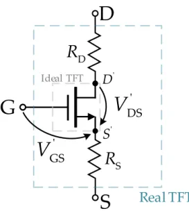
The static model for TFT can be defined as the structure shown in Fig. 2.2 where the I-V characteristics are modelled for the internal transistor and theRDSin both contacts are accounted separately.
Based on [26] model which accounts for these effects, the primed voltagesV′ DS and VGS′ can be defined as follow:
VDS′ =VDS−IDS(RS+RD)
VGS′ =VGS−IDSRS (2.3)
The drain-source current for linear regime (IDS,lin) can be written as a function ofVGS′ as
IDS,lin=K W Leff
VGS′ −VT α−1
VDS′ −
1−1 α
(V′
DS)α
(2.4)
Withα= 2 this equation simplifies into Eq. (2.1). If we now consider thatRS=RD= RDS2 , the final equation forIDS,lincan be obtained by substituting (2.3) into (2.4)
IDS,lin=K W Leff
"
VGS−VT−IDSRDS2
α−1
(VDS−IDSRDS)−
1−1
α
(VDS−IDSRDS)α #
(2.5)
2 . 3 . DY N A M I C M O D E L
S
D
G
Ideal TFT
Real TFT
'S
'D
DR
SR
' DSV
' GSV
Figure 2.2: Equivalent circuit of static TFT model.
However for parameter extraction purposes, a simplification is necessary. Considering
IDSRDS
2 ≈0.5VDSand by forcingVDSto be very small, in comparison toVGSandVT, the Eq.
(2.5) can be simplified into:
IDS,lin=KLW eff
(VGS−VT−0.5VDS)a−1(VDS−RDSIDS) (2.6)
For device modelling, the linear region is the most important for parameter extraction, furthermore the saturation regime can be deduced from this equation, by substituting VDS =αsat(VGS−VT). The term αsat is applied as a correction parameter, since in real devices the transition between linear to saturation is not always at VDS = (VGS−VT). Another strategy, is to consider a smooth transition from VDS to VGS−VT, this can be achieved with harmonic averaging methods. In fact this second method is chosen for this project, due to its simplicity.
With a satisfactory model, the different parameters were extracted, this will be pre-sented in later chapter 3.
2.3 Dynamic model
For this part of the project, a small signal model based on MOSFET devices was modelled, the main challenge here was to find a common ground that could validate or discard the use of MOSFET small-signal model for the devices in study, this gains higher importance at high frequencies where parasitic capacitances are no longer neglected. The common ground was found with the calculation of unit-gain frequency which is equivalent toh21 parameter, this last one can be indirectly measured through S-parameters. For a simpler understanding of this part, the full procedure and discussion is presented in a single chapter (Chapter. 4).
3
Above-Threshold parameter extraction and
Linear Model
In this section, it is extracted the parameters required to describe the TFT in the linear region for static modelling (Eq. (2.6)). These parameters are K, Leff, VT, α andRDS.
For the measurement set-up it is used a Keithley 4200 semiconductor characterization system to measure I-V characteristics. It is considered TFTs withW ∼20µm and different channel lengths, L∼20;40;80;160 µm, the reasoning for this design of experiment is
mainly due toRDS extraction. To minimise measurement errors, each sized TFT has 3 replicas making a total of 12 transistor for measurement. The DC bias conditions are chosen to beVDS= 5 mV and a voltage sweep is performed between the gate and source from−5 to 15 V with an incremental step of 0.1 V, this ensures the TFT to work in linear region. For the output characteristics it is performed a voltage sweep fromVDS= 0 V to 15 V with 0.1 V increments, for each value ofVGS. For multiple voltagesVGShas steps of 1 V from 5 V to 15 V.
3.1 Threshold Voltage,
V
TThe threshold voltage VT value is the most important electrical parameter in most of transistor modelling (including the TFTs). Besides this the correct extraction ofVTgains extra relevance due to the fact that many other parameters depend on the value ofVTfor their own extraction.
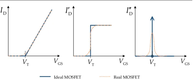
After reviewing several methods [27] it is selected the second derivative method [28], which offers an extraction ofVTwith relatively easy procedure and ensures an indepen-dence from series resistances. This last point is very important, especially in TFTs that can have contact resistances in theMΩlevel.
The idea behind this method comes from the concept of an ideal MOSFET in linear region, where the currentID= 0 forVGS< VTand forVGS> VTthe currentIDis directly proportional toVGS. The first derivative
dID
dVGS
results into a step function that remains zero forVGS< VT, and produces a positive constant value forVGS> VT. Thus, the second derivativedVd2ID2
GS
results into a Dirac delta function which in this case, is zero for all values except forVGS=VT, here function tends to∞. For a real device such simplification is not totally correct, instead of the function becoming∞atVGS=VT, it exhibits a maximum at this value.
In Fig. 3.1 it is illustrated this mathematical behaviour in both real and ideal FET.
C H A P T E R 3 . A B OV E -T H R E S H O L D PA R A M E T E R E X T R AC T I O N A N D L I N E A R M O D E L
T
V
V
GSD
I
T
V
V
GST
V
V
GSD
I
D
I
Ideal MOSFET Real MOSFET
Figure 3.1: Second derivative method forVTextraction in real and Ideal FET.
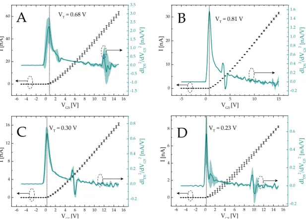
3.1.1 Results
After using the 2nd derivative method for the devices in study and smoothing out the data with OriginLAB (the Savitzky-Golay smoothing method is chosen to preserve the spike nature atVT), it was obtained the following Fig.3.2. The extracted values ofVTcan be found in Tab. 3.1.
Table 3.1: ExtractedVTvalues for different channel lengths
L(µm) VT(V)
20 0.68
40 0.81
80 0.30
160 0.23
The second derivative method can be quite noisy, this is mainly due to how the soft-ware does the derivative. Here the derivative is done by differentiating point by point, thus it is highly sensitive to small measurement changes. Regardless of that, the spike atVT is very clear. In terms of the actual value ofVT, we observe a relatively large dis-crepancy for the different Ls (worst case has 0.58 V difference), this may present as a problem for the model. As a circuit designer perceptive you seek for a model that has standard parameters which can be trustworthy for any given transistor dimensions in that particular technology, otherwise the forecast ability of that model in circuit design is jeopardised.
3.2 Contact resistance,
R
DSW
and
∆
L
TFT devices are structured with several different materials, in this regard the interface between them produces a high resistance (when compared with MOSFET). The contact resistanceRDShappens at the interface between the active layer (IGZO) and source/drain
3 . 2 . CO N TAC T R E S I S TA N C E ,RDSW A N D∆L
-6 -4 -2 0 2 4 6 8 10 12 14 16 0
20 40 60
-5 0 5 10 15
0 10 20 30
-6 -4 -2 0 2 4 6 8 10 12 14 16 0
4 8 12 16
-6 -4 -2 0 2 4 6 8 10 12 14 16 0 2 4 6 8
D
C
B
VT = 0.81 VI [
nA
]
VGS [V]
VT = 0.68 V
A
-1.5 -1.0 -0.5 0.0 0.5 1.0 1.5 2.0 2.5 3.0 3.5 dlD S 2 /dVGS
2 [n
A /V ] I [ nA ]
VGS [V]
-0.2 0.0 0.2 0.4 0.6 0.8 1.0 1.2 1.4 1.6 dlD S 2 /d
VGS
2 [n
A
/V
]
VT = 0.30 V
I [
nA
]
VGS [V]
-0.2 0.0 0.2 0.4 0.6 0.8 dlD S 2 /d
VGS
2 [n
A
/V
]
VT = 0.23 V
I [
nA
]
VGS [V]
-0.2 0.0 0.2 0.4 0.6 dlD S 2/d
VGS
2 [n
A
/V
]
Figure 3.2: Extracted values ofVT for TFT devices withW ∼20µm. The black plot is
forIDS(VGS) characteristics, while the blue plot is the second derivative of the black plot. The error bar comes from the three replicas measured. A) L∼20µm; B)L∼40µm; C)
L∼80µm; D)L∼160µm.
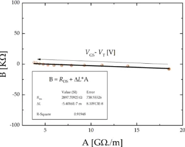
sides respectively. In order to findRDS, the Eq. (2.6) is solved in order of total measured resistance,RT
RT =VDS
IDS =RDSW+
L+∆L
K(VGS−VT)a−1 (3.1)
whereL+∆LisLeff(effective channel length may differ from the masked due to fabrication
process). According to (3.1), if one plotsRT versusLfor variousVGS−VT*, the intercept point should give∆LandRDS[29]. However in practice the intercept never happens in
a single point, so a more accurate method is to use the slope (eg. A) and the y-intercept (eg. B) to create a new plotBversusA[30]. In this new plot the slope will give∆Land
the y-intercept theRDS. The rewritten equation for 3.1, in respect toAandBis as follow:
B=RDS+A∆L
A= 1
KW(VGS−VT)α−1
(3.2)
An illustrative procedure of these stages can be found in Appendix A
*The normalization of voltages is very important for good parameter extraction, especially after the discrepancy observed in Tab. 3.1.
C H A P T E R 3 . A B OV E -T H R E S H O L D PA R A M E T E R E X T R AC T I O N A N D L I N E A R M O D E L
3.2.1 Results
The intermediate plots ofRT vsVGS−VTandRT vsLcan be found in Appendix B. The plot ofBvsAis presented in Fig. 3.3 and the extracted values can be seen in Tab. 3.2.
Figure 3.3: BvsAplot forRDSand∆Lextraction
Table 3.2: Extracted values forRDSW and∆L
RDSW (Ωcm) ∆L(µm)
5.794±1.4770 −0.54±0.08
For general purposes value ofRDSis multiplied withW. By comparing this value with other TFT devices with similar structure [26, 31] (values forRDSW from few hundred Ωcm to several kΩcm ), we can say that the contact resistance is quite low, this fact will
come in handy for later parameter extraction.
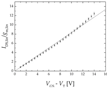
3.3 Power parameter,
α
The power parameterαcan be extracted by dividingIDS,lin(2.6) with its first derivative (gm,lin) as follow:
IDS,lin gm,lin =
VGS−VT−0.5VDS α−1
VDS
VDS−RDSIDS,lin (3.3)
From Fig. 3.2 the current in linear region is at nA level andRDS(@W ∼20µm) is a few kΩ, therefore the voltage produced byRDSIDS,lin is around theµV level. Thus the
RDSIDS,linis much smaller thanVDS(5 mV). Apart from that, by comparingVDSwith the
3 . 4 . T R A N S CO N D U C TA N C E PA R A M E T E R ,K
other two voltages of Eq. 3.3 we can neglectVDS. The final simplification is as follow:
IDS,lin gm,lin =
VGS−VT
α−1 (3.4)
The slope of IDS,lin
gm,lin vs (VGS−VT) can be used to extractα. The result of the plot of Eq. 3.4
is presented in Fig. 3.4
Figure 3.4: IDS,lin
gm,lin vs (VGS−VT) for alpha extraction (R
2= 0.998).
The linear fitting is done in such way that forces the intersect at (0,0), even with this theR2= 0.998 so a good extraction ofαis achieved (α= 2.2).
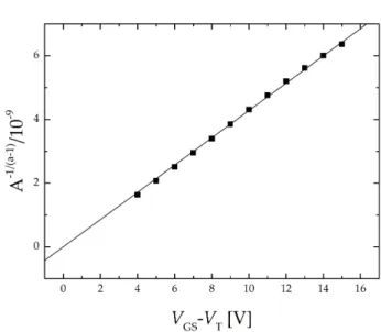
3.4 transconductance parameter,
K
Since we have all other parameters for the model,Kshould be straight forward to obtain. A plot ofA−1/(a−1) vsV
GS−VT may be used to extractK. This method is analogous to
√
IDS/W vsVGSfor mobility extraction in MOSFETs.
Sa−1=KW (3.5)
WhereS is slope of the best linear fit. The plottedA−1/(a−1) vsVGS−VT graph may be found in Fig.3.5 The extracted value forKis 5.2×10⁻⁷.
3.5 Model representation
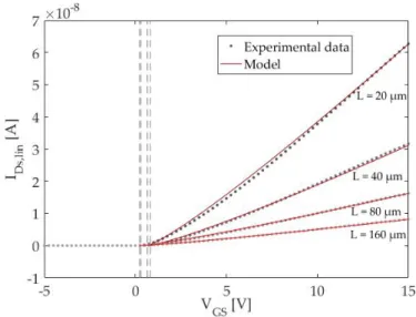
After all the exhausting work of parameter extraction, we final arrive to the exciting part of model representation. Recalling the Eq. (2.5)
IDS,lin=K W Leff
"
VGS−VT−IDSRDS2
α−1 (V∗
DS−IDSRDS)−
1−1 α
(V∗
DS−IDSRDS)α #
C H A P T E R 3 . A B OV E -T H R E S H O L D PA R A M E T E R E X T R AC T I O N A N D L I N E A R M O D E L
Figure 3.5:A−1/(a−1)vsVGS−VTplot forKparameter extraction
and with the parameters extracted throughout this work (summarized in Tab. 3.3). The above threshold linear model is obtained with the resource of MATLAB as in Fig. 3.6.
Table 3.3: Summary of all parameters extracted for above-threshold linear model
L(µm) VT(V) RDSW (Ωcm) ∆L(µm) α K
20 0.68
5.794 -0.54 2.2 5.2×10⁻⁷
40 0.81
80 0.3
160 0.3
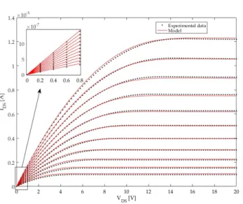
In order to be able to represent the output characteristics, some sort of saturation model is required, in this case the following is considered:
VDS∗ =hVDS−m+ (VGS−VT)−mi−
1
m (3.6)
If we now letmbe positive, then forVDS ≫VGS−VTthe Eq. 3.6 will be dominated by
theVGS−VT, in the other hand whenVDS≪VGS−VTthe same equation will tend toVDS. This constantmis defined empirically, withm= 6 the following output characteristics is obtained for different size transistors Fig. 3.7 and Fig. 3.8.
3.5.1 Discussion of Results
Analysing the results of the modelled I-V, and comparing it to the measured devices, one could say that the overall model is good to predict the behaviour of the TFT devices in study (r2= 0.97 for linear region). However this is done at the cost of having measured theVTof every different size of transistor. Alongside that no apparent pattern is observed to enable the forecast ability ofVTwithout changing the fundamental model. Moreover
3 . 5 . M O D E L R E P R E S E N TAT I O N
Figure 3.6: Comparison between theIDSvsVGScharacteristics for the measured devices and developed model based on Eq. (2.5). TheVDS is maintained at 5 mV, to ensure the linear region
Figure 3.7: Output characteristics forL∼20µm andW ∼20µm.
C H A P T E R 3 . A B OV E -T H R E S H O L D PA R A M E T E R E X T R AC T I O N A N D L I N E A R M O D E L
Figure 3.8: Output characteristics forL∼160µm andW ∼20µm.
the equation of the model has only numerical solution, if no simplifications are assumed. Therefore solving these equations can take long time for each transistor. Restricting the use of this model for only simple circuit simulations. Regardless of that, this is already a good milestone.
Focusing on the output curves, the harmonic averaging method is quite good to make a smooth transition between the conventional linear and saturation regions. This avoids any convergence problems between these regimes. Nonetheless for this method to work themvalue has to be attained empirically.
In many cases circuit designer like to do a simple and quick analysis (eg. DC operating point) in such scenarios it is interesting to have a simple separate saturation equation. A good option would be would be to consider the following equation:
IDS,sat=cK α
W L
VGS′ −VTα (3.7)
wherechad to be attained from fitting. The same harmonic averaging could be used for the transition between regions. However even with this we might not safeguard a smooth behaviour.
4
Small-signal model
From earlier chapter 1.4.1 we have seen that a generic three terminal device transistor can be represented with the hybrid-pi model. Moreover, the small signal model of the MOSFET that is adapted for TFT at low frequency is shown in Fig. 4.1. Here it is assumed based on the previous study, that the contact resistance is low enough hence it may be neglected. m gs
g v
S
D
G
gsv
+
-or
Figure 4.1: Low frequency small signal MOSFET model adapted for TFT
4.1 High Frequency TFT model
With the rise of the frequency of a given small AC signal, the whole TFT device physics has to be reconsidered especially with parasitic capacitances, that now start to shine.
The Bottom-Gate TFT structure is usually designed to ensure some overlap in the source electrode and Drain electrode as a misalignment margin for the lack of precision during lithography processes. Without this margin any unwanted offset may result in orders of magnitude reduction in IDS. The downside of this overlap is the parasitic capacitance that forms in both source (CS) and drain (CD) electrodes.
Besides these parasitic capacitances there is the channel capacitanceCch that forms between the gate and active layer. With these parasitic components in mind the model for small signal at high frequencies becomes the one shown in Fig. 4.2.
With this structure in mind and in order to evaluate the capability of this model to represent the devices in study, the relationship between input and output current is studied. This allows the calculation of current gain at short circuit (Ai).
Ai=iiout
in (4.1)
Whereioutandiinare defined as
iin=vinsCD+ (vin−vout)sCS+ch iout=voutgo+vingm+ (vout−vin)sCS+ch
(4.2)
C H A P T E R 4 . S M A L L- S I G N A L M O D E L
S+ch
C
D
C
m gs
g v
S
D
G
o
r
Figure 4.2: High frequency small signal MOSFET model adapted for TFT.
Substituiting Eq. (4.2) in Eq. (4.1) and consideringvout= 0 we get the current gain for the MOSFET model adapted to TFT as follow:
Ai=s(Cgm−sCD
D+CS+ch) (4.3)
From equation Eq. (4.3) it is possible to extract that the model has one pole (at 0 Hz) and one zero (at CDgm Hz). If one considers that the zero is far from the cut-offfrequency then the unit-gain frequency is given by:
fT= gm
2π(CD+CS+ch) (4.4)
4.1.1 Measurement setup
From the previous section, in order to build an AC model it is necessary to measure the current gain of the real device and compare the unit-gain frequency to evaluate the good-ness of the model. One of the most common way to quantify this frequency is through a network analyser which can measures-parameters, furthermore these parameters are useful for the calculation ofh-parameters. More specifically theh21value gives the short-circuit current gain (Ai).
For the purpose of these measurements, a Keysight E5061B network analyser (ENA) is used which is calibrated with CS-11 calibration substrate provided by GGB Industries, Inc. The standard measurement set-up is shown in Fig. 4.3. The bias-T separates the small signal input and output form the DC biasing circuitry.
This analyser is chosen due to its low frequency measurement capability (down to 5 Hz). In contrast, conventional network analysers work in the 100 kHz range, which may already be in the cut-offfrequency level of the TFTs.
The ENA in use is capable of providing both DC and bias-T at port 1. However for port 2 an external bias-T is required. Since it is necessary to measure low frequencies (in comparison to MOSFET), the Picosecond 5546 bias-T is used which offers 3.5 kHz as per the low 3 dB frequency (lowest found on the market).
4 . 1 . H I G H F R E Q U E N C Y T F T M O D E L
Bias-T
ENA Port 1
(with DC bias and bias-T)
Probe Station
DC bias
ENA Port 2
Figure 4.3: Measurement set-up for s-parameters andfT.
The bias conditions are chosen to beVGS= 8V andVDS = 15V to ensure saturation regime. The devices used haveW /L ratio of 160µm/20 µm and 320 µm/20 µm, it is chosen large channel width mainly for an accurate capacitance extraction. In the same way that there is a variation of the channel length there is also a variation of channel width, at larger values ofW this contribution is neglectable. The smaller channel length is chosen for a faster measurement, and it was the only fixedLvalue with differentWs available in the sample.
A calibration process is conducted by the aforementioned substrate and the Picoprobe Model 10 by GGB Industries, Inc. This calibration is essential to cancel out any parasitic effect from the setup (wires, probes etc.) for S-Parameter measurements.
4.1.2 Dominants-parameters for measurement and analysis
Before starting any measurements ofs-parameters it is important to analyse the expres-sion ofh21in function to thes-parameters for a network of two-ports [32].
h21=− 2S21
√
R01R02
(1−S11)(Z02∗ +S22Z02) + (S12S21Z02) (4.5)
Where,Z01andZ02are the normalizing impedance of source and load respectively, in whichs-parameters are calculated or measured;∗representes the complex conjugate ofZ; finalyR01andR02represent the real part ofZ01andZ02respectively.
Since in both source and load sides the normalized impedance that is used is 50Ω
(pure real impedance), the Eq. (4.5) simplifies into:
h21=−(1 2S21
−S11)(1 +S22) + (S12S21) (4.6)
To further simplify Eq. (4.6) it is necessary to understand how eachs-parameter will contribute in the equation. In Fig. 4.4 it is shown the equivalent circuit to measureS11 andS21; forS22andS12it is just necessary to change the position ofZ0from one port to another.
C H A P T E R 4 . S M A L L- S I G N A L M O D E L o
r
S chC
DC
m gsg v
1a
a
21
b
b
2in
v
in
i
i
outout
v
Two-port network
Port 1
Port 2
21
S
11S
12S
22S
LZ
0Z
Figure 4.4: Equivalent circuit forS11andS21measurements.
Thea1anda2represent the normalized incedent voltages, andb1andb2the normal-ized reflected voltages, these are defined as
a1 a2
b1 b2 =
Vin+Z0Iin
2√Z0
Vout+Z0(−Iout) 2√Z0 Vin−Z0Iin
2√Z0
Vout−Z0(−Iout) 2√Z0
(4.7)
Thes-parameters matrix in respect to the normalized voltages is given by
S=
S11 S12 S21 S22 = b1 a1 a2=0 b1 a2 a1=0 b2 a1 a2=0 b2 a2 a1=0 (4.8)
Using Eq. (4.7) in Eq. (4.8) it is possible to solve S11 andS22 with only terms of impedance, whereZLis the correspondent impedance forSxx(S11;S22).
Sxx= ZLZL−+Z0Z0 (4.9)
From the earlier DC model, if we analyse Fig. 3.7 and Fig. 3.8 it is possible to say that the TFTs on study are very resistive devices when compared to MOSFET, and this is also true for the general case of TFTs. As TFTs are normally biased from a few volts to 20 V this will generate currents of a fewµA (at saturation), which corresponds to 100 kΩor even MΩlevel resistances. This fact results inS11andS22 values to be near 1, asZLis much larger thenZ0.
One could argue that at higher frequencies the impedance of the capacitive elements will drop drastically, however for the frequency range of concern, that is before the cut-off frequency, this effect is not so drastic and so the assumption (ZL≫Z0) remains correct for the working frequency range.
As illustrated in Fig. 4.4, theS11andS22represent the ratios between the reflected and incident electromagnetic power wave, for their respective ports. Since these reflection coefficients are near to 1, most of the energy from the wave is reflected back rather then transmitted from one port to another. Thus, the transmission coefficients given byS21 andS12must be close to 0.
4 . 2 . S- PA R A M E T E R S
With thes-parameters briefly analysed we can now go back to Eq. (4.6) and try to see how the weight of each parameter will influence. The major complexity comes from the denominator since both terms (1−S11)(1 +S22) andS12S21are close to 0. To try to find out which one is more relevant it is done the following:
T1= (1−(1−∆11))·(1 + (1−∆22)) T2=∆12∆21
Where∆represent a quantity that is close to 0. If now one assumes that the different
∆s are all the same then the terms simplify into:
T1= 2∆−∆2
T2=∆2
(4.10)
From here it is possible to conclude that the first term of the denominator will dominate over the second (2∆≫∆2). Hence, another observation that can be done is (1 +S22)≈2
and so the final simplification for Eq. (4.6) is
|h21| ≈
S21 (1−S11)
(4.11)
This demonstrates that most relevants-parameters for TFT modelling areS21andS11.
4.2
S
-Parameters
In this section it is analysedS11andS21.
4.2.1 S11theoretical analysis
First, it is necessary to calculate the theoretical expression that givesS11for the CMOS model adapted to TFT. This is easily achieved through Eq. (4.9), where the most com-plicated part is findingZL. For this it is considered the following circuit present in Fig. 4.5
o
r
Z
0S+ch
C
DC
m gsg v
xv
xi
av
0Z
Figure 4.5: Equivalent circuit to obtainZLforS11expression.
By applying Kirchhoff’s current law (KCL) to the nodesxanda, we get the following equations
C H A P T E R 4 . S M A L L- S I G N A L M O D E L
ix=vx(sCS+ch) + (vx−va)sCD (vx−va)sCD=gmvx+g0va
(4.12)
Here the equations are written in terms of conductance to visually look simpler, fur-thermore it is done an approximation forro//Z0toZ0. This is particularly possible in the TFT case, where the device is naturally very resistive. For example, the drain output resis-tance (ro)*is ideally∞and for the real device is on the MΩlevel. In the other spectrum Z0is just 50Ω, and therefore the conductanceg0dominates over 1/ro.
Now, by solving Eq. (4.12) in respect tovx
ix =ZLwe get
ZL= "
sCS+ch+sCD+sCD(gm−sCD) g0+sCD
#−1
(4.13)
Finally, by substituting Eq. (4.13) in Eq. (4.9) we get the expression ofS11for the CMOS model adapted to TFT.
S11=− −go
2+CS+chgos+CS+chCDs2+CDgms
go2+CS+chgos+CDgms+ 2CDgos+CS+chCDs2 (4.14)
4.2.2 S21theoretical analysis
In order to figure out the equation that describes theS21for the MOSFET model adapted to TFT, it is considered the Eq. (4.7) and Eq. (4.8). From here we get the following
S21= b2 a1 =
Vout−(−IoutZ0)
Vin+IinZ0 =
2Vout
Iin(ZL+Z0) (4.15)
By looking at this result, one can notice that the difficult part is to express the quotient ofVout/Iin, sinceZLis already determined in Eq. (4.13). Observing the Eq. system (4.12), the second equation can be solved in order tovawhich is the same asVoutandvx=Vin.
Vout=Vin·sCDg −gm
0+sCD (4.16)
Now, by dividing both terms withIinwe get the following
Vout Iin =ZL·
sCD−gm
g0+sCD (4.17)
Finally, by substituting Eq. (4.17) in Eq. (4.15) with the result forZLfrom Eq. (4.13), we have
S21=− 2go(gm−CDs)
go2+CS+chgos+CDgms+ 2CDgos+CS+chCDs2 (4.18)
*this is given by the operation of the transistor in the saturation region and it should not to be confused with the channel resistance, which is a different thing [33]
4 . 3 . M O D E L VA L I DAT I O N
4.3 Model validation
4.3.1 Pre requirements
In order to attain the theoretical values of the s-parameters it is necessary to measure some variables. Analysing (4.14) and (4.18), we find thatCS+ch,CDandgmare still unknown.
For the first two, C-V measurement are done in Keithley 4200. It is considered the same transistors with W/L ratios of 160µm/20µm and 320µm/20µm, for later com-parison purpose. A capacitance-voltage unit (CVU) voltage sweep is performed from -1 V to 10 V with 0.1 V increments, the frequency used is 10 kHz and a small AC signal is applied of 30 mV. The C-V characteristics for one of the devices can be found in Fig. 4.6.
C 2 / 3
ch
2 / 3C
Figure 4.6: C-V characteristics for 320µm/20µm TFT
If we now Consider a symmetrical device both overlap capacitance will equal so:
CS=CD=Clow2 (4.19)
After the pitch-offcondition (at saturation) the channel capacitance is given by:
2 3Cch=
Chigh−Clow
(4.20)
With the capacitance determined it was time to find the value forgm. This value can be found from the first derivative ofdVGSdID at saturation condition. Another alternative much efficient and used in this project, is to considering equation 4.18. At very low frequency it will simplify into:
lim
s→0S21=− 2gm
g0 (4.21)
The values obtained for the devices in study for this section is summarized in Tab. 4.1.
C H A P T E R 4 . S M A L L- S I G N A L M O D E L
Table 4.1: Extracted values for s-parameters representation
Transistor (W /L) CS(F) Cch(F) gmΩ−1
320/20 4.91×10⁻¹³ 2.92×10⁻¹² 8.91×10⁻⁵ 160/20 3.82×10⁻¹³ 1.14×10⁻¹² 4.55×10⁻⁵
From the observation of this table, the overlap capacitance (CS) between the smaller and the larger device is not proportional to 0.5. If we discard the channel width variations, one possible explanation could be attributed to the ratio of overlap between drain/gate or source/gate which must be higher at the smaller device leading to a higher overlap capacitance.
4.3.2 Model representation
Having all relevant s-parameters measured and obtained the values for their representa-tion. It was finally possible to compare both.
Starting with S11, the following Fig.4.7 is obtained for the transistor with W /L = 160/20. Due to similar behaviour the other device is presented on Appendix C.
(a) Magnitude (b) Phase
Figure 4.7: Magnitude and phase measurement and simulation forS11for TFT with W/L= 160/20.
From 4.14, it is suggested that the model has 2 zeros and 2 poles. From the calculation of both it was obtained 2 zeros at−6.2×10¹⁰Hz and−6.2×10¹⁰Hz; 2 poles at−6.6×10¹⁰ Hz and−9.1×10¹⁰Hz. As zeros and poles are very far from the range of frequency of concern, the modelled value forS11make sense in remaining at 0 dB. Since the measured S11drops much earlier it suggests either the poles and zeros happen earlier or there has to be an extra pole and zero at earlier frequencies.
The next parameter for comparison isS21(Fig. 4.8).
From the analytical expression forS21Eq. (4.18), the model suggest to have 2 poles and 1 zero. The calculations point that the poles are located at−6.6×10¹⁰Hz and−9.0×10⁹
![Figure 1.1: Small-signal model for a general 3 terminal device in mid-band frequency, also known as hybrid-pi model [12].](https://thumb-eu.123doks.com/thumbv2/123dok_br/16693495.743729/27.892.213.637.764.995/figure-small-signal-general-terminal-device-frequency-hybrid.webp)