iii
"Podem ser encontrados aspetos positivos até nas situações
negativas e é possível utilizar tudo isso como experiência para o futuro,
seja como piloto, seja como homem."
v
A
CKNOWLEDGEMENTS
I want to acknowledge Professor José Carlos Teixeira and Professor Sérgio Sousa,
my supervisors, for all the help, support and orientation during this year.
Special thanks to Bosch Car Multimedia for the opportunity to make this work there and
to Luís Ribas to help me with all my questions and doubts.
For all the motivation and opportunity to carry out this thesis I must thank to my
mother, sisters and brother in law for all the patience they have with me and for all of the sacrifices
they made so I could get here.
To my aunt Sylvie who always was there for me and gave me strength to finish this stage.
To my boyfriend for all the support and to believe that I would get there.
vii
A
BSTRACT
To overcome the production peak and the sudden production volumes demand is
necessary to look for others factories outside the Bosch Car Multimedia (CM) to achieve the sales
target.
The components assembly on a printed circuit board (PCB) involves several important
factors that can influence the products final quality and also compromise the Bosch CM quality.
The different processes used in the assembly of the PCB can be crucial to the quality and for that
they should be well studied and identified to prevent mistakes and prevent that defective products
reach the client.
The aim of this work is to characterize the PCB assembly line processes and also define
the most important proprieties of each process that must be followed to guarantee that the Bosch
CM quality is fulfilled.
Thus is made the study of all the processes that are part of the production line and are
collected the most important characteristics of each process that can influence the final quality of
the products and put the Bosch CM name in cause. This collection was compiled in the
“Outsourced Process and Extended Workbenches of Electronic Assemblies” (Appendix I). This
document, with the help of a Technical Assessment Checklist (Appendix II) that was made based
on this and must be fully implemented, will ensure that the Bosch CM quality is maintained during
the manufacturing of this products.
The results obtained will help the implementation of new production lines outside Bosch
CM, helping the growing demand of the products, the compliance of the dead lines without
forgetting the product quality that required by the client.
ix
R
ESUMO
Para superar os picos de produção e ainda a procura repentina de grandes volumes de
produção faz com que seja necessário procurar outras fábricas fora da Bosch Car Multimédia para
alcançar as metas de vendas dos produtos.
A montagem dos componentes numa placa de circuito impresso (PCI) envolve vários
fatores importantes que podem afetar a qualidade final do produto e ainda por em causa a
qualidade de produção da fábrica. Os diferentes processos usados na montagem dos
componentes nos PCI podem ser decisivos na qualidade final dos produtos e por isso devem ser
bem estudados e identificados para evitar erros nos produtos finais e evitar que estes produtos
defeituosos cheguem até ao cliente.
Assim, nesta dissertação pretende caracterizar-se os processos usados pela Bosch CM na
montagem dos componentes nos PCI e ainda determinar as propriedades mais importantes de
cada processo que devem ser seguidas para que a qualidade usada pela Bosch CM não seja
descurada.
Desta forma é feito o estudo processo a processo que constituem uma linha de produção
e são recolhidas as características mais importantes de cada processo que possam afetar a
qualidade final dos produtos e colocar em causa o nome e reconhecimento da Bosch CM. Esta
recolha foi então compilada no documento “Outsourced Process and Extended Workbenches of
Electronic Assemblies” (Anexo I). Este documento, com ajuda de uma lista de requisitos (Anexo II)
feitos com base neste e que deve ser totalmente cumprida, vai garantir que a qualidade da Bosch
CM é mantida enquanto estes produtos são fabricados.
x
Os resultados obtidos irão ajudar à implementação de novas linhas de produção fora da
Bosch Car Multimédia ajudando assim a procura crescente de produtos, o cumprimento dos
prazos de entrega sem descurar a qualidade que o cliente exige para os seus produtos.
xi
T
ABLE OF
C
ONTENTS
Acknowledgements ... v
Abstract ... vii
Resumo ... ix
Table of Contents ... xi
List of Figures ... xiv
List of Tables ... xvi
List of Abbreviations ... xvii
CHAPTER 1
Introduction ...1
1.1
Motivation ...2
1.2
Objectives ...3
1.3
Structure ...3
CHAPTER 2
Literature Review ...5
2.1
History of the Printed Circuit Board ...5
2.2
PCB’s Fabrication ...6
2.3
PCB Assembly Line Evolution ...9
2.4
Bosch Production System (BPS) ...11
CHAPTER 3
PCB Assembly Line ...13
3.1
PCBA in the BOSCH CM ...13
3.2
General Requirements for the production line ...14
3.3
PCB Handling ...17
3.4
PCB Laser Marking ...18
xii
3.6
Solder Paste Printing ... 19
3.7
SPI – Solder Paste Inspection ... 21
3.8
SMT – Placement ... 22
3.9
Automatic Optical Inspection (AOI) ... 22
3.10
Through-hole Technology ... 23
3.11
Adhesive Dispensing and Curing ... 24
3.12
Soldering ... 27
3.12.1
Reflow ... 27
3.12.2
Wave Soldering ... 29
3.12.3
Selective Soldering ... 30
3.13
X-Ray ... 31
CHAPTER 4
Presentation and discussion of the results ... 33
4.1
Outsourced Process and Extended Workbenches of Electronic Assemblies ... 34
4.2
Technical Assessment Checklist ... 36
4.3
Solder Paste Printing ... 38
4.3.1
Environment ... 41
4.3.2
Storage... 41
4.3.3
Materials ... 43
4.3.4
Tools ... 45
4.3.5
Cleaning ... 46
4.3.6
Maintenance ... 47
4.3.7
Process Control ... 47
4.3.8
Machine Capability ... 47
4.3.9
Process Capability ... 48
xiii
4.4
Conclusions ...49
CHAPTER 5
Conclusions and future work ...51
5.1
Future Work ...52
References ...53
Appendix I – Outsourced Process and Extended Workbenches of Electronic Assemblies ...59
Appendix II – Technical Assessment Checklist ... 167
xiv
L
IST OF
F
IGURES
Figure 1- PCB example [3] ... 7
Figure 2- PCB with 2 Layers ... 7
Figure 3 - Fiberglass-resin laminate (FR4) [5] ... 8
Figure 4 – Pads [6]... 9
Figure 5 - PCB with soldermask and silkscreen [7] ... 9
Figure 6 - History of Lean Production ... 10
Figure 7 - Bosch Business System (BBS) ... 11
Figure 8 - PCBA line (side A) ... 13
Figure 9 - PCBA line (radial insertion and side B) ... 14
Figure 10 - Examples of ESD logo ... 15
Figure 11 - MSD Dry Bag [12] ... 16
Figure 12 - Humidity indicator and Desiccant [12] ... 16
Figure 13 - Allowable PCB warpage ... 17
Figure 14 - 1D Barcode... 18
Figure 15 - 2D Data Matrix Code [14]... 19
Figure 16 - Human readable text [14] ... 19
Figure 17 - Common Surface Mount Devices [21] ... 22
xv
Figure 19 - Axial components insertion [22]... 24
Figure 20 - Radial Insertion ... 24
Figure 21 - Pressure System (Adapted) [23] ... 25
Figure 22 - Auger Pump System (Adapted) [23] ... 26
Figure 23 - System Pump System (Adapted) [23] ... 26
Figure 24 – General Solder Convection Reflow Solder Profile [25] ... 28
Figure 25- Wave Soldering Scheme (Adapted) [28] ... 30
Figure 26 - X-Ray inspection of BGA [29] ... 31
Figure 27 - Static X-Ray Scheme [31] ... 32
Figure 28 – Technical Assessment Checklist example sheet [appendix III] ... 36
Figure 29 – Technical Assessment Checklist example of Solder Paste Printing Process ... 37
Figure 30 – Stages of the evaluation ... 37
Figure 31 - Ratting Grade ... 38
Figure 32 - Defect Chart for All Electronics Assemblies ... 39
Figure 33 - Defect Chart for SMT (only) Assemblies ... 39
Figure 34 - Common used Fiducials [34] ... 40
Figure 35 - Usage Timeline for Solder Paste ... 42
Figure 36 - Amount of solder paste on the Stencil ... 43
Figure 37 - Step Up Stencil [37] ... 45
Figure 38 – Stencil Step up scheme ... 45
xvi
L
IST OF
T
ABLES
Table 1- Bosch Production System Principles ... 12
Table 2 - Figure 5 caption ... 13
Table 3 - Figure 6 Caption... 14
Table 4 - Minimum and Maximum Allowable Temperature and Humidity ... 41
Table 5 - Heraeus F620 Specifications ... 41
Table 6 - Stencil Surface Treatment... 44
Table 7 - Stencil Lifetime... 44
Table 8 - Specification limits for 150 µm stencil ... 48
Table 9 - Specification limits for 125 µm stencil ... 48
xvii
L
IST OF
A
BBREVIATIONS
CM – Car Multimedia
EPA – Electrostatic Protected Area
ESD – Electrostatic Safety Discharge
HIC – Humidity Indicator Cards
MSD – Moisture Sensitive Device
PCB – Printed Circuit Board
PCBA – Printed Circuit Board Assembly
SJI – Solder Joint Inspection
SPI – Solder Paste Inspection
SMD – Surface Mount Device
SMT – Surface Mount Technology
THT – Through-hole technology
UV – Ultraviolet light (400 – 10nm wavelength)
UVA – Ultraviolet light
1
CHAPTER 1 I
NTRODUCTION
Printed Circuit Boards (PCBs) are strongly used in the electronic industry. They are used
in devices like navigation systems, cell phones, radios, etc.
These boards can be made of one or more layers and the components are mounted in the
surfaces of the board.
One of the most important factors in the assembly of the PCB is the way that the
components are mounted on the board and the way that the production line and the production
line parameters are defined.
With the decrease of the size of the PCB’s, the consequent decrease of the components
and the increasing of the number of components per PCB the production and the mounting of the
PCBA had also to evolve.
Therefore, in this context, together with Bosch Car Multimedia, it was developed the project
“PCBA External Workbench Evaluation Procedure”. The aim of this work is to identify and
characterize failures that may happen during the PCB assembly. These failures can result in a
defective PCB and latter to a malfunctioning device. This document need to be implemented in
the PCB assembly line and for that it was developed a checklist that will help and facilitate the
implementation of this rules at the new line.
With this work and with the use of the developed checklist it will be easier the evaluation
and characterisation of the assembly line and above all guarantee that this line fulfils the Bosch
requirements.
2
1.1 Motivation
Market competitiveness has led companies to develop new products more frequently,
resulting in small quantities per product and bigger product variety. This, together with increased
product complexity, puts pressure in quality activities. The quality level in the automotive industry
is measured in parts per million (PPM) of defective units. The way to achieve such levels of
performance is typically based on preventive actions, supported by self-assessment activities, and
the standardization of tasks, specially the manufacturing ones.
To fulfil strategic decisions and to respond to market demand variations, companies often
subcontract new suppliers to provide not only raw materials and components but also to execute
some of its core manufacturing processes.
To accelerate the productive process without forget the quality it was necessary to adopt
some measurements like the standardization of the production. With the standardization it was
easier to improve the technical level of the employees and guarantee that the production
parameters are always the same whether the production is made now or with weeks apart. The
final product has always to have the same characteristics.
With the standardization and the development of the techniques used will enable the
reduction of the consumption and scrap. The equipment used will be standardized and the
production will increase as also the quality. The process is also controlled with the improvement of
these two techniques.
For this reasons and to help the implementation of new production lines outside the Bosch
Car Multimedia factory was developed this work. The development of the checklist that will
guarantee that the production line hired fulfils all the Bosch requirements and all the client
specifications became an important challenge for me.
3
1.2 Objectives
The aims of this work are:
Develop a system to define the requirements which the PCBA providers will have
to fulfil in order that the final product has the same quality as if an in-house production
was;
Contribute to Decrease PCB defects and scrap;
Implement a technical checklist that defines the necessary requirements for the
implementation of PCBA in another factory;
Improve and accelerate the approval of new external PCBA suppliers that fulfil
BOSCH requirements.
1.3 Structure
This work is structured in five chapters. Thus, after the introduction of the theme, the
second chapter presents literature review about the history of the printed circuit board, the PCB’s
fabrication and also the history of the PCB assembly line evolution that introduces methodology
used by Bosch CM, the Bosch Production System (BPS).
In the third chapter is characterized the Printed Circuit Board assembly line used in Bosch
Car Multimedia. This chapter is divided in twelve sections that characterize all the most important
phases of the assembly process for both PCB line side A and B.
In chapter four is made the presentation and discussion of the results. This chapters is
divided in four sections. In the first one is characterized the “Outsourced Process and Extended
Workbenches of Electronic Assemblies” and in the second one the “Technical Assessment
Checklist” that are the base of this work. In the third section is presented one of the most important
processes of all line, the Solder Paste Printing process, that can influence the all line if is not well
done. In sub-chapter four are presented the conclusions retained of this results.
To finalize, in chapter five, are presented the main conclusions taken by this work and the
future work to be done.
5
CHAPTER 2 L
ITERATURE
R
EVIEW
In this chapter is made the review of the state of the art. Firstly is made a review of the
Printed Circuit Board history, from the first PCB to the present day and is also made a brief resume
of the fabrication of the PCB’s and its composition. Finally is characterized the line flow in the
timeline.
2.1 History of the Printed Circuit Board
If we look around us we notice the amount of electronic devices surrounds us and which
are integral part of our life. All of these devices are constituted by PCB’s and electronic components.
The PCB’s are being developed by years and, according Joseph Fjelstad [1] , the electrical systems
used in 1850s gave rise to the PCBs. Later the metal stripes used to connect large electrical
components were replaced by wires connected to terminals and the wood base by metallic
structures. In 1904, Sprague and is mentor Thomas Edison, want to replace the point-to-point
wiring and tested methods of using metals in linen paper.
Later in 1925, was developed by Charles Ducas [2] a method that uses electroplating with
an electrical path using a stencil and a special paint that could conduct electricity.
Paul Eisler has patented a method to print a circuit board above one layer of cooper in a
strong base that couldn’t conduct the electricity.
Was in the end of the World War II that the U.S National Bureau of Standards (NBS)
developed a technic used by the U.S army more similar with the actual printed circuit board. This
technic consisted in printing silver paste conductors and graphite resistors onto ceramic substrates.
This technic marked the begin of the commercial use of PCBs.
6
The search for consumption products after the World War II has increased and some new
technics were explored during the years. When the PCB has reached the maximum density the
single sided boards were substituted by double sided boards. The multilayer appear in 1956 to
satisfy the needs.
During the years some improvements were made on the PCB’s in order to improve the
technic and the manufacturing of them.
To allow the use of more and much smaller components, the fabrication of the PCB’s has
to be made with the use of the latest materials and the mounting of the components made with
the latest techniques and machines. This turns the PCB more durable and resistant and with more
electronic capabilities.
2.2 PCB’s Fabrication
PCBs are the base of the multimedia devices and are an integrant part of the electronic
components. They are a very important part of the devices and without them the device can be
useless and may became scrap. PCB’s are also very sensitive and should be treated as such. A
little mistake can take to a short circuit and can ruined all the entire production. Also the way the
PCB’s are produced is very important to have a good final quality in the production line. A bad PCB
production can take to unnecessary costs.
The electrical components are connected and supported with the help of these boards.
They are composed by a non-conductive substrate and with conductive tracks that allow the
connection of the components to the board.
7
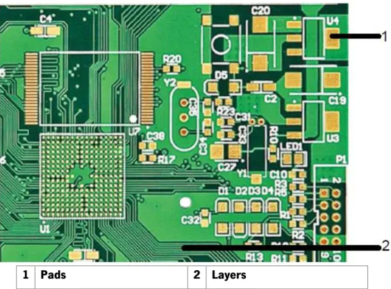
1 Pads
2 Layers
Figure 1- PCB example [3]
Figure 2- PCB with 2 Layers
The base material, the substrate, firstly made of phenolite, mixture of phenolic resin with
a quantity of shredded paper, is now made of fiberglass. With the phenolite mixture the PCB
8
absorbs more humidity and can be more easily damaged. [4]. For this reason the fiberglass was a
great choice to substitute this mixture. This boards are made of epoxy resin with a thin sheet of
fiberglass and gives the necessary rigidity and thickness to the PCB, Figure 3. There are some
thicknesses that can be used in PCBs but the most usual is 1.6 mm. This layer is also useful to
protect the conductive tracks of touching each other.
Figure 3 - Fiberglass-resin laminate (FR4) [5]
On the top of the substrate a thin layer of copper can be found. The thickness of this layer
depends on the purpose of the PCB.
The soldermask, Figure 5, gives to the PCB the green colour and insulate the copper from
accidental contact with other metals. This layer is applied to the majority of the PCBs and leaves
the pads
1exposed so the components can be soldered later, Figure 4. In Bosch Car Multimedia
the soldermask used are Organic Solderability Preservatives (OSP), tin (Sn) and Nickel - Gold
(NiAu).
9 Figure 4 – Pads [6]
The last layer is applied after the soldermask and it can add text, numbers or symbols to
the PCB in order to facilitate the assembly, Figure 5. This layer is optional.
Figure 5 - PCB with soldermask and silkscreen [7]
2.3 PCB Assembly Line Evolution
The PCB line production has been developed through the years and the support of today’s
lean production systems is dated from the beginning of the industrial revolution in the 18
thcentury.
As it can be seen in Figure 6, Randsom Olds [8] created the first modern patented assembly line
in 1901, increasing the output of his factory of 500 percent in on year using this process. His
factory was able to produce 20 cars per day and his car was simply to assembly and cheaper.
Later, Henry Ford, Sakichi Toyoda or William Edwards Deming developed this process but it was
Taiichi Ohno and Shigeo Shingo who developed the Toyota Production System, TPS [9], which gave
10
the biggest step studying the American production system and applying that to the Japanese reality
of the time. Later, Ohno and Shingo have applied new approaches to the industrial production.
This new approache can be resumed in:
The inputs /outputs process is modelled and treated as a flow of materials and
information;
The process analysis is made with the help of two axis – materials flow and
operator flow;
Reformulation of the loss concept that includes the transportation, stock,
inspection and rework of the product.
According to James P. Womack [10], the lean production is used to combat the production
waste. The objective of the
just-in-time (JIT) production is the continuous improvement of the
production process. The stock reduction, waste elimination, the continuous flow and the
improvement of the processes are some of the JIT characteristics.
Companies like Porsche, BMW, Ford or even Bosch have been working in their own
production systems. The ambition to produce quickly or efficiently in order to respond of the
customers’ needs in a competitive environment is common to all of these companies.
11
2.4 Bosch Production System (BPS)
The Bosch Production System (BPS) was introduced in 2002. This system was
implemented after a costumer critical feedback in 1999 and was the first subsystem of the Bosch
Business System (BBS) that can be seen in Figure 7.
Figure 7 - Bosch Business System (BBS)
With the analysis of different production lines and factories, Bosch has improved its
guidelines for production planning, manufacturing, re-design the production systems, etc. The
BOSCH target is to reduce the waste and guarantee the long term profit and growth of the company.
The production waste can be caused by many causes like:
Overproduction – production above than the customer ordered;
Excessive stocks – can cover the really production problems;
Space – two large areas cause long routes and increase the production time;
Unnecessary movements – non-ergonomic tools or workpieces can take to
more than the necessary movements;
Transport – can occur transport damage or increase the costs;
Waiting times – periods with non-activity and can take to reduced productivity;
Errors/rework – can increase the manufacturing costs and damaging the
company image.
12
The Bosch Production System is based in eight principles that can be seen in Table 1.
Table 1- Bosch Production System Principles
Pull Principle
Produce and supply only what the customer wants
Fault Prevention
Avoid errors
Process orientation
Develop and optimize the processes
Flexibility
Adapt the products and services to the customer requirements
Standardization
Standardize processes and implement the best solutions
Transparency
Deviations from the target are immediately apparent
Continuous improvement
Continuous developing
Personal responsibility
Competencies and responsibilities are well known
There are many methods that can be used to improve the production. An example is the
5S method that is used to improve order and cleanliness at the workplace. This method is
supported by five characteristics:
Sort / Seiri – remove unnecessary things from the workplace;
Straighten / Seiton – ergonomic arrangement of all objects;
Sweep / Seizo – clean the workplace;
Standardize / Seiketsu – set standards;
Self-discipline/ Shitsuke – maintain standards.
To have a good production process is important that exists an oriented flow layout. This
oriented layout is used to decrease the waste material and to optimize the line flow. Thus the flow
is oriented so that the production line is continuous, optimized and avoids chaos and confusion.
13
CHAPTER 3 PCB
A
SSEMBLY
L
INE
In this chapter is made an introduction to the entire line of the PCB assembly. Starting in
the handling of the PCB, and passing through the solder paste printing or reflow and ending in
Manual insertion it will be presented all the entire line and the important parameters of all the
processes used at Bosch Car Multimedia.
As we can see in the following lines of this document, the production line, its evolution and
the way the processes are made is an important key to the PCB assembly and the reduction of the
production scrap and defects. All the processes are important to the final quality of the PCBA but
also the cleanliness of the line or the way the employees are trained are also important.
3.1 PCBA in the BOSCH CM
In the Bosch CM, PCBA line is divided in two distinct lines. One for the first side of the PCB
(Figure 8) and the other one to mount the radial components and the second side of the PCB
(Figure 9).
Figure 8 - PCBA line (side A) Table 2 - Figure 5 caption
A Loader D Solder Paste Printing G Reflow
B Laser Marking E SPI H Fifo / Buffer
14
Figure 9 - PCBA line (radial insertion and side B)
Table 3 - Figure 6 Caption
J
Loader
N
Adhesive dispensing
K
Radial Insertion
O
SMD Placement
L
Inversor
P
Reflow
M Shaker
Q
AOI
With the improvement of the Surface Mount Technology the manufacturers are increasing
the production speed and decreasing the scrap costs. Is important that the PCBA line is fast enough
to follow the production requirements and while scrap is reduced. In all processes the employees’
training is important as well as the existence of work instructions explaining the correct procedures
in each machine and production line.
3.2 General Requirements for the production line
There are some parameters that the production line has to fulfil to guarantee the quality
parameters. In general the line has to be perfectly clean and follow some standard specifications
related to temperature or humidity. Thus, the temperature has to be between 18ºc and 30ºC and
the humidity between 40% and 60%.
15
Cleanliness: the cleanliness must be kept in levels to prevent the contamination
of the surfaces to be soldered. Eating or smoking in the production area is forbidden to prevent the
contamination of the PCBA.
Electrostatic Discharge: All the working areas, to prevent and control
electrostatic discharges, must have test stations like a turnstile and must be marked has ESD
protected areas (EPA), in Figure 10 can be found an example for the ESD logotype.
Figure 10 - Examples of ESD logo
The operator must use cloths and shoes to prevent this electrical discharges and for that
they must use ESD shoes, or foot conductive shoes, ESD safety coat fully closed, ESD protective
gloves and, if necessary, a cap.
Moisture Sensitive Device: the storage and handling during PCB assemblies
are clearly defined in IPC/JEDEC J-STD-033C – “Handling, Packing, Shipping and Use of
Moisture/Reflow Sensitive Surface Mount Devices”, J-STD-020D and IPC-1601 – “Printed Board
Handling and Storage Guidelines”.
A single mistake with moisture sensitive devices can cause a “negative impact on the entire
production batch” [11]. The moisture sensitive devices are packaged in a moisture barrier antistatic
bag, Figure 11, with a moisture indicator card and a desiccant, Figure 12.
16
Figure 11 - MSD Dry Bag [12]
Figure 12 - Humidity indicator and Desiccant [12]
The Humidity Indicator Card (HIC) indicates how much moisture the dry pack contains,
the circles turns into pink when there is some humidity in the bag. The desiccant prevents
damages, like corrosion, caused by humidity.
In the production area must exist a dry cabinet and also a baking oven. The dry cabinet is
used to temporary stock the MSDs removed from the dry pack and that are waiting for the soldering
process while the baking oven is used to bake MSDs and restore their floor life to the initial value
[11].
17
3.3 PCB Handling
The handling of the PCBs, electronic components and also PCBA are really important for
the final result. The handling requires precaution and care. A careless handling can take to
electrical shocks or fails and may lead to an accumulation of static charge on the board and destroy
the components. To avoid these, are some safety requirements that can be followed:
The use of gloves and safety cloths are some of the safety requirements but also
the work areas must be clean and free of static materials;
During the production no contamination due to fingerprints may reach the active
surface of the PCB and it should be touched only on the PCB frame.
To prevent some handling damages must be avoided:
Hand cream and lotions containing silicone;
Stacking of PCB’s assemblies and PCB.
Some requirements due to the storage of the PCBs have to be taken in consideration:
Is not allowed more than 100 PCBs in the same package and more than 200 in
the same pile;
ESD packaging must be used;
All PCBs must be in the same horizontal position;
The transport of the PCBs must be adequate;
The PCB handling is not permitted after the reflow soldering.
Some of these requirements like, PCB transportation and handling, help prevent the PCB
warpage. The maximum warpage for PCBs with 1.6mm of thickness is 0.7%, as can be seen in
Figure 13.
18
3.4 PCB Laser Marking
To improve the production and to make the production faster it was implemented a process
that may help the identification of the product. This process will make the assembly faster and
guarantee that there is no errors or exchanges in the production line.
The laser marking makes high quality and safe marks in many types of materials. This
process is applicable to all PCB’s and each PCB has to be marked with an individual code in the
appropriate area. With the implementation of this process, the electronic industry attain better
results and better products and helps also the improvement of the quality and the effectiveness.
This technology is widely used in electronic products and, in this case, the 1D barcode, 2D data
matrix code and some human readable text are marked in each PCB [13]
.The laser marking does not contact directly with the PCB and, for that, there is no
mechanical extrusion, tension, the physical proprieties are not changed and the affected region is
lesser than with other processes.
This process is controlled by a computer, which makes possible the storage of various
codes, layouts and positions. The 1D barcode, Figure 14, is used to the identification of the PCB’s
during the insertion and in the final assembly lines while the 2D data matrix code, Figure 15, is
used for traceability. The human readable text, Figure 16, are optional and exist to distinguish two
different products that shares the same PCB.
19 Figure 15 - 2D Data Matrix Code [14]
Figure 16 - Human readable text [14]
All these codes have to follow rules and have a specific size defined by Bosch Car
Multimedia.
Is important, to the correct function of the machine that the maintenance plan exists in the
production. The laser filters and the gas tube should be changed when the lifetime is reached.
3.5 PCB Cleaning
Is important that the PCB is perfectly cleaned and the contamination sources must be
eliminated from the PCBs. A small particle of dust can spoil the PCBA production. Therefore, a
bare board cleaner with an ionized air blow and vacuum must exist after the laser marking and
after any build-up charge, unpacking, and before printing.
In the cleaning machine, to prevent from the cumulated dirtiness in the ionized bars, must
exist an electrostatic sensor. This control should be 100% done and automatic and the control must
be done once per month directly at the ionized bar.
3.6 Solder Paste Printing
The solder paste printing process is one of the most important process of all line. A bad
paste printing can influence more than one process. To prevent some error that can pass in the
solder paste printing we also have the Solder paste printing inspection but, as we can see further,
is not a perfect process too.
The joints between the cooper and the tracks are, normally, soldered with the help of solder
paste. This process consists in the automatic deposit of solder paste on the top of the PCB in
places that an electrical connection to component terminals is required. This deposit is applied in
20
a pattern using a stencil that only allows to leave solder paste where is necessary. With this process
is easier to achieve difficult places and prevent the surface oxidation.
The solder paste is a homogeneous mixture between solder metallic particles of solder
alloy, with solder flux. This flux ensure that the metal surfaces are free of oxides at the time the
metal joint is formed [15] and the solder paste is used to facilitate solder, directing the solder to
the right place [16]. This process comprises a stencil, a squeegee and an automatic stencil wiper
to clean the stencil.
Is important that the printing parameters are well defined to have a good quality on the
solder printing and to have this quality the printing depends on the:
Squeegee speed;
Squeegee pressure;
Separation speed;
Squeegee angle;
Printing mode;
Separation way;
This characteristics are important to the quality of the solder paste printing.
Solder Paste
There are many types of solder pastes. They can be lead with tin, antimony, silver or can
be lead free and be a moisture of tin, silver and copper.
With the increase of the health and environmental concerns, the usage of lead solder paste
was limited. Although, this limitation, has stimulated the development and use of the lead-free
alloys in the electronic industry. According [17], in 1995 the world Pb consumption was about five
million tons. At this time the industrial purpose is to find a nontoxic and low melting temperature
alloys to replace this Pb value.
The lead free, compared to lead solders, are more expensive, the melting point is higher
and the lead free pastes may increase the uplifting of smaller components because of the reduced
wetting behaviour. For all this examples the lead free must carefully be choose and may not
21
decompose or vaporize at the melting point of the alloy [18]. The lead free alloys must ensure a
productivity and reliability at least equivalent to the levels of Sn-Pb solders.
This type of solder pastes reflects the light differently and because of that the procedures
to verify the quality of the solder meniscus is different than compared to lead solder pastes. [19]
The solder paste has some components that can be injurious to the human been. For this
reason the operator must follow some rules:
Must use gloves;
Must use protector glasses;
Pregnant woman are forbidden to work with solder pastes.
3.7 SPI – Solder Paste Inspection
After the solder paste printing process the PCB passes through the SPI machine. In this
process the solder paste printing are analysed and the main task of the SPI is to find pads which
are not well printed. The SPI process can help the improvement of Solder Paste Printing process
minimizing the rework and reducing the scrap and the costs. It can also be used for traceability.
This process are not precisely in small and micro solder paste deposits and can fail if the printing
defects are localized in these deposits.
The paste printing process must be stable and there must be uniformity of the printing
deposits shape. There are many reasons for the pads variation like the:
PCB warpage;
Solder resist thickness;
Accuracy of fiducial mark recognition;
Stencil deformation;
Squeegee condition;
Stencil cleaning performance;
22
The SPI limits should be previously defined and some kind of errors can be classified as
“pass” if they were not a risk to the process.
3.8 SMT – Placement
This method of mounted directly the component in the surface of the PCB was developed
in 1960s and nowadays all electronic hardware is manufactured using this technic. This process
doesn’t use holes in the PCB and it allows that the components evolved through the years and now
are smaller and with an increased functionality.
This process allows the use of smaller components and smaller PCBs, although the
manual assembly and the repair is more difficult in this process It also allows higher component
density in the PCBs. With this advantages and adding:
Lower initial and production costs;
Faster production;
Components can be placed on both sides of the PCB.
this process is more stable and better performing in shake and vibration conditions than
the Through Hole Technology. [20]
Figure 17 - Common Surface Mount Devices [21]
3.9 Automatic Optical Inspection (AOI)
Nowadays, with the downscaling of the components size, the increase of the PCB density
and the high productivity of the PCBA lines is expected a high quality in the end of the production.
So, after the assembly sequence, more precisely after the reflow, the PCBA is inspected in AOI
machine.
23
This non-contact and non-destructive process determine, with the help of the geometric
and optical properties of the solder meniscus, the quality of the solder joints [19]. The sooner a
failure is detected the sooner the production is improved. The AOI have also disadvantages, this
process can’t inspect hidden failures and it’s not fast enough to follow the line production.
The solder paste type can influence the AOI results. To avoid errors the setting may have
to be adjust according lead-free or lead solder pastes.
3.10 Through-hole Technology
The Through-hole technology is the technology that inserts components in holes drilled in
the PCB and, after, clinch the leads of the component on the PCB. This technology is used for
years and is increasingly less used in these days. The radial and axial components are less used.
This technology can be divided in Radial and Axial insertion. The radial components can
have two or three leads and are inserted perpendicular to the PCB (Figure 18). Although, the axial
components have two axial leads in the axial axis of symmetry, like the Figure 19.
24
Figure 19 - Axial components insertion [22]
The radial insertion consists in the insertion of the radial components and clinching them
in the PCB. The Figure 20 shows an example of the radial insertion.
Figure 20 - Radial Insertion
Through-hole is ideal for components that might be under mechanical stress. But, on the
other hand, this process requires drilling holes, and the use of wave, selective or hand soldering
which are not trusty and repeatable. For all of these reasons this process is too expensive.
With the evolution of the Surface Mount Technology the THT is not so used has it been
before.
3.11 Adhesive Dispensing and Curing
The electronic components are more and tinier and to not lose the component in when the
board is rotated for the soldering of the A Side components, the B Side components are glued to
25
the board with the help of the adhesive dispensing and curing process. This process consists in
the transfer of the precise size of adhesive onto the PCB holding the SMD components until wave
or reflow soldering process.
There are lots of factors to consider when talking of adhesive dispensing, the equipment,
method, materials, environment and operators are fundamental to have a good dispensing but the
most important factor to this process is the dispensing head and also the type of adhesive that is
used.
The adhesive dot is defined by the viscosity, pressure, dispensing time, auger rotation,
piston strokes number, dispense rate and nozzle standoff height [23].
There are three dispensing systems available:
Time and Pressure system (Figure 21) – the adhesive is dispensing with the help
of high pressure applied in the top of the adhesive cartridge.
Figure 21 - Pressure System (Adapted) [23]
Auger Pump system (Figure 22) – is applied a constant low pressure in the top of
the cartridge until the adhesive reaches the top of the chamber, then when the auger is rotated the
adhesive is dispensed.
26
Figure 22 - Auger Pump System (Adapted) [23]
Piston Pump system (Figure 23) – This kind of system is the most precisely and
have a variation of ± 1% by volume. When the piston reaches the valve, a constant and low pressure
is applied in the top of the cartridge.
27
3.12 Soldering
The soldering process is used to attach electronic components to a printed circuit board and
to made the transition of the component to the board. There are three automated methods to do
this, wave soldering, selective soldering and reflow.
While reflow takes the PCB to a certain temperature above the melting point to allow the
welding of the components, wave and selective soldering exposes the PCB to a molten wave of
solder. Selective and Wave soldered are two distinct processes. In the wave soldering the entire
PCB passes through the wave while, in selective soldering, only certain connections are soldered
[24]. There are many types of solder that can be used.
3.12.1 Reflow
The electronic industry uses the reflow process for many years but, with the development
of the SMT process, the Reflow soldering has been studied and explorer as never been before.
After the printing and the placement of the SMD components the PCB is placed into the oven. At
this time the PCB is raised to a temperature above the melting point of the solder alloy to allow the
welding of the components and get the optimum solder joint quality. The nitrogen atmosphere may
reduce the oxidation and may help to the solder joint quality too. The solder used by Bosch Car
Multimedia is SAC405.
The goal of the reflow soldering is to have a uniform and clean solder joint in a minimum
time without overheating and damaging the components.
To insure a good reflow should be considered [26]:
PCB thickness
Solder mask applied on the PCB
Quality of the solder paste
The design of the stencil
The equipment used for the reflow
28
Below are a common reflow soldering profile, Figure 24.
One of the most important factors in the reflow process is the temperature profile [25].
The profile is divided in several stages and must be adapted to all the components types, different
components and the components with different thermal mass may not reach the ideal temperature
at the same time. In Figure 24 is represented a general reflow profile.
Figure 24 – General Solder Convection Reflow Solder Profile [25]
There are four stages in a conventional reflow soldering:
Preheat zone: Is the longest zone in all reflow and is when the heating ramp is
defined. This heating allows the remove of impurities, reduces the thermal shock and prevents
damages in the components.
Thermal Soak: The second zone have the function of activate the flux to remove
the oxides from the PCB and to balance the temperature on the board. The temperature used in
this zone is very important, a high temperature can take in extreme to the oxidation of the paste
whilst if the temperature is too low the soldering cannot start. This stage is important to reduce
voiding.
Reflow: The maximum temperature is reached on the reflow zone and the limit
for this temperature is achieved by the component with the lowest tolerance for high temperatures.
29
Some cares should be followed to not exceed the temperature limit and damage some components
and to have a perfect formation of the solder joint. At this zone, the time is really important and
should be monitored. In this phase the maximum temperature is achieved.
Cooling: The last zone, cooling, is used for the solidification of the solder joints.
This zone prevents the formation of intermetallic excess or the thermal shocks to the components.
Is usually used a temperature of 4ºC. The solder paste will solder wise if the time to achieve reflow
is shorter. [27]
3.12.2 Wave Soldering
This process is used for through hole or surface mount assemblies to solder the leads of the
components to the board. In this process the bottom of the PCB is literally washed with a molten
solder. Wave soldering is faster than selective soldering because the PCB is soldered all at the
same time but is just ideal for boards with conventional leaded components and some larger
surface mount components. The solder used by Bosch Car Multimedia is SAC305. In Figure 25 is
represented a scheme of wave soldering process.
The process have three zones:
Fluxing Zone (A) – in this zone is applied a flux spray to ensure that the areas
to be soldered are clean free from oxidation. Two little flux can take to poor joint while too much
flux may take to residual flux on the board.
Preheating Zone (B) – this zone uses convection or infrared heaters to increase
the PCB temperature and remove humidity. The flux is activated and the thermal shocks are
prevented.
Soldering Zone (C) – a melted solder wave is pumped to the PCB. The board is
soldered all at the same time and with two different waves. The first wave has the objective to reach
all the board while the second wave is bigger than the first and removes the excess of solder.
30
Figure 25- Wave Soldering Scheme (Adapted) [28]
3.12.3 Selective Soldering
Not all components can be exposure to high temperatures and cannot be damaged by the
heat of the reflow oven or wave soldering. For PCBs that have this type of components the selective
soldering is one option. This soldering process is sufficiently precise and can solder the necessary
components without touching the sensitive components.
This programmable machines uses a small solder wave that only passes through the
components that need to be soldered. In this process, as used in wave soldering, applies a flux in
the areas to be welded, avoiding any sensitive components. In the next step the solder pot rises to
solder the through hole leads to the PCB.
Selective soldering is slower than wave soldering but this process can be customized to any
PCB configuration or any heat sensitive components.
31
3.13 X-Ray
With the increase usage of BGAs (Ball Grid Arrays), Figure 26, where the connections are
under the component and not visible, it was necessary to improve the inspection technique and
guarantee that the hidden features are examined. So, the only efficient method to control this types
of components is the Automatic X-Ray inspection. This process is available in 2D or 3D and it
detects soldering defects.
Figure 26 - X-Ray inspection of BGA [29]
This process used for the evaluation of the solder joint and component allows the
identification of possible soldering failures like:
Shorts;
Opens;
Insufficient / excessive solder;
Missing electrical parts;
Misaligned components:
Voiding.
32
Regarding inspection, are also many differences between a lead free and a leaded based
solder joints. While a lead based solder joints (SnPb) have a bright surface, the lead free doesn’t
have this bright surface. It presents a grainy solder joint caused by the irregular solidification of the
solder. Thus the solder paste inspection have to be adjusted every time is inspected a led based
or a lead free solder joint.
X-Ray images are acquired by positioning the PCB sample between a focused beam of
x-rays and a proper detector, Figure 27. The sample is irradiated by an X-Ray source and is projected
into the x-ray detector.
Figure 27 - Static X-Ray Scheme [31]
Measurement data from X-Ray inspection permits to the operator to implement real-time
process control giving information to improve the quality of PCBA [30]
33
CHAPTER 4 P
RESENTATION AND DISCUSSION OF THE RESULTS
To be able to answer to the customer requirements and with the increase of the production
volume, it may be necessary to find others factories to produce for Bosch. Although, it is necessary
that these products fulfil the customer and Bosch CM quality criteria. With this need it is necessary
to standardize all production lines and to pass some quality criteria for the new supplier. For this
reason it became necessary to develop a document that can be consulted by the new supplier and
helps him to fulfil the Bosch CM requirements.
In this chapter is made the description of the entire work that can be found in Appendix I
and a checklist is presented that can be used in external workbenches evaluation in Appendix II.
For this work it was necessary the study of the entire line procedures and parameters that
can influence the PCBA production. It was made a data collection from all Bosch requirements
documents and was adapted to a checklist sheet to help the approval of new lines.
In section 4.1 is described the method used to produce the document that supports the
implementation of the PCBA line. It Is shown, in detail, the issues that the factory has to deal to
make a PCB with the Bosch quality requirements and, in section 4.2, is described the Technical
Assessment Checklist that was made in order to facilitate the implementation of a new line outside
the Bosch CM factory.
As can be noticed throughout the whole document there are some important factors that
influence the quality of the PCB assembly. All the machines and processes have their influence in
the final result and the handling of components and PCB’s are also important. A careless handling
can cause electrical damages. For this, the use of gloves, boots or coats are indispensable to the
production. But also some processes have more influence than others and the quality of the solder
34
paste printing and the respective machine are one of the most important processes in these
assembly lines.
For these reasons, in section 4.3 is made a full description of the solder paste printing
process. Is also made the description of the conditions that the new supplier as to follow to have a
good printing and have a final product with the quality of an in house product was. The entire line
processes and the descriptions for all the other processes can be found in appendix I and II.
4.1 Outsourced Process and Extended Workbenches of Electronic
Assemblies
For this project it was elaborated an document to help the implementation of the Bosch
quality criteria in the new PCBA supplier (appendix I). This document was made to facilitate the
approval of a new line production in a new factory outside Bosch Car Multimedia. This production
flow has to respond to Bosch CM requirements and quality levels.
To obtain a good implementation of new assembly lines in the new factory, the structure
of document is very important. For this reason, the document was divided in ten chapters and in
chapter 6 can be found the mandatory requirements for the flow line.
Starting with the general considerations that have to be taken in account this document
goes through the flow line, from the laser marking to the manual reflow of the boards. So, the
processes described are:
PCB Handling;
PCB Marking;
PCB Cleaning;
Solder Paste Printing;
Solder Paste Printing Inspection;
SMD Placement;
Reflow;
35
Radial Insertion;
Adhesive Dispensing and Curing;
Wave Soldering;
Selective Soldering;
X-Ray Inspection;
Pin Insertion;
Conformal Coating;
Gap Filler;
Manual Insertion;
Mechanical Clinching;
Repair / Rework;
In each process the most important values and parameters that have to be used to have
a good PCB assembly with Bosch CM quality were discussed. Thus, all chapters follow the same
structure. Beginning with the general parameters of the process when applicable to the process,
the document specifies the:
Environment;
Storage;
Handling;
Materials;
Tools;
Cleaning;
Maintenance;
Process Control;
Machine Capability (CmK);
36
Process Capability (CpK).
All the processes are important for the PCBA quality but, with the research and
development of this thesis, it was easy to notice that some parameters and some type of processes
are more important to the final result than others.
4.2 Technical Assessment Checklist
The Technical Assessment Checklist was based in the Outsourced Process and Extended
Workbenches of Electronic Assemblies requirements (appendix II) and was created to help the
implementation and to guarantee that the quality requirements were fulfilled (see example in Figure
28).
Figure 28 – Technical Assessment Checklist example sheet [appendix III]
This checklist has to be simple, objective and with easy visualization. For this reason the
checklist document, as well the requirements, was divided in all processes. It contains the general
requirements and then the flow line is documented with the right order of PCB assembly. In Figure
29 can be found the solder paste-printing example of the checklist document. The checklist shows
the topics that the factory has to fulfill and the exact chapter that can be found in the requirements
document to facilitate the implementation (Appendix III).
37 Figure 29 – Technical Assessment Checklist example of Solder Paste Printing Process
To assure that all these topics were implemented, all the sheets were divided in three
stages. The first one is executed by supplier, and the other two by Bosch, in the supplier site, one
in test mode and the other in production mode (Figure 30).
Figure 30 – Stages of the evaluation
A rating table helps to validate the flow line, Figure 31. This rating grade has 5 levels:
No – 0%;
Partially – 25%;
Essentially – 50%;
Nearly Complete – 75%;
38
Figure 31 - Ratting Grade
In Figure 31 is noticeable that every time the parameter is not completely fulfilled is
generated an OPL – One Point Lesson. This OPL has the objective to help the supplier to correct
the points that are in fault and fulfil all the Bosch parameters and the required quality.
In the end of every sheet exists a “not allowed” section that remembers the things, to
supplier, that shall not happen in the progress of the flow.
4.3 Solder Paste Printing
All processes contribute to product quality. In this thesis the Solder Paste Printing process
is studied in detail. This process can influence the entire flow line and bring, in the end, defects
that the factory does not want to reach the client.
Studies made shown that approximately 50% of all electronics assembly (Figure 32) errors
and 65% of SMT defects (Figure 33) are associated to solder paste printing and solder joint
formation [33].
39 Figure 32 - Defect Chart for All Electronics Assemblies
Figure 33 - Defect Chart for SMT (only) Assemblies
It can be concluded that the majority of product defects are originated in the solder paste
printing and are detected only in Solder Paste Inspection. For this, the improvement of this process
is a big challenge for all the factories.
0% 2% 4% 6% 8% 10% 12% 14% 16% 18% 20% 0% 5% 10% 15% 20% 25% 30%
40
In this work the solder paste printing process will deserve special attention and in this
chapter will be explained all the conditions that the supplier has to fulfill to comply with Bosch
qualities demands.
To begin, the production line and processes have to fulfill some generals requirements.
The solder paste printing machine has to be fully automatic and must have a computer controlled
printer with an automatic stencil and wiper to clean the solder paste residues. The stencil must be
fixed with a clamping system and the PCB must be centered with the use of fiducials and an
automatic optical system.
The fiducial are recognition marks and are used to locate the position of all features on as
individual PCB. They can be [34]:
Panel Fiducials – are located in the fabrication panel outside the perimeter of
the PCBs;
Global Fiducials – located on the PCB, usually in the four corners of it.
Local Fiducials – used to locate the position of an individual component;
The fiducials marks can have various shapes as can be seen in Figure 34. A bad alignment
can take to a bad printing or a bad insertion of the components affecting the final PCBA.
Figure 34 - Common used Fiducials [34]
The warpage of the PCB has to be avoided and the squeegee pressure deserves special
attention not to pass the maximum admissible warpage. In Figure 13, can be found a scheme of
the maximum admissible warpage for a PCB with 1.6mm of thickness. To reduce the warpage
issue may be provided a support for the PCB.
41
4.3.1 Environment
The local environment has to be controlled and must be according the Bosch CM
requirements. The humidity and temperature has to be between the values referred on Table 4.
Table 4 - Minimum and Maximum Allowable Temperature and Humidity
Minimum Admissible
Maximum Admissible
Temperature
18ºC
30ºC
Humidity
40%
60%
As can be seen in section 3.6 the solder paste quality influences the final quality of the
solder. In Bosch Car Multimedia the solder paste in use is Heraeus F620 Cu0.5-88M3 and the
specifications for this solder paste can be found in Table 5 and in appendix III. A good printing can
help the increase of the long-term reliability of solder joints. To have a good printing and later a
good solderability, the solder paste has to be maintained at a determined temperature and humidity
defined by the supplier.
Table 5 - Heraeus F620 Specifications
Solder Alloy
Sn 95.5/Ag 4/Cu0.5 in accordance with DIN EN 29453
Metal Content Standard 88% ± 0.5%
Melting Point
217ºC
4.3.2 Storage
The storage of the solder paste is important for the right printing and consequently for the
quality of the PCBA. For that the solder paste has to be storage according the supplier specifications
and must be scraped if the specifications are not fulfilled. The usage timeline can be found in
Figure 35.
42
Figure 35 - Usage Timeline for Solder Paste


![Figure 17 - Common Surface Mount Devices [21]](https://thumb-eu.123doks.com/thumbv2/123dok_br/17613028.820412/41.892.108.741.720.900/figure-common-surface-mount-devices.webp)
![Figure 24 – General Solder Convection Reflow Solder Profile [25]](https://thumb-eu.123doks.com/thumbv2/123dok_br/17613028.820412/47.892.126.723.311.619/figure-general-solder-convection-reflow-solder-profile.webp)
![Figure 25- Wave Soldering Scheme (Adapted) [28]](https://thumb-eu.123doks.com/thumbv2/123dok_br/17613028.820412/49.892.111.747.117.532/figure-wave-soldering-scheme-adapted.webp)
![Figure 26 - X-Ray inspection of BGA [29]](https://thumb-eu.123doks.com/thumbv2/123dok_br/17613028.820412/50.892.292.641.353.662/figure-x-ray-inspection-bga.webp)
![Figure 27 - Static X-Ray Scheme [31]](https://thumb-eu.123doks.com/thumbv2/123dok_br/17613028.820412/51.892.264.582.421.818/figure-static-x-ray-scheme.webp)
