Tomás Colaço Ribeiro Fernandes
Bachelor Degree in Micro and Nanotechnologies Engineering
Digital Fabrication of Transparent Electrodes for
Simultaneously Optical and Electrochemical
Biosensor Applications
Dissertation submitted in partial fulfillment of the requirements for the degree of Master of Science in Micro and Nanotechnologies Engineering
Adviser: Dr. Elvira Fortunato, Full Professor, Faculty of Science and Technol-ogy, NOVA University of Lisbon
Co-adviser: Dr. Maria Goreti Sales, Adjunct Professor, School of Engineering of the Polytechnique School of Porto
Digital Fabrication of Transparent Electrodes for Biosensor Applications Using Spectroelectrochemical Analysis
Copyright © Tomás Colaço Ribeiro Fernandes, Faculdade de Ciências e Tecnologia, Universidade Nova de Lisboa.
Electrochemical Biosensor Applications
Acknowledgements
A realização desta dissertação marca o final de uma importante e árdua etapa da minha vida. Como tal, gostaria de agradecer a todos aqueles que contribuíram para a sua concretização. Muitos nomes ficarão por mencionar, porém o vosso apoio tem e terá sempre um apreço incondicional da minha parte e deixo-vos o meu mais sincero agradecimento.
Primeiramente, quero agradecer à minha instituição, a grande Faculdade de Ciências e Tecnologias da Universidade NOVA de Lisboa e ao departamento de Ciências dos Materiais por todas as aventuras e grande espírito académico ao longo destes cinco anos.
À minha orientadora, Professora Elvira Fortunato, pelo seu conhecimento, disponibilidade e excelentes condições de trabalho que proporcionou não só nesta fase, como também ao longo de todo o curso. Estendo este agradecimento ao Professor Rodrigo Martins, pela sua visão e dedicação na criação do curso de Engenharia de Micro e Nanotecnologias.
À minha coorientadora, Professora Goreti Sales, pelos seus conselhos, confiança e ajuda pela criação de financiamento.
À Dr. Manuela Frasco pela paciência, brainstorm e acompanhamento e a todo o
grupo do BioMark pelos braços abertos com que me receberam, pela boa-disposição contagiante e suporte moral. Destaco também a Sara, a Rita e a Carla por tudo o que me ensinaram.
A toda a equipa do CENIMAT pelo trabalho excecional que fazem. À Ana Samouco pelo acompanhamento inicial, amizade e resposta a todas as perguntas estapafúrdias. À Sofia Ferreira por toda a ajuda, orientação, horas de deposições e explicações. À Carolina Marques pelo seu apoio incessante, pelas inúmeras ideias e atenção. À Professora Rita Branquinho, por ter sido a melhor professora que tive, por ser sempre prestável e me ter aberto esta porta.
À minha família e amigos, pelo suporte, compreensão, motivação e amor. Aos amigos do cinema pelas conversas idiotas, aos amigos dos jogos tardios pelos momentos de relaxamento e aos amigos da praxe, por todos os escapes que me ofereceram. Ao Dimi, ao Gui, ao Miguel, ao Moura e aos meus afilhados.
À minha mãe, por ter dado tudo o que tinha para que o meu futuro fosse melhor e por fazê-lo sozinha, incansavelmente. Ao meu avô, que sempre se sacrificou por mim e foi o pai que nunca tive.
Electrochemical Biosensor Applications
Resumo
Esta dissertação propõe um biossensor pioneiro para deteção de biomarcadores de cancro, que combina um reconhecimento eletroquímico e ótico na mesma análise, ao tirar partido da padronização de elétrodos transparentes e flexíveis a partir de escrita direta por laser. O biomarcador, o antigénio carcino-embrionário, é detetado por um material biomimético semelhante a um anticorpo. O sensor produzido sobre vidros de óxido de índio dopado com estanho (ITO) consiste num cristal fotónico composto por nanopartículas de sílica incorporado num filme de polipirrole molecularmente impresso, obtido através de eletropolimerização de pirrole na presença do biomarcador. A interação entre o biomarcador e o material sensor traduz-se em sinais eletroquímicos capazes de gerar dados quantitativos. Simultaneamente, desencadeia uma diferença na reflectância da matriz do filme sensor, permitindo também o estudo do sinal ótico. Assim, as características analíticas do biossensor foram estudadas por Espetroscopia de Impedância Eletroquímica e pela refletância da estrutura opala do cristal fotónico, tendo apresentado resposta a concentrações fisiologicamente relevantes (entre 2.5 ng/mL e 10 ng/mL). Este sensor foi construído num substrato de ITO como prova de conceito, sendo este o melhor óxido entre vários materiais condutores produzidos em substrato de vidro, mesmo que a primeira parte do trabalho se concentre na preparação de filmes finos de óxido de
zinco dopado com alumínio através de sputtering de radiofrequências e no fabrico de
elétrodos através de escrita direta por laser. Estes processos foram otimizados para a fabricação de óxidos altamente condutores e transparentes, capazes de, no futuro, substituir o ITO como componente principal na indústria de eletrónica transparente e flexível.
O dispositivo sensor desenvolvido demonstrou potenciais características em termos de alta sensibilidade, estabilidade e dupla deteção, que o podem vir a tornar uma solução portátil, mais simples e de baixo custo para a deteção de CEA no local de prestação de cuidados quando comparado a métodos imunológicos convencionais. Simultaneamente, poderá abrir novas portas para outras aplicações e melhorar as perspetivas em termos de diagnóstico precoce de doenças.
Electrochemical Biosensor Applications
Abstract
This dissertation proposes a pioneering biosensor for detecting cancer biomarkers that combines electrochemical and optical recognition in the same analyzing spot, by taking advantage of laser direct writing to pattern transparent and flexible electrodes. The bi-omarker, the carcinoembryonic antigen (CEA), is detected by an antibody-like biomi-metic material as recognizing agent. The sensing film over indium tin oxide (ITO) coated glass substrate consisted of a molecularly imprinted layer of polypyrrole (PPy). The im-printed film is assembled on a three-dimensional photonic crystal composed of silica na-noparticles (NPs), allowing optical detection. The molecularly imprinted polymer was obtained through electropolymerization of pyrrole in the presence of the biomarker as template. The interaction between the biomarker and the sensing material produces elec-trochemical signals generating quantitative data. In addition, it triggers a difference in the reflectance of the sensing photonic film matrix. The analytical features of the biosensor were assessed in PBS buffer by electrochemical impedance spectroscopy (EIS) and by reflectance of the opal-based photonic crystal. The response of the proposed biosensor was in the range of physiological relevant levels of CEA (from 2.5 ng/mL to 10 ng/mL). This sensor was assembled on an ITO substrate as proof of concept, the best substrate among the several conductive material produced on glass support, even if the first part of the work focuses on the preparation of aluminum doped zinc oxide (AZO) thin films by RF sputtering and laser direct writing. These processes were optimized for the fabrication of a highly conductive and transparent oxide capable of replacing ITO in the future as a main component in most transparent and flexible electronics applications.
The developed sensing device showed promising features to become a much simpler, faster and low-cost point-of-care (POC) portable solution for the detection of CEA when compared to conventional immunoassay approaches, due to its high sensitivity, stability and dual detection method. At the same time, it may open new doors for other applications and foreseen improvement concerning the early diagnosis of diseases.
Electrochemical Biosensor Applications
Abbreviations
(3-Aminopropyl)Triethoxylosilane ... ... APTES Aluminum Doped Zinc Oxide ... ... AZO Attenuated Total Reflectance ... ... ATR Carcinoembryonic Antigen ... ... CEA Counter Electrode ... ... CE Cyclic Voltammetry ... ... CV Electrochemical Impedance Spectroscopy ... EIS Enzyme-Linked Immunosorbent Assay ... ELISA Gas Chromatography-Mass Spectrometry ... GCMS High Performance Liquid Chromatography ... HPLC Indium Tin Oxide ... ... ITO Molecularly Imprinted Polymer ... ... MIP Nanoparticles ... ... NPs Photonic Crystals ... ... Pcs Point-Of-Care ... ... POC Polyethylene Naphthalate ... ... PEN Polyethylene Terephthalate ... ... PET Polypyrrole ... ... Ppy Pyrrole ... ... Py Rapid Thermal Annealing ... ... RTA Reference Electrode ... ... RE Scanning Electron Microscopes ... ... SEM Solution Resistance ... ... RS
Electrochemical Biosensor Applications
Table of Contents
ACKNOWLEDGEMENTS ... III
RESUMO ...V
ABSTRACT ... VII
ABBREVIATIONS ... IX
TABLE OF CONTENTS ... XI
LIST OF FIGURES ... XIII
LIST OF TABLES ... XV
MOTIVATION AND OBJECTIVES ... XVI
1 | INTRODUCTION ... 1
1.1 CANCER DIAGNOSIS ... 1
1.2 BIOSENSORS ... 2
1.2.1 Optical Biosensors ... 2
1.2.2 Electrochemical Biosensors ... 3
1.3 MOLECULARLY IMPRINTED POLYMERS ... 5
1.4 TRANSPARENT AND FLEXIBLE ELECTRONICS ... 6
2 | MATERIALS AND METHODS ... 7
2.1 AZOTHIN FILM DEPOSITION ... 7
2.1.1 Physical Vapor Deposition – RF Sputtering ... 7
2.1.2 Rapid Thermal Annealing ... 8
2.2 LASER DIRECT WRITING ... 8
2.2.1 Apparatus ... 8
2.2.2 Thin Film Etching ... 8
2.3 THIN FILMS CHARACTERIZATION ... 8
2.3.1 X-Ray Diffraction... 8
2.3.2 UV-Visible-NIR Transmittance Spectroscopy ... 9
2.3.3 Scanning Electron Microscopy ... 9
2.3.4 Four-Point-Probe Measurements ... 9
2.3.5 Hall-Effect Measurements ... 9
2.3.6 Contact Profilometry ... 9
2.4 BIOSENSOR ASSAY ... 9
2.4.1 Apparatus ... 9
2.4.2 Electrochemical Procedures ...10
2.5 SENSING MATERIAL ASSEMBLY ... 10
Electrochemical Biosensor Applications
xii
2.5.2 Nanoparticles Deposition...11
2.5.3 Molecularly Imprinted Photonic Sensor Construction ...11
2.6 BIOSENSOR CHARACTERIZATION ... 12
2.6.1 Fourier-Transform Infrared Spectroscopy ...12
2.6.2 Scanning Electron Microscopy ...12
2.6.3 Analytical performance of the biosensor ...12
3 | RESULTS AND DISCUSSION ... 13
3.1 OPTIMIZATION,PRODUCTION AND CHARACTERIZATION OF TCO’S ... 13
3.1.1 AZO Deposition Optimization ...13
3.1.2 Laser Parameters – Glass Substrates ...18
3.1.3 Laser Parameters – Flexible Substrates ...20
3.1.4 ITO Electrodes ...20
3.1.5 AZO Electrodes ...22
3.2 NANOPARTICLES SYNTHESIS AND CHARACTERIZATION ... 22
3.3 BIOSENSOR CONSTRUCTION ... 24
3.3.1 ITO Coated Glass Electrodes Characterization ...24
3.3.2 Polymerization Conditions ...25
3.3.3 Characterization of Sensor Assembly ...28
3.4 PERFORMANCE OF MIPSENSOR ... 30
3.4.1 Calibration Curves ...30
4 | CONCLUSION ... 34
REFERENCES ... 36
List of Figures
FIGURE 1:INDUCED CHANGES IN THE OPTICAL RESPONSE OF PHOTONIC CRYSTALS, SUCH AS STRUCTURED COLLOIDAL SILICA NANOPARTICLES, UPON MOLECULAR SENSING. ... 3 FIGURE 2:THREE-ELECTRODE SYSTEM ADAPTED DESIGN WITH INCREASED COUNTER ELECTRODE AREA. ... 4 FIGURE 3:RANDLES EQUIVALENT CIRCUIT WITH MIXED KINETIC AND CHARGE-TRANSFER CONTROL. ... 5
FIGURE 4:HOME-MADE RF MAGNETRON SPUTTERING SYSTEM:(A) VACUUM CHAMBER EXTERIOR;(B) VACUUM CHAMBER INTERIOR WITH 3 DIFFERENT MAGNETRONS. ... 7 FIGURE 5:AMINO-FUNCTIONALIZED SILICA NANOPARTICLES SYNTHESIS SETUP. ... 10 FIGURE 6:SCHEMATIC DIAGRAM OF THE SYNTHESIS OF AMINO-FUNCTIONALIZED SIO2NPS WITH APTES AND TEOS. ... 11 FIGURE 7:ELECTRICAL RESISTIVITY,HALL MOBILITY AND CARRIER CONCENTRATION OF AZO THIN FILMS DEPOSITED FOR 1H, AT
2 MTORR AND AT ROOM TEMPERATURE AS A FUNCTION OF RF POWER. ... 14 FIGURE 8:OPTICAL TRANSMITTANCE OF AZO THIN FILMS DEPOSITED FOR 1H, AT 2.0 MTORR, WITH DIFFERENT RF ... 15 FIGURE 9:(A)XRD PATTERNS OF AZO THIN FILMS DEPOSITED FOR 1H AT 100W,2.0 MTORR AND THERMALLY TREATED AT
DIFFERENT TEMPERATURES.THE HEATING RAMP WAS FIXED AT 5 ºC/S.(B)OPTICAL TRANSMITTANCE OF SAME SAMPLES. ... 15
FIGURE 10:EFFECTS OF POST-ANNEALING TEMPERATURE ON THE ELECTRICAL PROPERTIES OF AZO THIN FILMS DEPOSITED AT
100W, FOR 1H. ... 17 FIGURE 11:EFFECTS OF RTA HEATING RAMPS ON AZO THIN FILMS DEPOSITED FOR 1H AT 100W,2.0 MTORR AND
THERMALLY TREATED AT 500 ºC.(A)XRD PATTERNS OF THREE DIFFERENT HEATING RAMPS (B)OPTICAL
TRANSMITTANCE OF RELEVANT RTA HEATING RAMPS. ... 17
FIGURE 12:PHOTOGRAPH OF THE FIRST LASER TEST IN ITO GLASS.EACH COLUMN IS ASSOCIATED WITH A FIXED SPEED
(DECREASING FROM LEFT TO RIGHT), WHILE EACH ROW CORRESPONDS TO A FIXED POWER (DECREASING DOWNWARDS). ... 18
FIGURE 13:OPTICAL TRANSMITTANCE OF ITO THIN FILMS DEPOSITED ON GLASS AND PET SUBSTRATES. ... 20 FIGURE 14:EDS ANALYSIS OF AN ITO ELECTRODE.(A)SEM IMAGE OF THE REGION IN WHICH THE EDS WAS CARRIED OUT.(B) EDS MAPPING OF BOTH ELEMENTS.(C)EDS MAPPING OF INDIUM.(D)EDS MAPPING OF TIN. ... 21 FIGURE 15:OPTICAL REFLECTANCE OF UNMODIFIED ITO COATED GLASS ELECTRODES. ... 22 FIGURE 16:SEM IMAGES OF POWDERED SIO2-NH2NPS:(A)2000X ZOOM,(B)25000X ZOOM AND (C)100000X ZOOM.
... 23
FIGURE 17:FTIR SPECTRA OF SILICA NPS WITH AND WITHOUT AMINO FUNCTIONALIZATION.THE INSET GRAPH CORRESPONDS TO A MAGNIFICATION OF THE SPECTRA BETWEEN 4000 CM-1 AND 1500 CM-1. ... 24 FIGURE 18:ELECTROCHEMICAL ANALYSIS OF UNMODIFIED ITO COATED GLASS ELECTRODES:(A)CV AND (B)EIS.THE CV
ASSAY WAS PERFORMED FROM -0.7V TO 0.7V(3 SCANS), WITH A SCAN RATE OF 50 MV/S AND EIS WAS DONE WITH AN AMPLITUDE OF 0.01V, WITH A LOGARITHMIC STEP TYPE AND A FREQUENCY RANGE OF 0.1HZ TO 0.1MHZ. ... 25 FIGURE 19:STUDY OF THE PY’S OXIDATION POTENTIAL.ONE CV SCAN WAS PERFORMED AT 50 MV/S, FROM ... 25 FIGURE 20:COMPARISON OF EIS SPECTRA OF THE RESULTING ELECTROPOLYMERIZATION OF DIFFERENT PY CONCENTRATIONS.
... 26
FIGURE 21:COMPARISON OF EIS SPECTRA OF THE RESULTING ELECTROPOLYMERIZATION OF PY 50 MM WITH DIFFERENT CV
Electrochemical Biosensor Applications
xiv FIGURE 22:SEM IMAGES AT 25000X ZOOM OF (A)SIO2-NH2NPS DEPOSITED ON AN ITO ELECTRODE,(B)PPY FILM
ELECTROPOLYMERIZED BY 5CV CYCLES ON A SIO2-NH2NPS/ITO ELECTRODE. ... 28
FIGURE 25:SCHEMATIC REPRESENTATION OF THE STAGES PERFORMED IN THE FABRICATION OF MIP DEVICES. ... 30
FIGURE 26:EIS SPECTRA OF THE BIOSENSOR CALIBRATION PROCEDURE FOR MIP(A) AND NIP(B) DEVICES. ... 31
FIGURE 27:OPTICAL RESPONSES OF MIP(A) AND NIP(B) BIOSENSORS TO DIFFERENT CEA CONCENTRATIONS. ... 32
FIGURE 28:CALIBRATION CURVES OF MIP AND NIP BASED BIOSENSORS OBTAINED BY EIS MEASUREMENTS WITH INCREASING CEA CONCENTRATION. ... 32
List of Tables
Electrochemical Biosensor Applications
xvi
Motivation and Objectives
Cancerous diseases are one of the major concerns to public health and its early diagnosis is still the best tool to fight them. Monitoring specific biomolecules can show the exist-ence or advance of a cancer disease, but this approach is still lacking a low-cost device that guarantees portability, high sensitivity and autonomy. Biosensor devices are the most promising approach to fulfill all these requirements, while also offering cheap produc-tions costs, sensitivity and reliable performance.
In the meanwhile, transparent electronics is the next generation of optoelectronics, with applications ranging from flat panel displays, to solar cells or medical devices. This tech-nology is grounded on transparent conducting oxides like ITO due to their high optical transparency and low electrical resistivity. Since indium is a raw material on the European Commission critical list, substitute materials must be found.
The main goal of this dissertation was to develop transparent and flexible AZO electrodes using a low cost and fast fabrication method, which takes advantage of laser direct writ-ing, to be used in biosensors for simultaneous electrochemical and optical detection. This thesis presents a new point-of-care concept for the detection, diagnostic and monitoring of cancer. The device combines the selectivity of plastic antibodies, used as sensing ma-terial, with the longer stability and lower costs of polymers, while offering a dual detec-tion mechanism. The biosensor will be easy to use, transparent, cheap and applicable to the most frequent forms of cancer.
Electrochemical Biosensor Applications
1
1
| Introduction
Several theoretical notions, along with some of the techniques behind this work are pre-sented throughout this chapter. Brief reviews of the state of the art on flexible electronics, transparent electronics and biosensors are also mentioned.
1.1 Cancer Diagnosis
Cancer is a major cause of death, averaging 262 deaths per 100 000 inhabitants in Europe, according to a study conducted by the World Health Organization. Among the most com-mon forms of cancer are carcinomas of the colon, lung, liver, rectum, prostate and stom-ach [1, 2]. Some of these forms of cancer are curable or its effects can be retarded, how-ever many will die from these conditions. Therefore, an early detection of cancer is fun-damental and for this to be achievable, cancer diagnosis needs to be a faster, cheaper, easier and more precise process.
The first approach to cancer screening is still clinical examinations and exams such as biopsies and imaging. These techniques can be very informative, but they are usually effective only when the cancer is already developed. Moreover, a biopsy is an invasive and rather expensive procedure, which gives emphasis to the need for new diagnostic tools. Circulating tumor biomarkers can improve disease management because they are easily accessible and minimally invasive, and several biomarkers are already used to help clinical decision-making [3].
Biomarkers are molecules that act as indicators of biological processes. They are quanti-tatively measured and studied because they can be an alert for disease development at an early stage. Biomarkers can be found in the blood, urine, other body fluids or tissues and they facilitate the screening of diseases, help to control the progression, to follow re-sponse to treatment and to foresee a prognosis after clinical intervention [4].
When it comes to cancer, there are several types of biomarkers: proteins, nucleic acids, metabolites, exosomal biomarkers, circulating tumor cells, among others [5]. An ideal biomarker should allow the detection of a disease at early stages, offer high precision and sensitivity and be quickly quantifiable, reliable and inexpensive. Most biomarkers alone have limited sensitivity and specificity for clinical use, but recent advances in biomarker discovery owing to high-throughput techniques and nanotechnology-assisted approaches can improve current assays and help translate them into clinical practice [6].
tumor biomarker because high levels of this protein have also been associated with heavy smoking, hepatic disorders and numerous types of cancer [9].
CEA can be detected and quantified by standard clinical methods like enzyme-linked im-munosorbent assay (ELISA), High Performance Liquid Chromatography (HPLC) or Gas Chromatography-Mass Spectrometry (GCMS), which are highly specific and sensitive [10]. However, they require specialized technicians, specific equipment, are too complex, time consuming and use expensive antibodies. In this context, biosensors are becoming an alternative to standard analytical methods, since they are cheap, fast, can be used in point-of-care and may incorporate artificial antibodies as recognition element.
1.2 Biosensors
A biosensor is an analytical device that translates the recognition of a specific biological analyte by a sensing element into a measurable signal by means of a transducer. Besides antibodies, the recognition can be made by biological tissue, DNA, microorganisms or enzymes. As for the transduction method, it depends on the kind of chemical or physical alteration that results from the sensing event, so a transducer may be optical, electrochem-ical, piezoelectric, magnetic, or thermal [10, 11].
1.2.1 Optical Biosensors
Optical biosensors detect analytes through the interaction of the optical field with a bio-recognition element. Its basic principle is to create an optical signal, colorimetric, fluo-rescent or luminescent, that is proportional to the concentration of the measured element [13]. There are two large categories of optical sensors: label-assisted sensing (using a tag or probe) and label-free that generates a signal directly upon binding of the target mole-cule [14]. One of the major advantages of label-free detection concerns the ability to de-tect biomolecules in their native state in real-time. Optical label-free biosensors are based on resonators, refractometers, surface plasmon resonance, photonic crystals (PCs), among others [15]. This works uses photonic crystals and consequently the emphasis is given to this sort of optical devices.
PC-based biosensors are able to strive with the competing technologies, since they offer a short assay time and a low-cost fabrication method, such as colloidal self-assembly or incorporation into hydrogels. Top-down approaches, like electronic beam lithography, nanoimprint lithography and electrochemical etching can also be used [15, 16]. PCs show distinct light manipulating properties, which are ideal for sensing applications, when de-fects and cavities are added to the material. This is explained by the fact that, opposing to most materials, PCs colors are correlated with their micro and nanostructure.
Electrochemical Biosensor Applications
3 reflections at dielectric boundaries [18]. Bragg reflectors are the simplest structure a PC can have, since it is just one dimension of a layered material with different refractive indices. When a three-dimensional matrix structure exists (3D-PCs) it is able to entirely prevent light propagation along a specific direction or within an exact wavelength range [19]. 3D-PCs are generally structured in opals, which are periodic 3D structures made by the crystallization of a colloidal dispersion of microspheres of silica and numerous poly-mers. Opals were ones of the first observed photonic crystals, have 24%-26% of air in their volume and when these voids are filled with a high refractive index material, the opal itself serves as a template that is later removed by wet chemical etching or calcina-tion, leaving a new structure termed inverse opal [16, 19]. These new structures show an increased contrast in refractive index, higher efficiencies, larger surface area, macroporosity and enable a very accurate control over thickness and morphology of the deposited films [12, 20].
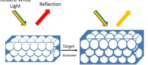
PCs have been interestingly applied to optical biosensors. The recognition of the target molecules induces changes, such as the crystal lattice or the refractive index, thus affect-ing the optical properties of the photonic structures. The responsiveness of the PC mate-rial is evaluated in terms of shifts in the wavelength of the peak reflectance and/or inten-sity variations (Figure 1). Therefore, the materials and structures of PCs allow tuning the diffracted wavelength, such as synthesis of colloidal nanoparticles with a certain size to obtain reflectance peaks at chosen wavelengths within visible light. Moreover, PCs can be integrated with electroactive polymers widening the range of applications of label-free sensing [19, 22].
Figure 1: Induced changes in the optical response of photonic crystals, such as structured colloidal silica nanoparticles, upon molecular sensing.
1.2.2 Electrochemical Biosensors
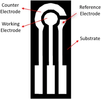
analyte concentration. The electrode surface is usually a three-electrode system (Figure 2) comprised by a working electrode (WE), a counter electrode (CE) and a reference electrode (RE). To study the behavior of the analyte at the electrode/electrolyte interface both potential and current must be monitored. To do this, the system must be disturbed out of its equilibrium, which is done by applying potential and polarizing the WE anodi-cally or cathodianodi-cally and, to apply the potential, a standard constant potential is needed, hence the RE. The CE main purpose is to complete the current circuit, since the RE cannot be used as the current carrying electrode, as its potential would change. The opposite reaction from the WE occurs in the CE, therefore whenever the WE is being reduced, the CE is being oxidized [23].
Electrochemical sensors are categorized into three groups, according to the type of signal used for biosensing applications: amperometric, impedimetric and potentiometric [22, 23].
Figure 2: Three-electrode system adapted design with increased counter electrode area.
Electrochemical Biosensor Applications
5 Impedimetric sensors measure the impedance of the system after immobilization of bi-olayers at the electrode surface. This happens when molecules present at the interface between the electrode and the electrolyte have a strong impact on the overall impedance.
When there is a change in charge-transfer resistance (RCT) between solid and liquid
inter-face, in the case of redox-active probes present in the electrolyte, the expected changes in
the RCT caused by molecular recognition or binding can then be measured [29]. This kind
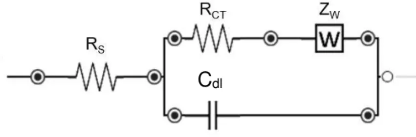
of biosensors are generally analyzed by electrochemical impedance spectroscopy, a tech-nique that applies a range of AC frequencies and measures the impedance, i.e., resistive and capacitive properties [30]. EIS not only allows to know more about formation of
double layer capacitance (Cdl), solution resistance (RS), charge transfer resistance and
diffusion transport, but also its results can be modeled by fitting with electrical equivalent circuit, such as the Randles circuit presented in Figure 3. [12]
Figure 3: Randles equivalent circuit with mixed kinetic and charge-transfer control.
1.3 Molecularly Imprinted Polymers
The synthetic solution to mimic natural antibodies relies on using inexpensive plastic materials, which enable to maintain the required selective recognition and at the same time show longer stability. Plastic antibodies are produced by molecular imprinting, a process where the template interacts with functional monomers to form high affinity recognition sites on the polymer matrix, mimicking the binding sites of natural antibodies [31]. The template has a stable polymer grown around it. After polymerization and re-moval of the template, the recognition sites are exposed and exhibit high affinity for the specific target due to complementary size, shape and chemical functionality retained in the polymer matrix. In analogy, it is a comparable procedure to the creation of a plaster cast of a hand, only on a nanoscale [30, 31].
The molecular imprinting technique must be customized considering the properties of the target analyte and the type of sensor. Some common imprinting techniques are polymer-ization with thermal or photochemical initiation, either in bulk or surface imprinting, and electropolymerization.
Considering that the molecularly imprinted polymer shall be integrated in an electro-chemical device, the chosen method is electropolymerization, since it allows the adjust-ment of several parameters that control the rate of polymer growth, thus enabling to control film thickness and morphology [28]. It also avoids the necessity for initiators. In
electropolymerization, the template is mixed with the monomer in a proper solvent and the polymeric matrix is created directly on the transducer surface by applying the required electrical conditions, making biomolecule immobilization and MIP synthesis a one-step process [34].
To create the imprinted surface binding sites, the selected monomer is of upmost im-portance, since it is essential for the success of the plastic antibodies. For detecting com-plex macromolecules like proteins, the presence of charged functional groups in mono-mers, in the pre-treated substrate prior to polymerization or on the surface of nanoparticles used in sensor design may improve protein binding [35].
Polypyrrole emerges as an excellent option to be used as the polymer in MIPs, because its deposition conditions are already well studied, as described in the literature [30, 34]. Moreover, the electropolymerization of Py may be precisely controlled, enabling to tailor the polymer film embedding the PC. The fine tuning of producing such MIP-based pho-tonic sensor retains the versatility of PCs while broadening the responsiveness of the sen-sor due to electrochemical modulation.
In the present work, Py is electropolymerized on ITO substrates containing an opal struc-ture of aminated silica NPs that shall be embedded on the polymer matrix. To construct the MIP, the template protein interacts with the charged surface of the NPs prior to Py electropolymerization. The absence/presence of the protein in the matrix changes the nanostructured layers of NPs within PPy. Therefore, protein detection based on this MIP may be evaluated both through electrochemical measurements and reflected analysis.
1.4 Transparent and Flexible Electronics
In the last years, a great interest emerged around room temperature processing of any devices that could be used for electronics, with special focus on flexible optoelectronics. Numerous papers were written about polymeric solutions and even paper to be used as substrates and the transparent conductive oxide (TCO) industry is booming. This area has been dominated by Indium Tin Oxide due to its outstanding optical and electrical prop-erties [37]. However, suitable alternatives are being investigated nowadays, owing to the increased price of indium, the need for high processing temperatures and drawbacks in flexible applications [38]. AZO is a potential candidate by being an abundant, non-toxic and low-cost material with high chemical stability. Among all doped ZnO films, AZO demonstrates the lowest resistivity and it has been proved that it upholds its good
proper-ties when deposited at room-temperature, if RF sputtering conditions are optimized [37–
39] This makes AZO suitable for flexible electronic applications.
Electrochemical Biosensor Applications
7
2
| Materials and Methods
This chapter reports the experimental techniques and methods used throughout this work. The first part reviews the fabrication of thin films. Secondly, the patterning of the elec-trodes by laser direct writing is fully explained and, lastly, the electrochemical procedures and assembly of the biosensor are described.
All chemicals employed in this thesis were of analytical grade. Aqueous solutions and washing were made with ultrapure milli-Q water.
2.1 AZO Thin Film Deposition
2.1.1 Physical Vapor Deposition – RF Sputtering
RF magnetron sputtering was used to deposit AZO thin films of about 200 nm on Corning 1737 glass and PEN at room temperature, resorting to a ceramic oxide target of
ZnO:Al2O2 (98:2 mass ratio, 99.99% purity, ø: 2 inches). All substrates were 10 cm×10
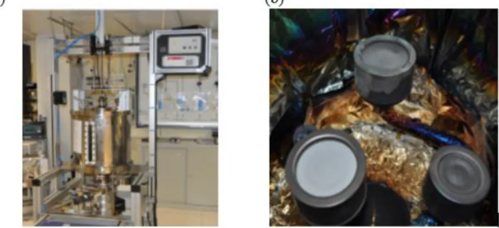
cm and ultrasonically cleaned before being loaded into the chamber for 10 min with ace-tone, isopropyl alcohol and deionized water. The RF sputtering system used for the dep-osition of AZO was a home-made system developed at CENIMAT|i3N/CEMOP, which does not have a load-lock for sample loading and removal (Figure 4). A pre-sputtering of 10 min was done to safeguard the reproducibility of the deposited thin films, since each deposition required taking the vacuum chamber to atmospheric pressure, where the
tar-get’s surface could be contaminated.
Figure 4: Home-made RF magnetron sputtering system: (a) vacuum chamber exterior; (b) vacuum cham-ber interior with 3 different magnetrons.
The processing parameters of the sputtering technique were optimized for both substrates,
considering different conditions of RF power, percentage of oxygen in the Ar+O2
mix-ture, deposition pressure and time. For glass substrates optimal depositions were obtained
with 100 W RF power, 0% oxygen in the Ar+O2 mixture and 2.0 mTorr of pressure. As
for PEN, the best parameters were 100 W RF power, 2.0 mTorr of pressure but 1x10⁻⁵
2.1.2 Rapid Thermal Annealing
Thin films produced by sputtering needed their dopants activated, therefore they were exposed to a fast heating from ambient temperature to 500 ºC, with a heating ramp of 5 ºC/s. As soon as the maximum temperature was reached, it was held for 1 min and then lastly quenched. The used equipment was an AS-One RTP system from Annealsys.
2.2 Laser Direct Writing
2.2.1 Apparatus
To pattern the chosen design of the three-electrodes configuration onto the substrates, a
pulsed CO2 infrared laser cutting system (Universal Laser System VLS 3.5) was used,
with a focal length of 50.8 mm, wavelength of 10.6 μm and 2.0” lens (focus point of 0.127
mm). The laser setup comprises a laser source, a beam delivery system and the moving stages. The latter is the only controllable subsystem, a computer interface uses an RGB
colour map that encodes specific laser power, speed and repetition rate, plus, the 2.0” lens
can be swapped for a HPDFO (High-Power Density-Focusing Optics) lens, which offers a focus point of 0.025 mm.
2.2.2 Thin Film Etching
To pattern the chosen design of the three electrodes onto the substrates, Adobe Illustrator CC 2017 was used to design the pattern as a vector image input and, since the laser system works as a printer, the chosen RGB colours are converted into specific parameters. For the metal oxides in glass substrates the laser was operated at 35 W, 1000 pulses per inch and 1.27 m/s. As for the flexible substrates the conditions were the same, except for power, which was 10 W.
2.3 Thin Films Characterization
The characterization of thin films produced was an essential part of this work to assess their properties and quality, allowing the optimization of their production techniques. Hence, the metal oxides fabricated in the first part of this thesis were electrically, optically and chemically characterized.
2.3.1 X-Ray Diffraction
X-Ray Diffraction (XRD) results were recorded using a commercial X’Pert Pro MRD
from PANalytical with a monochromatic Cu Kα (K=1.54Å) radiation source, an applied
current of 55 mA and voltage of 60 kV, in a 2Ө range from 10º to -90º using a continuous
scanning mode.
Electrochemical Biosensor Applications
9
2.3.2 UV-Visible-NIR Transmittance Spectroscopy
UV-Vis-NIR spectroscopy is a characterization technique used to assess the optical prop-erties of materials. The basic idea behind it is to measure the absorbed, transmitted or reflected light of a sample that has been illuminated by an incident light of varying wave-lengths. This spectroscopy is also useful to quantify electronic transitions, since it allows to analyze accurately at which wavelength the samples absorb light and the frequency of light is correlated to energy.
The used equipment was a Shimadzu UV-3101PC UV-VIS-NIR Spectrophotometer, with a step of 2 nm, in a range between 250 nm and 2500 nm.
2.3.3 Scanning Electron Microscopy
For obtaining a morphological and chemical analysis of the fabricated materials, a SEM Zeiss Auriga CrossBeam Workstation was used. The thin films were coated with 15-25 nm of Au/Pd and the images were taken with a 5-15 kV of accelerating voltage and a mix of SE and BSE signals.
2.3.4 Four-Point-Probe Measurements
Samples of, usually, semiconductors can have their electrical impedance measured by a simple apparatus of a four-point probe. This device uses the outer pair of probes to apply a current in the sample, while the two inner probes measure its voltage. This way, the substrate resistivity can be obtained. By having this four-point probe, with separation of current and voltage by different electrodes, this method eliminates contact resistance from the measurement, making it a more accurate one.
2.3.5 Hall-Effect Measurements
The Hall effect is a complex notion that comes from an electric current flowing through a sample in a perpendicular direction to a magnetic field, which applies a transverse force on the moving electrons, pushing them to one side of the conductor. The charges will accumulate, producing a measurable voltage between the two sides of the sample, called the Hall Voltage. Hall effect measurement systems are sophisticated instruments capable
of determining numerous material parameters, such as Hall voltage (VH), Hall coefficient
(RH), resistivity (𝜌), carrier mobility (μ) and carrier conductivity type. The used
equip-ment was a HL5500PC from BioRad.
2.3.6 Contact Profilometry
Every deposition had a small piece of substrate covered with Kapton tape, so the thickness of the film could be measured. These measurements were done with profilometer Ambios XP-Plus 200 Stylus, with a stylus tracking force of 10 mg and minimum speed of around 0.01 mm/s.
2.4 Biosensor Assay
2.4.1 Apparatus
between the electrodes and the potentiostat was acquired from DropSens (DRP-DSC4MM) but it only had sufficient height to read the PET/PEN electrodes. Therefore, for the glass substrate with three-electrodes configuration a homemade interface device was built at CENIMAT. The fabrication protocol and pictures of the interface can be consulted on Appendix A.
The optical properties of the biosensor during the several steps of fabrication and in re-sponse to target biomarker were analyzed in terms of reflectance and the spectra (190-1110 nm) were recorded on a Thermo Scientific UV-Vis spectrophotometer (Evolution 220).
2.4.2 Electrochemical Procedures
The electrochemical studies comprised cyclic voltammetry to electropolymerize the mon-omer pyrrole (Py) and electrochemical impedance spectroscopy (EIS) analysis to follow sensor construction and response. The CV scans were performed from -0.2 V to 1.0 V with a scan rate of 50 mV/s. EIS studies were made in open circuit potential using a sinusoidal potential perturbation with 0.01 V of amplitude and 50 frequency values, log-arithmically distributed over a frequency range from 0.1 Hz to 0.1 MHz. The EIS assays
were all achieved using 5.0 × 10⁻³M of [𝐹𝑒(𝐶𝑁)
6]3− and 5.0 × 10⁻³M of
[𝐹𝑒(𝐶𝑁)6]4− as redox probe, prepared in PBS buffer (10 mM, pH 7.4) The EIS data was
fitted to a Randles equivalent circuit using 2.1 Nova Software from Autolab. Every assay was ran in triplicate to rule out errors or experimental bias.
2.5 Sensing Material Assembly
2.5.1 Silica Nanoparticles Synthesis and Functionalization
The imprinted material was assembled in several stages. The first one consisted on the
sol-gel synthesis of monodispersed spherical silica (SiO2) nanoparticles through an
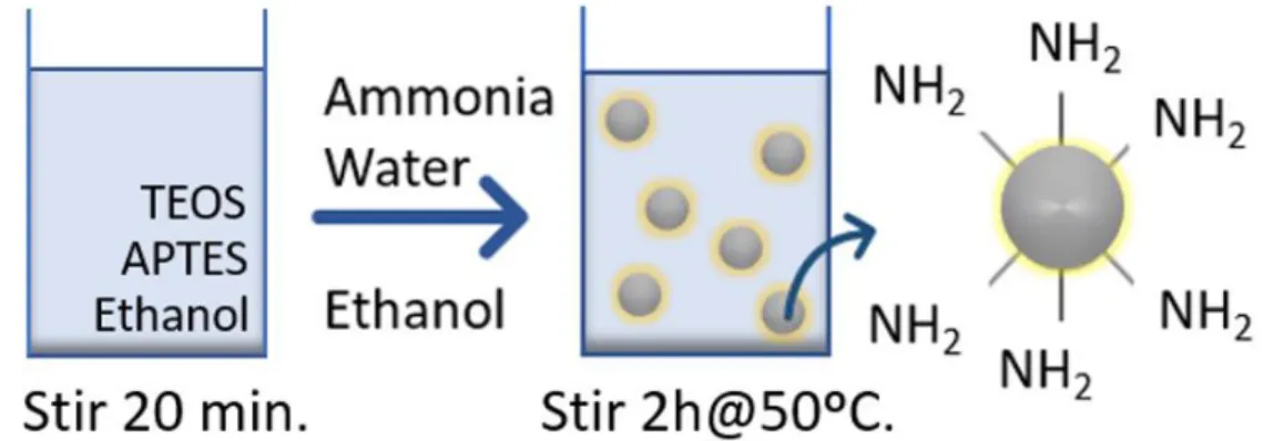
adap-tation of the Stöber method [43][44][45], which comprises the base-catalyzed hydrolysis of tetraethyl orthosilicate (TEOS) and (3-aminopropyl)triethoxylosilane (APTES) in eth-anol.
Electrochemical Biosensor Applications
11 Two separate solutions were prepared: solution A and B. Solution A was a mixture of
ethanol in the same volume as the sum of APTES and TEOS: 1.565 mL of ethanol, 49 μL
of APTES and 1.516 mL of TEOS. Solution B consisted of 2.25 mL of water, 0.828 mL of ammonia and 18.792 mL of ethanol. As shown in Figure 5, solution B was placed in a three neck round bottom flask with a Graham condenser attached, while A was put in a flask and both were mixed, at 50ºC, for 20 min. Then, solution A was slowly added to the round bottom flask, at 900 rpm. The reaction was done at 50ºC for 2h, at 300 rpm and, in the end, the round bottom flask was placed on ice, to certify that the reaction had finished.
The resulting aminated SiO2 NPs are positively charged for increased affinity towards the
highly glycosylated protein biomarker and a brief schematic of the reaction can be seen in Figure 6.
Figure 6: Schematic diagram of the synthesis of amino-functionalized SiO2 NPs with APTES and TEOS.
2.5.2 Nanoparticles Deposition
The second stage was a vertical deposition of the colloidal SiO2 NPs in order to obtain highly ordered assembled layer films. The entire chip was placed in a vial, where it stayed dipped in a solution containing 1 mg/mL of NPs, with an approximate angle of 65º for 3 days. Several vials were prepared in batches and stored in controlled conditions, at 50 ºC. To guarantee uniformity across the deposition, the WE was cleaned beforehand with Ex-tran, MiliQ water, ethanol and acetone. To remove the surplus of deposited material, NaOH 3 M was used.
2.5.3 Molecularly Imprinted Photonic Sensor Construction
The next step was to create the plastic biomarker mold. To attain it, CEA (10 µg/mL in PBS buffer 10 mM, pH 7.4) was incubated within the assembled colloidal NPs for 30
min, followed by a washing step and the electropolymerization of Py (50 × 10−3 M in
replaced by incubation with PBS buffer (10 mM, pH 7.4). All steps of MIP/NIP construc-tion were followed optically through reflectance analysis and electrochemically using EIS, as described above.
2.6 Biosensor Characterization
2.6.1 Fourier-Transform Infrared Spectroscopy
A Nicolet iS10, from Thermo Scientific, was used for infrared spectroscopy assays for chemical characterization of samples. The data was collected using an Attenuated Total Reflectance (ATR) sampling accessory equipped with a single bounce germanium
crys-tal. The spectra were acquired with 250 scans and a 4 cm-1 resolution, in the range of
4000-525 cm-1. This technique reveals the composition of materials and can be used for
identification and confirmation of produced materials.
2.6.2 Scanning Electron Microscopy
SEM studies were performed on a FEI Quanta 400FEG ESE/ Edax Genesis X4M, from Thermo Fisher Scientific, operating at high and low vacuum at 15 kV and using a SE signal. Sample preparation involved the deposition of a 15 nm AuPd thin film to ensure good electrical conductivity at the surface. SEM images were used to analyze both the
size and monodispersity of the colloidal SiO2 NPs as well as the order of opal films
as-sembled on ITO chips.
2.6.3 Analytical performance of the biosensor
The analytical performance was evaluated through the rebinding properties of the im-printed films. Calibration curves were obtained by incubating the WE with increasing concentrations of CEA (1 ng/mL to 10 ng/mL) prepared in PBS buffer (10 mM, pH 7.4). The calibration curves were analyzed electrochemically by EIS measurements and the
graphs are depicted as RCT against the logarithm of CEA concentration. Simultaneously,
Electrochemical Biosensor Applications
13
3
| Results and Discussion
Along this chapter, all relevant results obtained throughout this work are presented, dis-cussed and compared to previously published papers.
The first section, 3.1., refers to the optimization and fabrication of transparent electrodes. In the following sections, the production of a viable sensing device using ITO as proof of concept is described. Thus, section 3.2 displays the results related to the synthesis and characterization of silica nanoparticles prior to assembly of the photonic crystal. In sec-tion 3.3 all the results regarding the sensor construcsec-tion are shown and, finally, secsec-tion 3.4 presents the results obtained from sensor response studies.
3.1 Optimization, Production and Characterization of TCO’s
3.1.1 AZO Deposition Optimization
The first objective of this work was to fabricate AZO thin films with thicknesses between 100 nm and 200 nm on glass and flexible substrates that showed low electrical resistivity and high optical transmittance, simultaneously.
RF magnetron sputtering is a great technique for the deposition of transparent oxides, as it offers a large coverage, good adhesion, high film density and, most importantly, com-patibility with low or even room temperatures. Nonetheless, sputtering parameters have a strong impact on thin films quality, significantly affecting the growth and crystal struc-ture of the produced films. To optimize the fabrication process, different RF power and post-thermal treatment were tested. The target-substrate distance was kept at 15 cm for all depositions. An AZO target from Alineason Materials with 2% of Al was used to deposit all AZO thin films.
3.1.1.1 RF Power
One of the main controllable parameters on RF magnetron sputtering is the RF power, which is responsible for transferring kinetic energy to the bombarding ions that hit the target material. Higher RF powers lead to more ejected species and, in result, higher dep-osition rates that create thicker thin films.
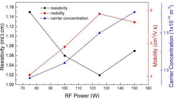
Four different RF powers were tested (75 W, 100 W, 125 W and 150 W), as shown in Figure 7, which presents the electrical characterization of the produced AZO samples.
Figure 7: Electrical resistivity, Hall mobility and carrier concentration of AZO thin films deposited for 1h, at 2 mTorr and at room temperature as a function of RF power.
The increment in RF power induces the ejected species to reach the substrate with a higher energy, allowing them to move along its surface and form little clusters. This mechanism is often observed in polycrystalline oxides, where the rise in power density favors grain growth due to the increased mobility of the ejected species. These species migrate to new positions in the crystalline lattice where its connections are optimized, supporting nucle-ation and grain growth and, consequently, higher crystallinity in the films. The increased carrier concentration is associated with less oxygen being weakly linked to the film
sur-face and the lack of O2 in the sputtering atmosphere not being able to compensate the
vacancies.
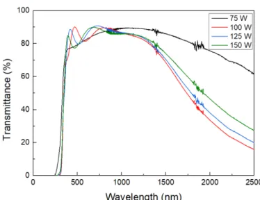
Figure 8 illustrates the optical characterization of thin films deposited with different RF powers. From the optical spectra, it is visible that the 75 W sample is not very crystalline, but all the other depositions led to highly transparent thin films in the visible range, being the lowest value of transmittance 76% in this range. In the visible spectrum, the transmit-tance decreases with the increase of RF power, but the opposite behavior is depicted in the NIR region. The highest transmittance in the visible region is from the 100W sample, although it is the lowest for higher wavelengths, which means this sample has high free carrier concentrations, since they are responsible for the photon absorption in this region [46]. Increased RF power led to higher transmittances in the NIR region, which can be related to lower bandgaps that are associated with high crystallization of the thin films. Therefore, it can be concluded that increasing the RF power of the depositions leads to a higher level of crystallization of the AZO thin films [46, 47].
Electrochemical Biosensor Applications
15 in the visible region. The electrical characterization is not the best, but bearing in mind all the variables, 100 W is a condition that guarantees good results. Increasing RF power enhances the trap probability of substitutional Al and interstitial Zn, that act as donors, leading to more efficient doping [47]. That is also justified by decreasing resistivity in function of RF power.
3.1.1.2 Rapid Thermal Annealing
To obtain the best possible conditions, a rapid thermal annealing was always performed on AZO thin films on corning glass substrates. This thermal treatment consisted in 1 mi-nute of high temperatures that ranged from 200 ºC to 600 ºC, with the purpose of dopant activation. Flexible substrates, due to being polymeric, were not compatible with this
Figure 8: Optical transmittance of AZO thin films deposited for 1h, at 2.0 mTorr, with different RF powers and no thermal treatment.
Figure 9: (a) XRD patterns of AZO thin films deposited for 1h at 100 W, 2.0 mTorr and thermally treated at different temperatures. The heating ramp was fixed at 5 ºC/s. (b) Optical transmittance of same
treatment, as the high temperatures surpassed their melting point. Figure 9a presents the XRD analysis of the different temperature conditions tested by rapid thermal annealing (RTA).
The XRD diffraction patterns of the several AZO thin films show a polycrystalline
hex-agonal wurtzite structure, with a preferential orientation along the c-axis (002),
perpen-dicular to the substrate plane, since this plane formation requires low energy [46]. Broader peaks and smaller intensities represent smaller crystallite size in materials, suggesting that higher RTA temperatures led to further crystallization of the AZO thin films. Peak posi-tion shifts towards higher angles are related with the variaposi-tions in interatomic distances, mainly due to increased dopant activation with the rise of RTA temperatures, since the thickness remained the same. The intense peak associated with the lowest RTA tempera-ture shows an unexpected behavior that can be justified by a larger area being analyzed by the x-ray beam, due to human error in the sample characterization.
The optical transmittance of the films was also inspected and measured in a wavelength from 250 nm to 2500 nm, to include also the near infrared region, as shown in Figure 9b. Each condition shows a different average transmittance in the visible range, evidencing a proportional relation between transmittance and temperature, since the lowest RTA tem-perature is associated with the lowest transmittance value and for higher temtem-peratures, the transmittance increases accordingly. From the previous XRD analysis, it was con-cluded that increased annealing temperatures led to higher crystallinity in films, therefore another conclusion can be made: the structural properties of the thin films influence their transparency in the visible region. As for the near infrared region (1500-2500 nm), the spectra seem to hint to a similar behavior, except for the 200 ºC spectrum, which shows
some incongruencies. The curve’s profile depicts a strong role of the free carrier
concen-tration, because the reduction of transmittance at longer wavelengths is a result of the absorption of photons by free carriers. Therefore, materials highly doped with free elec-trons present a much lower NIR optical transmittance [46].
Since an increase in carrier concentration leads to blockage of the lowest states in the conduction band and an increase in the optical bandgap, the analysis of this regions allows the conclusion that lower optical transmittances are associated with higher bandgaps, which in turn, are associated with a lower state of crystallization.
Electrochemical Biosensor Applications
17 The heating rate of the post-thermal annealing was also optimized and Figure 11 presents the performed characterization. Figure 11a shows the XRD analysis of three different heating rates, where it is visible that the slower rate creates more crystalline thin films, due to its more intense peak and reduced full width at half maximum. The other rates express an analogous behavior, with the exception that the 150 ºC/s ramp shows a new
peak at 2Ө = 63.2º, associated with the (226) plane of the cubic structure of Al2O3 [48].
Figure 11b illustrates the optical performance of the most relevant heating rates from XRD analysis. Slight differences are present in the visible region, where the 75 ºC/s con-dition presents higher transmittance, but, overall, optically this parameter is insignificant.
The chosen RTA condition regarding the heating ramp was 5 ºC/s, since optically all the tested conditions were identical, but the XRD data showed increased crystallinity when compared to the other samples. A maximum temperature of 500 ºC was also the selected Figure 11: Effects of RTA heating ramps on AZO thin films deposited for 1h at 100 W, 2.0 mTorr and thermally treated at 500 ºC. (a) XRD patterns of three different heating ramps (b) Optical transmittance of
relevant RTA heating ramps.
parameter, because even though an annealing of 600 ºC shows higher optical transmit-tance in the NIR region, which points towards a higher optical bandgap and crystallization of the thin films, the XRD and electrical characterization are similar to an annealing per-formed at 500 ºC.
3.1.2 Laser Parameters – Glass Substrates
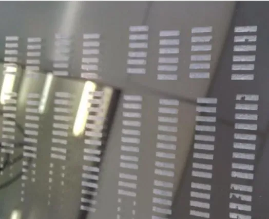
Having optimized the substrate materials, the next step was to study the effects of laser power and speed, with the objective of manufacturing electrodes with the best possible quality. To that end, a systematic study was conducted where the same ITO coated glass substrate was tested with multiple combinations of laser speeds and powers, as shown in Figure 12. The study started with ITO since it was commercial and therefore more relia-ble.
Figure 12: Photograph of the first laser test in ITO glass. Each column is associated with a fixed speed (decreasing from left to right), while each row corresponds to a fixed power (decreasing downwards).
The laser works as a printer, having a vectorial image input and moving along two axis, eroding material as it moves. In this case, the laser is used to etch the TCO thin films. A simple rectangle pattern was chosen to maximize the ITO glass substrate and the number of pulses per inch was kept at 1000, as it was not a relevant parameter for these engrav-ings. The patterns were ablated as a matrix, where each column was associated with a scanning speed and the rows corresponded to a specific laser power. The laser power was studied between 10 W and 50 W, while the laser speed varied between 0.38 m/s and 1.27 m/s. The laser interface displayed laser power and speed in a percentual scale, where 100% corresponded to the maximum power and speed achieved by the device.
Electrochemical Biosensor Applications
19 On the first case, the amount of energy that is transmitted to the ITO glass is not enough to break the chemical bonds for the occurrence of etching. When the speed decreases, the amount of energy transferred over time to the same substrate spot rises, especially in the Table 1: Results of the optimization of laser parameters in terms of power and speed. Blue stands for con-ditions with no visible effects; Yellow means the patterns were only partially etched; Green is for concon-ditions with the expected results; Red corresponds to parameters, where the glass substrate was attacked and flaked.
100 90 80
SPEED (%)
70 60 50 40 30POW
ER
(
%
)
100 90 80 70 60 50 40 30pattern edges, where the laser changes position and ends up uncontrollably dispersing thermal energy. Therefore, partial patterns result from a fusion of dispersed thermal en-ergy and increased laser power. Good pattern engraving happens when the combination of dispersed thermal energy and applied laser power over time are just enough to deteri-orate the ITO thin film, without affecting the glass substrate. This results in a fully resis-tive pattern. The last event, when substrate degradation exists, is justified by very high amounts of energy being distributed over longer periods of time to the same spot, which are also combined with increased thermal dispersion, resulting not only in the breaking of chemical bonds in the ITO thin film, but also in the glass underneath, perforating, damaging it permanently and even leading to some layers to flake, as can be seen in the last column of Figure 12.
This optimization was done at the naked eye, so an electrical characterization was needed. Four-point probe technique was used to assess if the patterns that were fully etched and did not show glass disintegration were, in fact, fully resistive. All the conditions marked as red and green in Table 1 were unable to conduct any current, therefore could not be read by the four-point probe technique, while conditions marked as yellow could be read but showed high discrepancy. As for all the conditions checked as blue, since ITO is a good conductive oxide, their electrical behavior was outstanding and homogeneous,
showing 20 Ω/square of sheet resistance.
substrate led to an increase of its temperature, resulting in thermal effects that were hard to predict.
By trial and error, the chosen laser conditions are 35 W of power and a scanning rate of
1.27 m/s. This laser speed is the system’s maximum and it was chosen to prevent any
further local thermal dispersion and even though several combinations worked, these pa-rameters guarantee a perfect pattern etching at all times. It is important to mention the infrared laser leads to a higher absorption coefficient of ITO, helping the etching process, but also increasing the thermal effects. This could be reversed by using an UV laser as an alternative.
The same parameters were tested on the AZO glass substrates and the results were very similar, so the optimal laser conditions for this material remain the same.
3.1.3 Laser Parameters – Flexible Substrates
The laser parameters for etching PET substrates had already been optimized by another researcher in CENIMAT, therefore those conditions were the first to be tested on the ITO on PET electrodes. Power was set to 10W and speed was 1.27 m/s and these conditions worked perfectly, eroding the layer of oxide from the polymeric substrate. Since PET, while transparent in the visible range, shows a light yellowish tone, it makes the absorp-tion of energy coming from the laser to be higher, making its surface more prone to etch-ing. These facts are sustained by Figure 13, which shows the optical transmittance of ITO on both glass and PET.
Figure 13: Optical transmittance of ITO thin films deposited on glass and PET substrates.
ITO electrodes deposited on PET substrates displayed a sheet resistance of 35 Ω/square
and it remained the same after laser direct writing.
3.1.4 ITO Electrodes
Electrochemical Biosensor Applications
21 Figure 14a shows a SEM image of a region on the ITO surface where a laser patterning has been done. The surface is smooth with some scratches, which are probably waste from the laser etching and the area where material has been removed is clearly visible.
Figure 14: EDS analysis of an ITO electrode. (a) SEM image of the region in which the EDS was carried out. (b) EDS mapping of both elements. (c) EDS mapping of indium. (d) EDS mapping of tin.
Figure 14b is an EDS image of the combination of the analyzed elements and it proves that ITO has indeed been removed in that region, as a visible lack of indium and tin can be observed. Figure 14c,d reinforce this evidence, as they represent the distribution of each element and, again, the right section of the images are clearly poorer in indium and tin.
Since the objective was to obtain a silica photonic crystal film on the ITO electrodes, these were also characterized in terms of reflectance as a control. Figure 15 illustrates the reflectance of a clean electrode on the visible region.
Figure 15: Optical reflectance of unmodified ITO coated glass electrodes.
3.1.5 AZO Electrodes
AZO substrates after being patterned by laser direct writing displayed the same electrical properties already shown above and their optical transmittance remained alike, although due to equipment limitations the measurements showed lower values. Primary electro-chemical assays on AZO electrodes displayed a very inconsistent response, since AZO can is highly susceptible to humidity, therefore aqueous solutions did not react very well with these electrodes. Further studies would be needed to guarantee a reliable behavior from AZO to this biosensing application, so since ITO was a better, more reliable and the go-to material when it comes to transparent electronics, AZO was optimized but not used as proof-of-concept for the biosensing application of this dissertation.
3.2 Nanoparticles Synthesis and Characterization
Electrochemical Biosensor Applications
23
The amino-functionalized silica NPs (SiO2-NH2) show more affinity towards the
bi-omarker, since CEA is a protein heavily glycosylated that shows a negative global charge in physiological medium. The choice of using colloidal silica nanoparticles was related to a facile synthetic route, prone to adaptations and not requiring the use of toxic organic solvents.
The sol-gel method was optimized to produce spherical, uniform, porous and monodis-perse silica nanoparticles of controllable size that were dismonodis-persed in water. Particle size depends on the concentration of reactants, catalysts and temperature. According to the literature, opposite to reaction time, reaction temperature is inversely related to the size of the nanoparticles [44].
Figure 16 portrays SEM images of the SiO2-NH2 NPs that were taken to verify their
mor-phology and dispersion. Figure 16a,b show that the SiO2-NH2 NPs are arranged in large
agglomerates, which may be explained by back-bonding of NH2 functional groups to
si-lanols on the particle surface with consequent reduction of electrostatic repulsion [51]. Nonetheless, from Figure 16c it can be stated that the nanoparticles present a very narrow size distribution with a mean diameter of 172 ± 9 nm (n=25), further confirmed in the silica opal films (below in Figure 22a).
FTIR was used to confirm the presence of the amino groups on the surface of the silica nanoparticles, since its analysis allows identifying functional groups of samples. Figure 17 shows the FTIR spectra of silica nanoparticles synthesized without and with APTES in the formulation.
Figure 16: SEM images of powdered SiO2-NH2 NPs: (a) 2000x zoom, (b) 25 000x zoom and (c)
Figure 17: FTIR spectra of silica NPs with and without amino functionalization. The inset graph corre-sponds to a magnification of the spectra between 4000 cm-1 and 1500 cm-1.
Both spectra present similar features: the intense peak at 1074 cm-1 can be associated with
the asymmetric stretching vibrations of Si–O–Si with a shoulder around 1200 cm-1. Also
related to symmetric Si-O-Si stretching vibrations are the bands found around 955 cm-1
and 795 cm-1 [52]. The broad band present around 2500-3600 cm-1 accounts for the Si–
OH stretching vibrations [44]. Then, comparing the spectra from both types of NPs, some
differences can be observed. The amino modified NPs show a weak band at 1526 cm-1
justified by the N–H vibrations of the –NH2 groups and also at 2988 cm-1 and 2900 cm-1
assigned to C-H vibrations of the –CH2 groups [42]. Overall, it can be concluded that the
functionalization with amine groups from APTES was effective.
3.3 Biosensor Construction
Before the construction of MIP materials, several parameters and conditions needed to be studied and adjusted. Therefore, the first steps are considered optimization of experi-mental variables. It must be remarked that pH is also a very important parameter, but it was always kept equal to 7.4 by using PBS buffer in all experiments, for being a similar value to biological fluids.
3.3.1 ITO Coated Glass Electrodes Characterization
Electrochemical Biosensor Applications
25 After cleaning the electrodes as described in 2.5.2, CV and EIS scans were done, as shown in Figure 18. By interpreting the CV scan in Figure 18a, it is possible to identify oxidation and reduction peaks at -0.08 V and 0.1 V and from a current point of view, the system
shows a quasi-reversible behavior, since the peaks currents are very similar, one being
-0.10 mA and the other being 0.11 mA.
Peak separation is 180 mV, therefore the redox reaction of the clean ITO electrode is quasi-reversible, because a reversible reaction has only one electron involved in the re-action, making the expected value to be 59 mV. Figure 18b presents the EIS data that was fitted to the Randles equivalent circuit in order to extract the reference value of the charge
transfer resistance, which is 259 Ω.
3.3.2 Polymerization Conditions
Throughout the construction procedure of the biosensors, one of the most impactful stages in terms of electrochemical response is the electropolymerization of Py. Consequently, the effect of PPy on the ITO coated glass substrates must be studied and the first step is to identify the potential that is necessary to apply on the electrodes so that the Py oxidation occurs in the WE surface. This result is presented in Figure 19 and the graph shows that Figure 18: Electrochemical analysis of unmodified ITO coated glass electrodes: (a) CV and (b) EIS. The
CV assay was performed from -0.7 V to 0.7 V (3 scans), with a scan rate of 50 mV/s and EIS was done with an amplitude of 0.01 V, with a logarithmic step type and a frequency range of 0.1 Hz to 0.1 MHz.
an irreversible oxidation occurs between 0.58 V and 0.94 V, reaching its maximum at 0.75 V. This information allowed to choose an electropolymerization range from -0.2 V to 1 V that guarantees the polymerization of the monomer.
Monomer concentration is likewise one of the critical parameters, since it plays a major role in the conductivity of the polymer. Five different Py concentration values were tested: 10 mM, 30 mM, 50 mM, 70 mM and 90 mM. This study was done by electropol-ymerizing each concentration by performing 10 CV cycles at 50 mV/s and comparing the resulting EIS data of each experiment, as shown in Figure 20.
Figure 20: Comparison of EIS spectra of the resulting electropolymerization of different Py con-centrations.
The spectra behavior is as expected, showing a proportional increase in RCT as the
mon-omer concentration rises and the biggest effect on conductivity is associated with the highest polymer concentration. Comparing the spectra with the one of cleaned ITO, serv-ing as control, it is evident that all the electropolymerization attempts led to the formation of a polymeric film, considering that all concentrations present changes in the sensing surface. MIP materials present a challenge concerning the equilibrium between monomer concentration and distribution of recognition sites throughout the sensing surface. Thus, the decision surrounding the best concentration value relies on several parameters, such as the need of an intense measurable signal that proves the formation of PPy, the necessity of keeping a conductive interface and growing a polymeric layer with just enough thick-ness to guarantee a structure capable of integrating the NPs and creating proper imprinted cavities, without creating a diffusional barrier to allow a good sensor sensitivity. Taking all this into account, the concentration of 50 mM was chosen as optimal.
Electrochemical Biosensor Applications
27 of effective recognition sites. The CEA molecules may lay deep within the polymeric film surface, thus decreasing both the chances of a successful template removal as well as good subsequent recognition. On the other hand, a low number of cycles may not in-duce the formation of a PPy film with proper recognition cavities.
A study about the number of CV cycles was performed and a comparison was made be-tween a chip before electropolymerization and chips where Py 50 mM was polymerized using 5 and 10 cycles, as depicted in Figure 21. Higher number of CV scans were assayed, but their EIS data was discarded due to lack of stabilization in the readings.
Figure 21: Comparison of EIS spectra of the resulting electropolymerization of Py 50 mM with different CV cycles.
By fitting the EIS spectra into a Randles equivalent circuit, it was assessed that the RCT
value for 5 and 10 cycles is 1220 Ω and 1355Ω, respectively. So, 5 cycles was the chosen
condition because it showed good stabilization and less resistivity when compared to 10 cycles, which will create a more penetrable matrix and therefore a more sensitive device.
Scan rate can also influence the stability and resistance of the created polymer, however a value of 50 mV/s was selected right away, since literature proved it to be the best in similar conditions to this type of application [32], [36]. These works performed a study to pick the best solvent to remove the protein after the polymerization stage without dam-aging the polymeric matrix. Based on those results, oxalic acid (0.5 M) was selected as it did not demonstrate significant interference with the WE surface [34, 36].