2010
João Corujo Branco
Malaquias
Filmes finos de Cu
2ZnSnS
4para PV:Comparação de
métodos de crescimento
Cu
2ZnSnS
4thin films for PV: Comparison of two
growth methods
João Corujo Branco
Malaquias
Filmes finos de Cu
2ZnSnS
4para PV:Comparação de
métodos de crescimento
Dissertação apresentada à Universidade de Aveiro para cumprimento dos requisitos necessários à obtenção do grau de Mestre em Engenharia Física, realizada sob a orientação científica do Dr. António Ferreira da Cunha, Professor Auxiliar do Departamento de Física da Universidade de Aveiro
o júri
presidente Prof. Dr. João de Lemos Pinto
professor catedrático do Departamento de Física da Universidade de Aveiro
Prof. Dr. Hugo Águas
professor auxiliar do Departamento de Ciência dos Materiais da Faculdade de Ciências e Tecnologia da Universidade Nova de Lisboa
Prof. Dr. António Ferreira da Cunha
acknowledgements I’ll start by thanking my Supervisor, Professor António F. da Cunha for giving me the opportunity to perform this work and for all his teachings. I would also like to thank my laboratory colleagues for all their support and healthy conversations as well as everyone who is connected to FISUA.
Acknowledgements are in order to everyone at the Helmholtz Centre, in Berlin, who contributed to my work.
Finally, I would like to address special thanks to my colleagues Inês Carvalho and Luís Brito and especially to all my family and friends.
keywords Thin Films, Cu2ZnSnS4, absorber layer, solar cell
abstract This work focuses on a comparison between Cu2ZnSnS4 thin films with
precursors grown exclusively by evaporation or by evaporation and RF Magnetron Sputtering. On the films which were grown using the second method was either sputtered ZnS or elemental Zinc. The morphology and composition of the samples was studied by SEM/EDS and their structure by XRD.
Both methods were successful in producing thin films containing Cu2ZnSnS4.
The samples which had their precursors grown exclusively through evaporation exhibited the most compact morphology but also were the ones that had more undesirable crystalline phases. Regarding the remaining samples, in the case where elemental Zinc was sputtered no diffusion issues were observed, whereas the ones with ZnS presented a layer of this material on the surface. This report is divided into six chapters which contain the introduction, information relative to semiconductors, Cu2ZnSnS4 solar cells, the growth and
characterization techniques, the experimental procedure, results and their analysis and ends with the conclusion.
palavras-chave Filmes finos, Cu2ZnSnS4, camada absorvente, célula solar
resumo Com o presente trabalho pretende-se efectuar uma comparação entre filmes finos de Cu2ZnSnS4 cujos precursores foram crescidos exclusivamente por
evaporação ou por evaporação e pulverização catódica RF com magnetrão. A morfologia e composição das amostras foram estudadas por SEM/EDS e a sua estrutura por DRX.
Com ambos os métodos conseguiu-se crescer filmes finos de Cu2ZnSnS4. As
amostras cujos precursores foram crescidos exclusivamente através de evaporação apresentavam uma morfologia mais compacta, contudo eram as que apresentavam maior número de fases cristalinas indesejadas. Relativamente às restantes amostras, no caso em que Zinco foi depositado por pulverização catódica, não foram observados problemas de difusão, contudo o mesmo não se verificou para as que continham ZnS, sendo que estas apresentavam uma camada deste material na superfície dos filmes.
Este documento encontra-se dividido em seis capítulos que incluem a introdução, informação relativa a semicondutores, células solares de Cu2ZnSnS4, as técnicas de crescimento e caracterização, o procedimento
João Corujo Branco Malaquias Index
1. Introduction ……….……… 1
1.1 Motivation …..……… 1
1.2 State of the Art and Objectives ...………... 2
2. Basics of Solar Cells …...………..……… 3
2.1. PN Junctions and Solar Cells ...………..….………..………... 3
2.1.1 Equilibrium Situation ..……….………..……….. 3
2.1.2 Non-Equilibrium Situation .………..…..……….…. 4
2.1.3 Photovoltaic Effect ..………...……….. 4
2.1.4 Electrical Parameters of a Solar Cell ...……….…..………. 5
2.2. CZTS Solar Cell ……….………..…… 6
2.2.1 Cell Structure and Band Alignment …..………. 6
2.2.2 Substrate ……….……….. 9
2.2.3 Molybdenum Back contact ……….. 9
2.2.4 CZTS Absorber Layer ………..……… 9
2.2.5 CdS Buffer Layer ….……….……… 10
2.2.6 Undoped ZnO ……….……….. 11
2.2.7 Transparent Conducting Oxide …….………. 11
2.2.8 Nickel/Aluminium Electric Contacts ………..………. 13
3. CZTS Growth and Characterization Techniques ……….……… 14
3.1 Sputtering ……….………. 14
3.2 Vacuum Evaporation ………..………. 15
3.3 Sulphurization System ………. 16
3.4 Comparison Between Sputtering and Vacuum Evaporation ………...……….. 16
3.5 X-Ray Diffraction ………..……… 17
3.6 Scanning Electron Microscopy and Energy Dispersive Spectroscopy ……… 19
4. CZTS Growth Details...……….………. 21
4.1 Evaporation of Binary Precursors ……….………. 21
4.2 1st Sulphurization and Thermal Annealing ……….……….. 22
4.3 Sputtering Deposition ………...………... 24
4.3.1 Zinc Target ……….………...……... 24
4.3.2 Zinc Sulphide Target ………..………...………. 25
4.4 2nd Sulphurization and Thermal Annealing ………..………..…. 26
5. Results and Discussion ………...………. 26
5.1 Binary Precursors ………...………... 26
5.2 Series 1644 ……….………..… 29
5.3 Series 1705 ……….………..…… 33
5.3.1 1st Sulphurization ………. 33
5.3.2 2nd Sulphurization ……… 37
6. Conclusion and Future Work ………... 43
João Corujo Branco Malaquias 1
1. Introduction 1.1 Motivation
Nowadays with the increasing concern on environmental problems, the development of energy producing technologies based on renewable energy sources are gaining increased momentum. Additionally, the future depletion of fossil fuels also contributed for this sudden interest. In the last few years the deployment of PV technology has increased steadily and significantly over the world (15% in 2009) but it is still far from having a significant share in the energy market (0.66% of the total in 2007) [1] [2].
Figure 1: Installed PV power in several countries over the years [1].
This is in part due to its cost per Watt-peak which only by the end of 2008 reached a value of 1$ for thin film technology, which represents a milestone [3] [1]. That figure’s importance is related with the price of producing energy using coal (being the cheapest way of producing electricity), which costs precisely 1 $/Wp [3].
The group of PV technologies includes single and polycrystalline silicon solar cells (which still dominate the market), amorphous silicon, group III-V semiconductors, CdTe and Cu2In(1-x)GaxSe2 (CIGS); these last four are included on the group of thin films solar cells and are already available in the consumer market.
Of these, CIGS present both the most efficient laboratory cells (20.1%) and panels (12.1%, obtained by Avancis using Cu2InSe2) [4] [5]. Nonetheless, this technology cannot be expected to be irreplaceable since it has Indium in its composition, which besides being rare in the Earth’s crust it has become extremely expensive [6]. Additionally, 50% of the market was already based on recycled In in 2003 and this behaviour was expected to grow [9], which doesn’t contribute to the long-term sustainability of CIGS, even with the recent fall on demand of InP semiconductor devices.
2 João Corujo Branco Malaquias
Figure 2: On the left, a plot showing details of the Indium market. On the right, information relative to the total production of Indium [6].
Therefore, Cu2ZnSnS4 (CZTS) has risen as a cheap and more sustainable alternative. Both Zinc and Tin are cheaper and more abundant in our planet [6] [7] [8] and it also has the advantage of not using Selenium, which is hazardous for human health. Thus, developing this technology is of major importance since it may represent a viable replacement for CIGS if similar efficiencies are attained.
1.2 State of the Art and Objectives
The first paper to report a CZTS solar cell was published by K. Ito et al in 1988, there it was assessed that this material, grown by sputtering, was suitable for thin film photovoltaic applications and a device was finished, exhibiting a Voc of 165 mV [10]. Further characterization was performed in 1996 but with films produced by a spraying method [11], while in 1997 Katagiri et al finished some solar cells by growing the absorber layer by electron beam evaporation but obtaining poor results (η=0.68%); the cell structure was CZTS/CdS/ZnO/Al [12]. In 1997, T. Friedlmeier et al grew CZTS thin films by co-evaporation, observing Tin-loss for temperatures above 450 ºC and concluding that undesirable crystalline phases should be present in the samples. Previously, the same author had finished solar cells with 2% of conversion efficiency [13].
Over the last years, some groups have continued to study CZTS, growing it by different approaches, as well as characterizing the respective solar cells. Moriya et al through 2005-2008 carried out his study with photo-chemical growth methods and pulsed LASER deposition. For the first method, experimental results were improved by annealing on a N2+H2S atmosphere and obtaining efficiencies up to 1.74% for the latter [14] [15] [16] [17]. By the same time, T. Tanaka et al opted for hybrid sputtering (DC/RF Sputtering + evaporation) and co-evaporation, being successful in growing CZTS with both techniques and finding that despite the good optical, electrical and structural properties for PV applications, the last two greatly depended on the amount of Copper [18] [19] [20]. Other chemical-based growing methods have been used by K. Tanaka and N. Kamoun between 2006 and 2008, with the first resorting to a sol-gel method whilst the second to spray pyrolysis; both of them were successful in growing CZTS [21] [22] [23]. Cheaper electro-chemical methods were used by J. Scragg and A. Ennaoui, the two of them accomplished the desired objective, with the latter one obtaining a maximum efficiency of 3.6% [24] [25] [26].
Other processing options are the sequential evaporation of stacked metallic precursors performed by H. Araki (2008), the evaporation of binary precursors by A. Weber (2009) and the RF Sputtered binary precursors by J. Seol (2003); conversion efficiencies reported in these works were up to 1.79% [27] [28] [29].
Finally, Katagiri et al are the most successful group related with this technology, using electron beam co-evaporation and co-sputtering. They currently hold the efficiency record of 6.74%, which was obtained by resorting to the latter deposition system, in 2008. More information on these authors’ work can be found on references [30] [31] [32] [33].
Nonetheless, it is noticeable that even though this material is being properly studied for at least ten years, progress wasn’t significant. This happens because some fundamental properties of CZTS aren’t accurately known and no interface studies have been conducted so far. Summing up, all these factors hinder
João Corujo Branco Malaquias 3
not only the growth stage of the material but also the way how the devices are finalized. Some of these matters will be explained in other sequences of this thesis.
This work’s aim is to grow CZTS from a different and unattempted approach. The main features of this growth method are the incorporation of metallic Zinc or Zinc Sulphide through RF Magnetron Sputtering on Cu-Sn-S (CTS) thin films grown by evaporation and thermally anneal them in order to form CZTS. Characterization will be made after every step of the process and compare the resulting samples with the ones grown by the common evaporation method involving three binary precursors.
Furthermore, it’s also an objective to understand the physics behind the solar cell, as well as the purpose of each layer by which it is composed.
2. Basics of Solar Cells
2.1 PN Junctions and Solar Cells
2.1.1 Equilibrium Situation
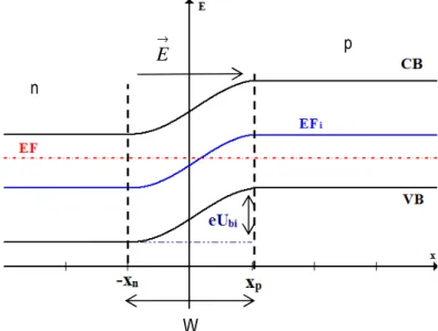
If two semiconductors, one p-type and the other n-type, are connected to each other a pn junction is formed. As in all physical phenomena, equilibrium has to be reached so as soon as the junction is formed a majority carrier migration begins due to the carrier concentration gradient: the electrons on the n-type will diffuse to the p region and the holes of the p-type semiconductor will diffuse to the n-region [34]. This leaves ionised donors on the n side and ionised acceptors on the p side, which induce the creation of an electric field, E, that opposes the described diffusion movement to the point that it comes to an halt [34]. This whole process results in the formation of a space charge region – width W –, with insulating characteristics, since there are no free charges [34].
Finally, as theory dictates, a change in charge carrier concentration causes an adjustment of the distance between the bands and the Fermi level – which has to be constant along the junction in this situation – causing a bending of the first ones across the depletion region as the following figure shows; thereby the majority carriers will always “see” a barrier when moving through the junction [34]. This barrier is what gives the pn junction the rectifying behaviour that a diode exhibits: the particles must have certain amount of energy in order to pass that “obstacle”.
Figure 3: PN junction in equilibrium.
W
→
E
n
4 João Corujo Branco Malaquias
2.1.2 Non-Equilibrium Situation
When voltage is supplied to a pn junction there are modifications to the built-in potential barrier and to the width of the depletion region (since there is a new electrical field to add to the existing one). These changes depend on how that voltage is applied: if the positive potential is connected to the p zone (direct bias) then both those variables shall decrease, on the opposite situation (reverse bias) their value shall increase [34]. Another consequence of this action is the alteration of the Fermi level, which is no longer constant and is divided in two, denominated quasi-Fermi Levels: one for holes and the other for electrons [34].
The following figures represent the band diagrams for these situations.
Figure 4: On the left: PN junction under forward bias. On the right: PN junction under reverse bias.
One should notice the relative position between the quasi-Fermi levels: under forward bias they get closer to the bands, which means there is an excess of majority carriers while under reverse bias the opposite occurs, thereby there are less particles capable of moving. Finally, by changing the potential barrier one is tuning the ability to let current flow: with a forward bias almost every particle has sufficient energy to cross the barrier, while under reverse bias nearly zero carriers have that capacity.
2.1.3 Photovoltaic Effect
The photovoltaic effect occurs when an electron is separated from the covalent bonds, which assure the integrity of the semiconductor, through the absorption of photons by a zero-biased pn junction in equilibrium. These electrons shall diffuse through the junction, generating a voltage, until they recombine with a hole. Obviously, the usefulness of this effect lies in the usage of the photogenerated electrons to power a circuit.
As referred, this effect is dependent on the absorption of photons so it is demanded that these particles must have energy equal or superior than the band gap. Despite this is a quantum phenomenon, where a photon generates an electron, thus being expected a one to one relation, in practical terms this rarely happens since there may be reflections, absorption by other layers of the solar cell or it may even happen that a generated electron immediately relaxes and re-bonds with the atom [35].
W n p W n p
João Corujo Branco Malaquias 5
2.1.4 Electrical Parameters of a Solar Cell
In order to evaluate the performance of a solar cell one has to consider its I-V characteristic (figure 5) which, due to the cell’s structure, is similar to one of a pn junction; thus exhibiting a rectifying behaviour [36].
Figure 5: IV curve of a solar cell.
By analysing the referred curve, one easily concludes that the region of operation, or region of interest, is the fourth quadrant where current is being supplied to the load.
On an ideal solar cell under illumination, the measured current is simply the sum of the photocurrent, IL, (which is generated by exciting excess charge carriers with solar radiation) with the junction’s dark current; thereby being described by the following equation [36]:
L B s
I
T
K
qV
I
I
−
−
=
exp
1
(1)One can extract four parameters from the I-V curve related with a solar cell’s electrical performance [36]:
1) Voc – Open Circuit Voltage – It is proportional to the band gap energy and is negatively influenced by increasing temperature due to the exponential dependence of the saturation current.
2) Isc – Short Circuit Current – It corresponds to the generated photocurrent and is positively influenced by a temperature increase since minority carrier diffusion increases, but in a less pronounced way when compared to Voc.
3) Vm, Im – Maximum voltage and maximum current, respectively – From these two parameters the maximum power point, Pm, can be determined.
In order to evaluate to a full extent the electrical performance, one must calculate, using the referred parameters, both the efficiency, η, and fill factor, FF. The first represents the ratio between the obtained electrical power and the incident electromagnetic power and has an ideal value of 31% for a band gap energy of 1.4 eV; the latter is related with the form of the shaded area in figure 5, the higher FF value the closer the shaded area is to its maximum value, Voc.Isc. Relating the fill factor with a temperature increase, one can expect it to diminish since the Voc decreases as previously referred; this FF reduction also has a negative
6 João Corujo Branco Malaquias
impact on the efficiency as mathematically proven afterwards. Both can be determined using the following equations [36]: sc oc m m I V V I FF ⋅ ⋅ = (2) optical sc oc optical m m P I V FF P I V ⋅ ⋅ = ⋅ =
η
(3)The following figure represents the electric equivalent of a solar cell:
Figure 6: Solar Cell equivalent circuit.
The circuit includes a current source which represents the photocurrent generated by the incident radiation, a diode representing the junction, the resistance Rp is the shunt resistance and it’s related with leakage currents and theoretically should have an infinite value [36], while Rs is the series resistance, which ideally should be zero, being responsible for losses at the surface and across the cell [36] [37].
Concerning cell degradation, the series resistance plays a much bigger role than the shunt resistance and mainly affects the fill factor]. Furthermore, with these considerations equation 1 is altered to [36]:
(
S)
Sh S RS S LIR
V
KT
q
R
I
I
V
I
I
I
−
=
+
−
−
+
1
ln
(4)Finally, for a real solar cell the thermal voltage term is divided by the ideality factor, which has values between 1 and 2 and is related with recombination currents and defect currents. Obviously, cell efficiency decreases with increasing ideality factor.
2.2 CZTS Solar Cell
2.2.1 Cell Structure and Band Alignment
The structure of the CZTS solar cell still hasn’t been target of major improvements since there are a considerable number of issues related with the growth of the absorber layer, thereby it is based on the CIGS cell structure (which can be found on reference [38]). Still, current state of the art CZTS solar cells (produced by Katagiri et al) are constituted by SLG/Mo/CZTS/CdS/ZnO:Al, thus eliminating the intrinsic ZnO layer from
João Corujo Branco Malaquias 7
beneath the transparent conducting oxide (TCO) [32]. The following figure summarizes this information, considering the full structure.
Nickel/Aluminium Grid
TCO: ZnO:Al / In2O3:Sn – 350 nm i-Zno – 50 nm
CdS Buffer Layer – 70 nm
Absorber Layer: CZTS – 2.2 µm
Molybdenum Back contact – 1 µm
Substrate: Soda Lime Glass
Figure 7: CZTS solar cell structure.
This lack of study generated a major flaw in our knowledge of this device since the band alignment in the CdS/CZTS interface is not known. This means that there may be a certain number of effects that could influence the electric parameters that aren’t known. One example of these phenomena is the creation of an inversion layer in CIGS near the interface between CIGS/CdS [38].
Nevertheless, using theoretical data relative to electron affinities and each material’s band gap one can attempt to predict how the bands shall bend on the CdS/CZTS interface. Still, in order to do it one should first observe the diagrams in figure 8 and 9, which were drawn based on the information present in references [39] [40]; where A is the work function, χ is the electron affinity and Eg is the band gap.
Figure 8: Band diagram for CdS.
eV 8 . 3 1 =
χ
A1 eV Eg =2.4 CdS8 João Corujo Branco Malaquias
Figure 9: Band diagram for CZTS.
Because the values for A depend on the experimental conditions (relative position between the Fermi Level and the closest band), further calculations shall be performed based only on the electron affinity. Nonetheless, to simplify the process one has to consider that for CZTS the Fermi level will always be as close to the valence band as possible and that for CdS the same relation is verified but for the conduction band. Thereby, under these conditions, A1 will have a lower value than A2. Furthermore, by applying Anderson’s rule [41] and aligning the vacuum levels one concludes that it is a type I heterojunction, thus the following equations are valid and it is possible do determine the band offset [39] [41]:
CdS CZTS c E =
χ
−χ
∆ (5)(
CZTS)
g CdS g CZTS CdS V E E E = − + − ∆χ
χ
(6)Table 1 summarizes the discussed information:
Table 1: Determined band offsets and constants related with CdS and CZTS.
Material Eg/eV χ/eV ∆Ec /eV ∆Ev /eV
CdS 2.4 3.80
CZTS 1.5 4.58
0.78 0.12
Although the determined offsets don’t offer any information on how the bands shall curve, they at least indicate that there will be some type of energy displacement. Still, from references [41] [34], one may expect that either a spike will appear on the conduction band and a cliff on the valence band or a cliff in both bands (figure 9).
The scenario presented in figure 10 a), is similar as the one observed in CIGS, which is beneficial since the potential barrier “seen” by both electrons and holes helps reducing recombination at the interface [42]. As for the second hypothesis, in figure 10 b), electrical losses should be hindered since no potential barrier is present but changes in recombination mechanisms can’t be predicted. Nonetheless, accurate band bending calculations are still needed; this can be achieved by solving the Poisson equation with the adequate continuity equations. eV 58 . 4 2= χ A2 eV Eg=1.5 CZTS
João Corujo Branco Malaquias 9
Figure 10: Band bending prediction with a) a spike in the conduction band and a cliff on the valence band and b) a cliff in both bands. 2.2.2 Substrate
The substrate provides mechanical support for the cell and thereby it is demanded that it must withstand the entire processing, its thermal expansion coefficients must be similar to the ones of the subsequent layers and it mustn’t be reactive. Additionally, it is believed to be important that the substrate – in this case Soda Lime Glass – has some percentage of Sodium since it was reported that for CIGS it may improve its general efficiency, enhance p-type conductivity [38], improve surface morphology and crystallinity [43]. Despite this, a similar study still hasn’t been conducted for CZTS.
2.2.3 Molybdenum Back Contact
In the substrate configuration the first layer to be deposited is the Molybdenum back electric contact. Ideally, this layer should have low resistance and should form an ohmic contact with the absorber layer (this matter is still subject of some discussion since some groups report it should form a Schottky contact) [44]. The main feature of this material (and other refractory metals) is that with it one can obtain simultaneously a layer with good adhesion and low sheet resistance [45]. This is achieved through sputter deposition at different pressures: at low pressures the deposited films are under compressive stress, since the sputtered material suffers fewer collisions and arrives with higher energy at the substrate thereby the resulting film will have a more compact structure which results in lower resistances; while at higher pressure the film is under tensile stress due to the higher number of collisions that the material suffers thus forming a more porous surface which contributes positively to a higher adhesion [45].
This fact changed the growth method of this layer, nowadays most research groups use the bi-layer method: they first deposit a high-adhesion layer and over it one with low resistivity, thereby obtaining one layer with both features.
There are also other requirements it must obey to: it mustn’t react with the absorber layer, it must be permeable to sodium from the substrate and be highly reflective.
2.2.4 CZTS Absorber Layer
CZTS is a semiconductor which exhibits p-type conductivity and a direct band gap between 1.45 and 1.66 eV [25] which is very close to the ideal value of 1.4 eV [38]. It crystallizes in the Kesterite structure [46] (figure 11 a)) which belongs to the space group I4 (tetragonal), with theoretical lattice parameters approximately a= 5.46 Å and c= 10.92 Å [47], still there have been reported some structural modifications; the most common is the one where CZTS is formed with the Stannite (figure 11 b)) structure – space group I42m, tetragonal system [47]. The difference between these structures lies on the alternation of cation layers: in kesterite this alternation happens between CuSn and CuZn, while in stannite is between Cu2 and ZnSn [47]. Still, it’s difficult to distinguish between these two phases: on one hand Cu and Zn have similar atomic weights, on the other hand both these structures have very similar lattice parameters [47]. Its absorption coefficient is approximately 105 cm-1 [25] being somewhat lower than the one for CIGS [43].
c E ∆ c E ∆ 1 χ 2 χ 1 A 2 A E x V E ∆ a) b) 1 χ 1 A 2 χ 2 A V E ∆ E x
10 João Corujo Branco Malaquias
Figure 11 – a) Kesterite structure and b) Stannite structure (adapted) [47].
One limitation concerning the growth of this material is the current lack of thermodynamic information; thereby the optimal growth conditions aren’t established which means that during the experimental work spurious phases like ZnS, CuxS or SnS2 appear [48] which obviously degrade the quality of the final film.
Furthermore, characterization of these samples isn’t always straightforward, for instance, it’s very difficult to distinguish ZnS from CZTS through XRD and simultaneously it can be difficult to assess the non-existence of ZnS through Raman Spectroscopy [49]. Some thermodynamical data is present in reference [48]. Nonetheless some authors claim that the main chemical reaction path to form CZTS is through Cu2SnS3 and ZnS, according to the following equation [50]:
4 2
3
2SnS ZnS Cu ZnSnS
Cu + → (7)
Another important aspect is related with stoichiometry, currently the CZTS record cells have the following atomic ratios Cu/(Sn+Zn) = 0.85, Zn/Sn = 1.25 and S/(Cu+Sn+Zn) = 1.10 [32] instead of being stoichiometric. This fact can be related with defect physics, for instance a copper poor film can enhance the p-type behaviour, as well as a copper-rich/zinc-poor one; still the best combination is still a copper-poor/zinc-rich due to compensating phenomena but it has the disadvantage of promoting the formation of the referred spurious phases [51].
2.2.5 CdS Buffer Layer
This layer constitutes the n region of the junction. Besides its obvious function, it’s also fit for protecting the absorber layer from the upcoming deposition processes [38] and to diminish recombination at the CZTS/CdS interface [22] by smoothing its surface and through defect passivation. The growth process (usually chemical bath deposition) of this layer requires optimization, since for extremely thin surfaces no pn junction is formed but if the layer is too thick then some parameters start to suffer degradation [52] [22] – for CZTS the highest efficiency was obtained for a 70 nm layer [32]. To better understand this discussion, in figure 12 a) one can observe that the Voc increases with increasing thickness, as for the Isc in figure 12 b) initially there is an increase of this parameter but for a deposition time of 25 minutes degradation is observed; the FF variation is shown in figure 12 c) and its behaviour is similar to the one described for Isc,; regarding figure 12 d), it shows that the efficiency increases steadily for the lower deposition times and decreases for a 25 minute deposition time. For these solar cells the explanation for such findings still have no physical explanation, nonetheless it may be similar to what happens in CIGS where there is a diffusion of Cd2+ ions into the surface of the absorber layer thus forming a buried pn junction [22].
João Corujo Branco Malaquias 11
Figure 12: Variation of a solar cell’s a) open-circuit voltage, b) short-circuit current density, c) fill factor and d) efficiency with CdS deposition time [52].
Although the best performing single junction thin-film solar cells are produced with a CdS buffer layer [53], some work has been performed with CIGS in order to replace this layer by one which doesn’t use toxic elements [54] and without degrading cell performance. Success in this area is highly desirable since it would turn the CZTS solar cells environmentally friendly and wouldn’t be prejudicial for society.
2.2.6 Undoped ZnO
There have not been any studies about the impact of this layer on the general performance of a CZTS solar cell and neither can it be slightly predicted since the band alignment for this device wasn’t calculated as referred earlier. Thereby it is necessary to resort to the studies made with CIGS. These indicate that i-ZnO enhances Voc by approximately 20-40 mV. Although the exact mechanism by which that effect comes about is unknown, one model suggests that the resistance generated by this layer reduces the negative effects of recombination currents at grain boundaries or at shunts (due to the materials’ inhomogeneities) thus limiting electrical losses [55]. Another model dictates that the i-ZnO layer helps covering the areas where CdS wasn’t properly deposited, thus preventing short-circuits between the absorber layer and the front electric contact, which would imply a large band gap discontinuity, hindering the open-circuit voltage [56].
2.2.7 Transparent Conducting Oxide
The function of this layer is, as its name indicates, to allow all wavelengths beneath cut-off wavelength to be transmitted till the absorber layer and at the same time allow electrical conduction to the contact grid [57], thereby a correct relation between absorption and resistance must be achieved [38]. The currently most used material for this window layer is ZnO:Al (AZO) since it represents a cheaper and more abundant alternative to the very efficient and still highly used In2O3:Sn (ITO) [57]; exhibiting both a n-type conductivity [58]. One conduction mechanism for these materials is related with oxygen vacancies that donate free electrons to the conduction band (which are metal-like); information related to other conduction mechanisms can be found on reference [59].
Concerning AZO, its electrical and optical properties can vary with annealing temperature, Al doping percentage or O2 flux during deposition; for instance from figures 13a) and b) one can conclude that resistivity
12 João Corujo Branco Malaquias
decreases with higher annealing temperatures due to an improved crystallinity; however it diminishes with increasing oxygen incorporation since this parameter is related to the number of oxygen vacancies; concerning carrier concentration and mobility, they have an inverse relation with the resistivity, thereby they present higher values for increasing annealing temperatures and lower ones for higher oxygen incorporation [60] [61] [62] [34].
Figure 13: Variation of the Resistivity, Carrier concentration and mobility in ZnO:Al with a) Annealing Temperature [60] b) O2 flow rate
(adapted) [61].
Tables 2 and 3 summarize the variation of the properties of AZO and ITO, respectively, with different variables.
Table 2: Variation AZO’s properties with certain variables.
Parameter Comments Reference
% Al
- Resistivity decreases with increasing doping concentration
[62]
Annealing Temperature
- Hall mobility increases with annealing temperature
[60] a)
João Corujo Branco Malaquias 13
Table 3: Variation of ITO’s properties with certain variables.
Parameter Comments Reference
% Sn
- Resistivity decreases with %Sn until a certain value and then restarts rising [64] Annealing Temperature - Doesn’t influence transmission in the visible region of the EM Spectrum
- Resistivity decreases with the increase of annealing temperature
[63]
%O2
- Transmission in the visible region of the EM spectrum increases with an increase in the %O2 - Resistivity decreases
with the reduction of the %O2
[63]
Additionally, one should note that both optical and electrical properties of both AZO and ITO are also related with film thickness; usually a thicker layer has better conductivity but worse transmission. This happens because with increased thickness there is an improvement in the surface’s morphology, thus the charge carriers won’t recombine so easily; but at the same time, there are more atoms to absorb radiation
Usually these layers are grown by Magnetron Sputtering, Pulsed Laser Deposition or Chemical Vapour Deposition [59].
2.2.8 Nickel/Aluminium Electric contacts
These contacts have the function of extracting the photo-generated electrons from the surface of the cell and “deliver” them to an external load [65].
These electrodes are constituted by two different materials, being the first one nickel, to prevent the formation of Al2O3 – which is an insulator – by contact with the window layer [65].
The geometry of these electrodes require optimization processes, since they cannot fully cover the surface nor can they occupy a small fraction of it, therefore the preferred geometry is a finger-like one, which maximizes light absorption and current extraction [65].
- Carrier concentration increases with annealing temperature - Resistivity diminishes with annealing temperature - Transparency increases with annealing temperature %O2 - Higher O2% implies lower carrier mobility and concentration - Lower O2% implies
lower resistivity
14 João Corujo Branco Malaquias
3. CZTS Growth and Characterization Techniques
3.1 Sputtering
Sputtering is a type of physical vapour deposition (PVD) techniques and it is defined as the bombardment of a solid surface (called target) with particles (usually accelerated ions from a plasma) causing, due to collisions, the backscattering of its constituent atoms [66].
The sputter process itself is purely based on linear momentum conservation: the ions collide with the atoms from the target, momentum transference occurs ejecting them from it; nonetheless this is a simplistic view of the phenomenon since there more variables to be considered, such as the ion incidence angle or the emission of secondary electrons from the target (which improves general ionization efficiency, thus contributing to the sputter rate) [66] [67]. Still, a more detailed discussion shall not be made since it isn’t the aim of this work.
In practical terms, in order to start the sputtering process one needs an environment filled with a gas, a cathode connected to the solid material that one wishes to sputter (the target) and, on the opposite position, the anode linked to the sample holder. By applying a voltage between the two electrodes the gas will ionize, being attracted to the target and colliding with it, spraying material backwards [66] [67]. The described configuration can be used either vertically or horizontally. Mainly, the ionized gas should be inert, such as Argon, so it doesn’t react with the deposited material; still if one decides to deposit an oxide, for instance, a mixture of a non-reactive gas with oxygen is an option – this variant is called Reactive Sputtering.
In general it can be considered to exist two main variants of sputtering: DC and RF, the acronyms refer to the power source type. The first can only be used when a conductive material is used as target, otherwise as ions collide with the target it will become positively charged and the process will come to an end while the latter came as a solution for the first’s limitation. By using a radio-frequency voltage and a capacitive arrangement, the polarization of the target changes over time attracting ions or electrons to its surface; but due to the inertial difference between these two particles, with the electron being lighter, the average target polarization is negative during the process, thus preventing it from ending [67]. This is shown in figure 14.
Thereby one can use RF sputtering to grow thin films of either insulating or conductive materials [67]; nonetheless the deposition rates are usually lower for RF sputtering [67].
Figure 14: The RF sputtering target’s electrical potential over time [66].
In general, three parameters influence the deposition rate of this process:
Electric Current – This variable is related to the number of ionized particles, with its increase one would observe higher deposition rates.
Voltage [68] – This parameter controls the particle’s energy. This means that with a higher voltage the ion will collide with the target with a bigger energy and thereby the sputter yield (defined as the number of sputtered atoms per incident ion, weighted by the influence of secondary electron emission [66]) will increase in most cases.
João Corujo Branco Malaquias 15
Pressure [68] – This parameter does not exhibit a direct relation with the deposition rate, instead it requires a compromise. For very low gas pressures there won’t be enough particles to initiate the glow discharge but for very high ones the mean free pass has a small value thus causing a decrease in the sputter rate. The plot in figure 15 illustrates for a general situation how the referred conciliation should occur.
Figure 15: Variation of the sputter deposition rate with Argon pressure [68] (adapted).
If one places a magnetron adjacent to the target – Magnetron Sputtering – one can “trap” the electrons into a limited region of space, performing a helical movement near the target, shown in figure 16, thus increasing the general efficiency of the process as well as the sputter rate but reducing the lifetime of the target [66].
Figure 16 – Planar Magnetron DC sputtering source [69]. Note that a magnetron can also be coupled to an RF Sputtering system. This technique was used to incorporate Zinc and Zinc Sulphide onto some of the samples grown during the execution of this work.
3.2 Vacuum Evaporation
One can evaporate a material, in vacuum, if its temperature is increased until the corresponding vapour pressure is equal or higher than the existing atmospheric pressure. From that point on, the atoms that constitute the source shall leave it and move to a surface where they can condense or adhere to.
Concerning experimental apparatus, there are various ways of achieving vacuum evaporation: through resistive heating or electron beam heating, for instance, and within these categories exist numerous geometries such as the simultaneous usage of multiple evaporation sources – co-evaporation.
The main components of an evaporation system are the source heater and the substrate holder. So, the first has to deliver sufficient thermal energy in order to allow the source to get to its vapour pressure and hold that point, it mustn’t react with the evaporated material and it should have a low vapour pressure. As for the second, it is important that it can withstand low pressures and high temperatures (if the sample needs to be heated). Moreover, both components shouldn’t be affected by any type of gas existent within the chamber.
16 João Corujo Branco Malaquias
As for the experimental parameters, generally, they are as follows [67]:
1 – Source Temperature – This parameter obviously controls the evaporation rate directly, hence the deposition rate. Still, in an indirect manner it also influences the incorporation of impurities originating from the ambient gas (it decreases with the increase of the deposition rate), morphology, intrinsic crystal structure, resistivity and stress.
2 – Substrate Temperature – This variable controls atom mobility on the surface of the substrate, typically a higher temperature facilitates material diffusion through the sample. It also influences the properties mentioned in 1.
3 – Gas pressure – The pressure of a gas, during evaporation, mainly influences sample purity and crystalline structure. Still, in some occasions, one can take advantage of its reactive properties to, for instance, form oxides.
In this work, sequential evaporation of compounds was performed in order to grow the precursor layers for the samples.
3.3 Sulphurization System
For the executed work, the incorporation of Sulphur onto the samples was performed in a tubular furnace. This type of oven is obviously distinguished by its tubular form, where the sample is placed on its centre in order to be completely surrounded by the furnace heater; as for the evaporation source, it is located on one of the extremities. Upon heating, the evaporated material is then transported, with the help of a gas flux by pressure difference. Figure 17 illustrates the described schematic:
Figure 17: A schematic of the tubular furnace used in this work [70].
In this process one can control the heating profiles for the furnace and evaporator heaters, as well as the type of gas which is introduced into the chamber and its flow rate.
3.4 Comparison Between Vacuum Evaporation and Sputtering
Since evaporation and sputtering are two very important techniques nowadays it is reasonable to establish a comparison between both of them. In general, the first produces the best results, whilst the second is the best option for an industrial environment.
The main advantages of sputter deposition are the obtainment of a uniform deposition profile even for large and complex surfaces – facilitating an hypothetical up scaling process – ,the possibility of using any material as target (whether it is an insulator, a conductor, an alloy, refractive metal, etc…) – unlike evaporation where heat-decomposing materials cannot be used –, the stability, in time, of the sputter rate is much higher opposing to what happens in evaporation in which one has to control the temperature in order do
João Corujo Branco Malaquias 17
maintain the same evaporation rate and films grown through sputtering have higher adhesion. As for its disadvantages one can remark the lower deposition rates, the increased difficulty of finding a relation between deposition parameters and film’s properties and the stress induced by the large inclusion of gas.
About evaporation it remains to be said that it is a fairly cheap technique when applied to research purposes.
One should note that many of the referred limitations for both methods can be overcome, nonetheless that would imply a higher cost and complexity as well as new problems [67].
3.5 X-Ray Diffraction
X-ray Diffraction is one of the most common techniques of analysing a sample’s crystal structure, with the utmost advantage of being a non-destructive procedure [71].
From a theoretical point of view one can look at this subject from two different ways: the one formulated by Laue or the one built by the Braggs.
The first one states that a crystal is composed by lines of atoms (in all 3 axis) that function as scattering centres. Thereby in order to observe the characteristic peaks of a certain plane in a diffractogram, constructive interference must occur – which implies that the path difference between scattered beams must be an integral number of the wavelength. With this condition established, three equations – one per dimension – can be written; additionally it should be noted that the vectors, which represent the diffracted beams, form a cone around each axis (figure 18), so in practice one observes diffraction in the directions where the three cones intersect each other [72].
Figure 18: Laue cones representing the directions of three diffracted beams with dissimilar path differences [72].
As for the Bragg approach, though being simpler it isn’t physically accurate since it’s based on the reflexion of radiation by planes of atoms which interfere constructively thus producing the maxima observed in the x-ray spectra. Still, from a geometrical point of view it produces a correct result and it delivers a simple equation [72]:
λ
θ
n dhklsin( )= 2 (8)Where dhkl is the distance between planes described by the (hkl) Miller indexes, θ is half of the deflection angle, n is the diffraction order and λ is the wavelength. This is the most practical approach.
Another structural property that can be determined through XRD analyses is the crystallite size, t, by means of the Scherrer equation, which is as follows [72]:
18 João Corujo Branco Malaquias
( )
θ
λ
cos 9 . 0 B t≅ (9)Where B is the Full Width at Half Maximum (FWHM), θ is half of the deflection angle and λ is the wavelength. This is possible, because there is a strict relationship between the diffraction curve width and crystal size. Moreover, for the experimental situations faced during this work demand that equation 7 should be multiplied by 4/3 – this is a correction related to the form of the crystallites.
In laboratory environment, the experimental apparatus used to analyse thin films are the Seeman-Bohlin and the Bragg-Brentano ones (figure 19). The difference between them resides on the detection method: the first is set for incoming radiation from angles different than the incidence angle whilst the second is set for radiation that is scattered in the same angle as the incident beam. This means that with the Seeman-Bohlin geometry one can measure planes that are tilted relatively to the specimen plane and with the Bragg-Brentano one it is possible to evaluate planes that are parallel to the specimen [71].
Figure 19: On the left: Bragg-Brentano configuration. On the right: Seeman-Bohlin configuration [71].
From an XRD diffractogram one can also assess if the material has any preferential orientations, i. e., if the crystallites are aligned on a certain direction [73]. This can be done by comparing the peak intensities of the analysed material and the corresponding powder (which is considered to have random orientation); thus if a major difference is observed between them, then there is a preferred alignment [73]. As an alternative to a powder diffractogram, a calculated theoretical spectrum can perform the same function [73]. This was done using the software Carine Crystallography and it is presented in figure 20.
João Corujo Branco Malaquias 19
Figure 20: Theoretical XRD difractogram for Cu2ZnSnS4
In this work, XRD was used to assess the existence of CZTS in samples, as well as to determine if any spurious phases (such as Cu2-xS are present).
3.6 Scanning Electron Microscopy and Energy Dispersive Spectroscopy
If an electron beam collides with the surface of a sample different types of phenomena occur, such as the emission of x-rays, cathodoluminescence or the emission of Auger electrons; these can then be used to gather electrical or compositional information of the sample. Figure 21 shows the possible interactions [72].
Figure 21: Phenomena that may occur when an electron beam interacts with a material [72].
Through collection of backscattered and secondarily emitted electrons it is possible, by amplification of the signal, to obtain an “image” of the surface of the sample. This is the main concept behind Scanning Electron Microscopy (SEM), of course that in practical terms besides the electron beam generator and the detectors there has to be the focusing and aperture systems; which for this particular device are much more
(112) (101) (103) (200)/(004) (202) (211)/(211) − (204)/(220) (312)/(116) (224) Intensity (%) 2 θ (°) 1415 20 25 30 35 40 45 50 55 60 0 10 20 30 40 50 60 70 80 90 100
20 João Corujo Branco Malaquias
complex than for the standard optical microscope. Besides the obvious advantage of the increased amplification power which allows one to analyse morphology at a nanoscale, the different phenomena that occur due to the interaction with the electrons allow the SEM to perform a varied array of analysis. One of those techniques is Energy Dispersive Spectroscopy (EDS) and it is based on the detection of X-rays emitted by the sample, from which composition information can be retrieved. The origin of these x-rays is related with the ejection of an electron from the inner orbitals of an atom and the following relaxation of another, this is illustrated in figure 22 [72]:
Figure 22: An electron ionising an atom a) and the consequent relaxation with the emission of an x-ray photon b) [72]. Since the separation between energy levels is exclusive for every atomic species, the x-rays’ wavelength is also characteristic, thereby from their detection one can fairly distinguish different elements that compose the sample – except for light elements].
Still, since the information obtained is not absolute, in order to correctly analyse the results one has to calculate atomic ratios, thus obtaining the stoichiometry of the material. A detail that one has to pay attention is the interaction volume of the electrons, since it’s not isotropic and may not include the entire volume of the sample. This fact may produce certain unexpected results. Figure 23 shows how the interaction volume may look like in reality [72]:
Figure 23: Electron trajectories inside a material after colliding with it calculated by a Monte Carlo method. This exhibits the anisotropic behaviour of the interaction volume [72].
João Corujo Branco Malaquias 21
4. CZTS Growth Details
The experimental part associated to this work involved two sets of samples: group 1644 and 1705. The first one includes samples 1644-76;78 and the second one consists of samples 1705-58;59;61;62;65. The main difference between the two sets is the type of precursors, in series 1644 they consist of evaporated SnS2, ZnS and CuS whilst set 1705 doesn’t have ZnS. Thereby the samples will have to be processed differently, according to the following steps:
1 – Evaporation of the binary precursors: This phase was performed at the Helmholtz Zentrum Berlin and consisted on the deposition of CuS, and SnS2 for set 1705, added of ZnS for series 1644. The known details of this process shall be presented. Additionally, from this information it will be determined the amount of Zinc necessary to guarantee a Zn/Sn ratio of 1.2 and Cu/(Sn+Zn) of 0.9.
2 – 1st Sulphurization: This step’s main aim is to promote the formation of CTS and CZTS by supplying enough Sulphur and energy to the sample. The chosen heating profiles shall be presented and explained. This is the final step for set 1644.
3 – Sputter Deposition: At this point, on half of the samples, from set 1705, is incorporated Zinc and on the other half Zinc Sulphide. This phase includes preliminary depositions to calibrate the targets and since no characterization methods are required, thickness results will be presented in this section.
4 – 2nd Sulphurization: This is the final processing procedure and its aim is to form CZTS, minimizing Sulphur and Zinc losses. Heating profiles are shown and discussed.
It should be noted that different pieces of a sample have the same reference, being only followed by a colon and a number. Furthermore, after each step some samples shall be characterized, but not all of them to prevent damage or contamination. Characterization means included SEM/EDS, XRD and ICP-MS (Inductively Coupled Plasma Mass Spectroscopy) results for the precursors will also be presented.
4.1 Evaporation of Binary Precursors
As referred earlier, this growth process was performed at the Helmholtz Zentrum Berlin, thereby only a limited amount of information is known, which is displayed in Table 4. ZnS wasn’t deposited on series 1705. Table 4: Experimental data relative to the evaporation of the binary precursors.
Precursor Thickness /nm Mass/ g.cm-2 x 10⁻⁴ Deposition time /min Evaporation Temperature /ºC p/mbar x 10-5 Cu/(Sn+Zn) Zn/Sn SnS2 810.6 3.6479 28.31 Sn: 1222/1202 S: 195/500/200 1.9 CuS 807.0 3.7796 12.28 1400/1355 1.9 ZnS 573.3 2.3333 19.50 ZnS: 980/960 S: 195/500/200 1.5 0.9 1.2
One should note that the indicated thickness figures are the desired ones and may differ from the real values. That is due to the fact that even after a system calibration (unavailable data), which delivers the deposition time, slight variations may occur. The evaporation sequence is ZnS/SnS2/CuS.
22 João Corujo Branco Malaquias
From the quantity values for SnS2 and CuS one can determine the quantity of zinc to be sputtered on phase 3. Thus, considering m the mass, M the atomic mass of the corresponding atom or compound, ρ the density, NA the Avogadro number and the following calculations one can determine that value:
1st – Determination of the number of molecules, N, of CuS and SnS 2. 2 18
/
10
3310
.
2
molecules
cm
N
M
N
m
N
CuS CuS A CuS CuS⇔
=
⋅
⋅
=
2 18/
10
2011
.
1
2 2 2 2N
molecules
cm
M
N
m
N
SnS SnS A SnS SnS⇔
=
⋅
⋅
=
2nd – Determination of the number of atoms, N, of Cu and Sn. Due to the compounds’ stoichiometry:
2 18 2 18 / 10 2011 . 1 / 10 3310 . 2 2 atoms cm N N cm atoms N N SnS Sn CuS Cu ⋅ = = ⋅ = =
3rd – Determination of the number of zinc atoms necessary to guarantee the desired atomic ratios.
2 18 / 10 4413 . 1 2 . 1 cm atoms N N N Zn Sn Zn ⋅ = =
4th – Determination of the corresponding thickness, t.
nm
N
M
N
t
Zn A Zn Zn2
.
219
10
7=
⋅
⋅
⋅
=
ρ
4.2 1st SulphurizationThis step’s aim is to form CTS and CZTS by supplying the necessary amount of Sulphur and thermal energy. Since the objective of this work wasn’t the study of CTS formation it was chosen a single heating profile for series 1705, which previous tests revealed to be adequate for this function. However, for set 1644 that wasn’t the case and thereby different profiles were tested. All profiles are summarized in the figure 24:
João Corujo Branco Malaquias 23
Sample Profiles Comments
1644-76 0 20 40 60 80 100 120 140 60 120 180 240 300 360 420 480 540 T e m p e ra tu re / ºC Time /min Sulphur Evaporator Furnace Sample
a)
pwork = 5 mbar Tmax = 550 ºC 1644-78 0 20 40 60 80 100 120 140 60 120 180 240 300 360 420 480 540 T e m p e ra tu re / ºC Time /min Sulphur Evaporator Furnace Sample b) pwork = 5 mbar Tmax = 525 ºC Set 1705 0 20 40 60 80 100 120 140 60 120 180 240 300 360 420 480 540 T e m p e ra tu re / ºC Time /min Sulphur Evaporator Furnace Samplec)
pwork = 10 mbar Tmax: Ranging from 525 ºC to 527 ºC24 João Corujo Branco Malaquias
One should note that the final cooling steps aren’t controlled, they simply represent the point where all sources are turned off and the system is left to cool naturally. The working pressure ranged between 5 to 10 mbar (base pressure 2.5 x 10⁻³ mbar) to minimize tin losses [74] and the maximum temperature values for the set 1705 ranged between 525-527 ºC and it was used Nitrogen (N5 purity) as transport gas with a flux of 40 ml/min. As illustrated in figure 14, temperature was controlled on the Sulphur evaporator, on the furnace heater and monitored the sample (via a thermocouple).
4.3 Sputtering Deposition
On this phase a layer of zinc or Zinc Sulphide is deposited through RF Magnetron Sputtering. Prior to the main depositions some tests were performed with both targets in order to determine the deposition rate and calibrate the In situ thickness measurement system which consisted of a quartz crystal monitor (Intellemetrics IL 150; variable tcrystal); this was done using a Veeco Dektak 150 step profiler (variable tprofiler). As for the final depositions, thickness measurements using the step profiler were possible because a dummy substrate was placed next to the samples on the sample holder.
4.3.1 Zinc Target
This target’s purity is 99.995%. All depositions were performed at 2x10⁻³ mbar (being the base pressure 8x10⁻⁶ mbar). The environment was homogenised for 15 minutes with Argon (N5 purity) being introduced at 4 ml/min. To initiate the glow discharge and guarantee its stability the gas flux was increased to 24 ml/min (p=2x10⁻² mbar) after which it was reduced to 4 ml/min. The power source was set to 75 W, a 15 minute pre-sputtering was performed for the first deposition to clean the target and ensure electrical and thermal stability – for the following depositions this step was reduced to 3 minutes – a 10 minute cooling period elapsed between depositions to prevent the target from overheating. The crystal monitor’s parameters were adjusted according to zinc’s acoustic impedance and density, the tooling factor was arbitrarily set to 50. A total of eight test samples were produced, divided by two depositions. The experimental details are shown in table 5:
Table 5: Experimental data for the zinc target calibration.
Sample P/W V/V Time/min tcrystal/nm tprofiler/nm Rate/nm.min-1
1 75 64 5 214 206 41.2 2 75 64 5 145 170 34.0 3 75 64 10 262 290 29.0 4 75 63 15 370 420 28.0 1 75 63 5 56 110 22.0 2 75 63 5 97 121 24.2 3 75 62 10 185 186 18.6 4 75 63 15 295 315 21.0
From the results one can easily conclude that time-controlled deposition isn’t entirely reliable since the deposition rate varied not only from sample to sample but also from one test run to another (being the first one less notorious); these differences could be due to voltage variation, thermal and electrical coupling differences or different surface oxidation (since from one test to another the chamber was temporarily exposed to the atmosphere). This lead to the decision of controlling the process through thickness monitoring, which had an average error of 10.6% if the first depositions were excluded (which aren’t entirely trustworthy due to the experimental apparatus) and to prolong the pre-sputtering time to 20 minutes to guarantee more stable conditions from the beginning. Table 6 contains the information of the deposition process, which was performed as described earlier:
João Corujo Branco Malaquias 25
Table 6: Experimental data relative to the zinc deposition.
Sample P/W V/V Time tcrystal/nm tprofiler/nm
1705-58 75 63 10’40’’ 226.0 270
1705-59 75 63 10’40’’ 226.0 270
1705-61:1 75 64 7’27’’ 223.5 245
1705-61:2 75 58 6’’ 220.0 220
Concerning thickness results, they are all within the referred tolerance except the ones for samples 1705-58/59. Still, the divergence isn’t relevant enough to cause a significant difference on the final results.
4.3.2 Zinc Sulphide Target
The procedure for this target is similar to the one for zinc, the only difference resides on the source power which was switched to 60 W and obviously the crystal monitor’s settings which were set in accordance with the data for ZnS and the tooling factor was changed to 20. The target’s purity is 99.99%. Additionally, a conductive elastometer was placed between the target and the magnetron to enhance electrical and thermal coupling. The test samples’ experimental results are in table 7.
Table 7: Experimental data for the ZnS target calibration.
Sample P/W V/V Time/min tcrystal/nm tprofiler/nm Rate/nm.min-1
1 60 157 15 90 123 8.2 2 60 158 15 105 97 6.5 3 60 160 30 213 230 7.7 4 60 163 45 315 300 6.7 1 60 153 15 87 98 6.5 2 60 154 15 84 93 6.2 3 60 155 30 176 156 5.2 4 60 154 45 254 243 5.4
These tests follow the same pattern as the ones for zinc, thereby it was again adopted the thickness control system, which revealed an average error of 8.6%. The probable causes for this effect were already discussed. The results for the samples are displayed in table 8.
Table 8: Experimental data relative to the ZnS deposition. * indicates the thickness measurement was performed on the periphery of the sample .
Sample P/W V/V Time tcrystal/nm tprofiler/nm
1705-62:1 60 158 1h59’ 574 500*
1705-62:2 60 158 1h59’’ 574 500*
1705-65:1 60 154 3h41’ 575 520*
1705-65:2 60 154 3h41’ 575 520*
Regarding thickness measurements, the results were bellow the expected and the correlation between the crystal monitoring and real value got worse due to unknown reasons. It should be remarked that by measuring a sample in the periphery one will obtain a lower value since in sputtering the distribution of scattered particles isn’t constant in space.
26 João Corujo Branco Malaquias
4.4 2nd Sulphurization
This is the final processing stage and its objective is to react the sputtered Zinc/Zinc Sulphide with CTS in order to form CZTS. Still, one has to guarantee that the samples receive sufficient Sulphur to make up for evaporation losses. Additionally, extra caution is required for the films which have metallic Zinc, otherwise evaporation losses will be total; thereby before increasing the sample’s temperature to higher values one must ensure that it has already received some Sulphur. Experimental conditions were as described in section 6.2 and the heating profiles are in figure 25 a).
Sample Profile Comments
1705-58;59;61 1705-62;65 0 20 40 60 80 100 120 140 160 60 120 180 240 300 360 420 480 540 T e m p e ra tu re / ºC Time /min Sulphur Evaporator Furnace Sample a) pwork =10 mbar Tmax: Ranging from 530 ºC to 531 ºC
Figure 25 a): Heating profile used on the second sulphurization for set 1705. 5. Results and Discussion
5.1 Binary Precursors
The ICP-MS results for the precursors of set 1644 are shown in table 9. The figures are related to ion concentration on a solution after diluting the sample and thereby delivering absolute values and making possible to calculate exact atomic ratios.
Table 9: ICP-MS results relative to the precursors from set 1644.
[Cu]/mol.L-1 x 10-5 [Sn] /mol.L-1 x 10-5 [Zn] /mol.L-1 x 10-5 Cu/(Sn+Zn) Zn/Sn
15.90 8.16 8.02 0.98 0.98
Bearing in mind what was stated earlier one easily concludes the following:
1 – The atomic ratios differ from the aimed ones; this means that between the system calibration and the actual deposition there were differences which lead to this variation. Both of them are approaching stoichiometry from inferior values, thus showing a zinc-poor and copper-poor film.
2 – Since on both sets were equally deposited CuS and SnS2, the concentration of Copper and Tin are the same for set 1705 and 1644. Regarding ZnS, it was only deposited on set 1644.
The SEM micrographs in figure 26 show the morphology of the precursors. Surface images and EDS mapping are only available for set 1705.
João Corujo Branco Malaquias 27 Surface Micrograph Set 1705 Cross-Section Micrograph
a)
b)
CuS
SnS
2Mo
28 João Corujo Branco Malaquias
Figure 26: SEM micrographs of the precursors for sets 1705 and 1644, respectively: a) is a surface images; b)and d) are cross-section images and c) is an EDS mapping. The precursors for set 1644 were ZnS/SnS2/CuS while for set 1705 were SnS2/CuS.
Concerning these results, the micrograph for set 1644 in figure 26 d) clearly shows the interfaces between the Mo/ZnS/SnS2/CuS layers, having these last two layers a much less compact morphology. Regarding the set 1705, its surface is shown in figure 26 a) and is somewhat compact and the grains exhibit an amorphous appearance, nonetheless one should keep in mind that it corresponds to the CuS layer. As for its cross-section, in figure 26 b), the interfaces between the different materials are visible as well as a difference in morphology. Finally, the EDS mapping, in figure 26 c) revealed the expected tendency with Copper on top and Tin closer to the bottom, still one must be critical about the Sulphur distribution since it doesn’t correspond to reality. A closer look at the mapping image indicates the existence of Sulphur where Molybdenum should be found, this is due to the impossibility of the equipment to distinguish between the photon energies of both elements as shown in figure 27.
EDS Mapping Set 1644 Cross-Section Micrograph
![Figure 1: Installed PV power in several countries over the years [1].](https://thumb-eu.123doks.com/thumbv2/123dok_br/16022327.1104297/8.892.127.745.325.629/figure-installed-pv-power-countries-years.webp)


![Figure 11 – a) Kesterite structure and b) Stannite structure (adapted) [47].](https://thumb-eu.123doks.com/thumbv2/123dok_br/16022327.1104297/17.892.226.641.147.404/figure-kesterite-structure-b-stannite-structure-adapted.webp)
![Figure 12: Variation of a solar cell’s a) open-circuit voltage, b) short-circuit current density, c) fill factor and d) efficiency with CdS deposition time [52]](https://thumb-eu.123doks.com/thumbv2/123dok_br/16022327.1104297/18.892.340.568.132.495/figure-variation-circuit-voltage-circuit-current-efficiency-deposition.webp)
![Figure 13: Variation of the Resistivity, Carrier concentration and mobility in ZnO:Al with a) Annealing Temperature [60] b) O 2 flow rate (adapted) [61]](https://thumb-eu.123doks.com/thumbv2/123dok_br/16022327.1104297/19.892.142.706.241.844/figure-variation-resistivity-carrier-concentration-mobility-annealing-temperature.webp)
![Figure 16 – Planar Magnetron DC sputtering source [69]. Note that a magnetron can also be coupled to an RF Sputtering system](https://thumb-eu.123doks.com/thumbv2/123dok_br/16022327.1104297/22.892.236.681.602.776/figure-planar-magnetron-sputtering-source-magnetron-coupled-sputtering.webp)
![Figure 17: A schematic of the tubular furnace used in this work [70].](https://thumb-eu.123doks.com/thumbv2/123dok_br/16022327.1104297/23.892.131.745.623.839/figure-schematic-tubular-furnace-used-work.webp)
![Figure 18: Laue cones representing the directions of three diffracted beams with dissimilar path differences [72]](https://thumb-eu.123doks.com/thumbv2/123dok_br/16022327.1104297/24.892.265.641.560.837/figure-laue-cones-representing-directions-diffracted-dissimilar-differences.webp)
