Brazilian Journal of Physics, vol. 34, no. 2B, June, 2004 577
High-temperature Thin-catalytic Gate Devices for
Combustion Emissions Control
Shabbir A. Khan
1, Elder A. de Vasconcelos
2, Y. Hasegawa
1, and T. Katsube
1 1Departament of Information and Computer Sciences, Saitama University255 Shimo-Okubo, Saitama 338-8570, Japan
2Departamento de F´ısica, Universidade Federal de Pernambuco
Cidade Universit´aria, 50670-901 Recife, Pernambuco,Brazil
Received on 31 March, 2003
4H- and 6H-SiC Schottky diodes responding down to 5 ppm of NO and NO2 gases at temperatures up to
450o
C were fabricated. Upon exposure to gas, the forward current of the devices changes due to variations in the Schottky barrier height. For NO gas, the response follows a simple Langmuir adsorption model. Device parameters were evaluated from linear conductance/current versus conductance plots, with improved accuracy. The linearity of these plots is an indication that the devices are not being affected by interfacial oxide layers or pinning of the Fermi level. 4H-SiC devices showed slightly superior stability and sensitivity for this application.
1
Introduction
The Nitrogen oxides (NOx)are produced from the combus-tion processes, which are the typical air pollutants. NOx combines with water in the atmosphere and form nitrous acid and nitric acid, which are one of the factors that cause the acid rain. Hence, detection and emission control of toxic NOx gases, consisting of NO and NO2, is of great
impor-tance [1]. SiC-based sensors that can be used at high tem-peratures and corrosive atmospheres have been under devel-opment for that purpose. Use of catalytic metal gate SiC devices as gas sensors has been extensively investigated by several groups [2-5].
In this work, we report on the development of SiC-based Schottky diodes for detection and monitoring of con-taminating gases, specially NO, NO2and hydrocarbons for
petroleum and automobile industry, operating at high tem-peratures. Here, we will extend our previous work [7] by the inclusion of additional results in 4H-SiC diodes, response to NO2gas and brief discussions of fabrication parameters,
response mechanisms and possible directions for future re-search.
2
Experimental Details
Successful devices described in the literature have been fabricated on heavily doped substrates with an moderately doped epitaxial layer. The heavily doped substrate provides a better ohmic contact and lower series resistance. The epi-taxial layer provides a better surface quality and better con-trol of doping concentration. In this work, we also used non-epitaxial wafers to investigate the possibility of fabricating these devices at lower costs. We used n-type, non-epitaxial
6H-SiC, Si face, SiC wafer provided by Nippon Steel Com-pany as well as 4H- and 6H-SiC wafers from Cree Research with 10µm thick homo-epitaxial layer grown on the Si face. For the epitaxial diodes, bulk and epilayer were n-type; epi-layer donor concentration was 1.7x1016 cm−3 for 6H-SiC
and 1x1015cm−3for 4H-SiC.
The wafers were ultrasonically cleaned in 5-min steps in acetone, methanol, semico-clean-23 and 46% HF with a 2-min rinse in DI-water between each step. Ni was thermally evaporated to form an ohmic back contact on the C face and vacuum-annealed at 850oC for 2 min. Finally, thin Pt gate (20 nm to 40 nm thick) was deposited by sputtering in Ar gas on the Si face (100) through a metal mask to form circular gate electrodes with a diameter of 1 mm.
The gas response and electrical characteristics of the de-vices were recorded by an automatic data acquisition sys-tem while gas flow alternated between NO or NO2diluted
in synthetic air (O2: 20%, N2: 80%) and synthetic air,
con-trolled by a gas mixing station (AERA Japan Ltd., SG-7S1) with a multi-port valve. The samples were fixed onto a platinum plate by mechanical pressure inside a quartz tube of a temperature controlled furnace, connected close to the gas mixing station in order to reduce the time lag after gas switching. The time lag was within 5 to 10 seconds. I x V (current versus voltage) measurements were taken by means of Pt wires connected to the plate and to a Pt probe pressing the gate.
3
Results and Discussion
578 Shabbir A. Khanet al.
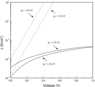
more important, even at low voltages, especially for the non-epitaxial diodes. It is necessary to take this fact into consid-eration when monitoring the forward characteristics to de-tect the effect of gas, either in constant current or constant voltage mode. This is illustrated in Fig. 1. The curves were simulated by means of the equation below, either including series resistance or not. They show the effect of a 0.1 eV decrease in barrier height on I x V characteristics.
J =Jsat h
exp³q(V−J ron)
nkT ´
−1 i
=
A∗T2exp³−qφb
kT ´ h
exp³q(V−J ron)
nkT ´
−1 i
In principle, the effect of series resistance might be alle-viated by monitoring the current of the diodes in reverse bias or by monitoring their depletion capacitance. We chose to monitor the gas response using forward bias, since reverse currents are more likely to be associated with imperfectly understood mechanisms, such as leakage and generation-recombination currents, thus bearing unclear relationship with the detection principle of catalytic gate gas sensors (barrier height changes). To monitor changes in the deple-tion capacitance is another possibility, although series re-sistance also affects the measurement of capacitance. The effect of series resistance on capacitance is less important at lower frequencies.
0,0 0,2 0,4 0,6 0,8 1,0
10-4
10-3
10-2
10-1
100
φb= 1.24 eV
φb= 1.34 eV
φb= 1.24 eV
φb= 1.34 eV
J (A/cm
2 )
Voltage (V)
Figure 1. Plot of the forward current density for an ideal SiC Schot-tky diode (dotted line) and the same diode with a series resistance of 42Ω.cm2 (solid line) at 350◦C showing the effect of barrier
height changes.
In our work, we have been using an improved technique for the analysis of barrier height changes from I x V char-acteristics [6][7]. As shown in Fig.1, when the effect of series resistance becomes important, the calculation of bar-rier height from conventional I x V plot becomes unreliable. A conductance divided by current (G/I) versus conductance (G) plot can be used to analyze the device characteristics. If the G/I x G plot is linear, one is assured that the series resistance (Rs), saturation current (Isat)and ideality factor
(n)of the device are voltage independent, and therefore the usual theory can be applied to the device. We have been using this method to calculate the series resistance, ideality factor and barrier height changes with improved accuracy.
The response characteristics of the devices are summa-rized in Figs.2-5. In this paper, we are going to show results obtained with epitaxial diodes only. The response of non-epitaxial diodes is similar, showing that they are, in prin-ciple, responsive to gas injection. However, barrier height changes tend to become difficult to detect due to their in-creased resistance. Fig. 2 shows typical I x V characteristics up to 450 ˚ C. The inset graph in Fig. 2 depicts the repeata-bility of the response at 40 ppm and 400 ˚ C, obtained by measuring the current at a fixed forward bias of 0.5 V. From Figs. 1 and 2, we see that, upon exposure to NO gas, the I x V characteristics shift reversibly to increased levels. It was possible to detect current variations for NO concentrations ranging from 50 ppm down to 5 ppm.
0.0 0.2 0.4 0.6 0.8 1.0 1.2 1.4 1.6 10-7
10-6
10-5 10-4
10-3
0 10 20 30 40 50 104
108 112 116 120
Time (min)
Cur
rent
(
µ
A)
NO 50 ppm Std. Air
C
u
rrent (A)
Voltage (V) 350o C
450o C
40 ppm NO in
Air in T=400o C
Figure 2. Current-voltage characteristics at elevated temperatures up to 450◦C in air (dotted line) and in 50 ppm of NO (solid line)
for a thin-Pt/4H-SiC Schottky diode. The inset graph shows cur-rent values at a fixed voltage of 0.5 V and temperature equal to 400◦C during repeated pulses of 40 ppm of NO.
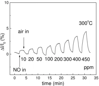
Figure 3 shows typical relative device current variations as a function of time after pulses of different gas concentra-tions for a 6H-SiC device. The graph shows the relative cur-rent variation when the atmosphere is changed between syn-thetic air and NO. ∆I is the difference between the current during gas test (I (t)) and the reference current (I0), which is
the value measured in synthetic air, just before the beginning of the test (∆I =I (t) – I0).
Brazilian Journal of Physics, vol. 34, no. 2B, June, 2004 579
0 5 10 15 20 25 30 35
0 5 10
300
oC
ppm
air in
NO in
450
400
300
200
100
50
20
10
∆
I/I
0(%)
time (min)
Figure 3. Response of a thin-Pt/6H-SiC Schottky diode to various NO concentrations. Bias fixed at +0.5 V.
0 1 2 3 4
0 1 2 3 4 5
NO ppm 450 400 300 200 100 50 20 10
∆
I/I
0(%)
time (min)
Figure 4. Gas response shown in Fig. 3 replotted using a common time origin. Time equal to zero is set to be the instant of time when the pulse of gas of different gas concentrations is injected.
0 1 2 3 4
0,0 0,2 0,4 0,6 0,8
1,0 NO ppm
450 400 300 200 100 50 20 10
time (min)
I
max
/ I
0
Figure 5. Normalized gas response using a common time origin.
The response to NO is qualitatively the same for both 4H-SiC and 6H-SiC diodes. We have found that relative de-vice current variation for 4H-SiC diode is slightly stronger than for 6H-SiC ones. We also observed that 4H-SiC devices above 400oC are more stable than 6H-SiC devices. The response depends on temperature and tends to be stronger at higher temperatures. Barrier height reduction was found to be approximately 3% for 4H-SiC and 1.8% for 6H-SiC diodes for exposure to 50 ppm of NO at 400oC. The reason for this difference is not clear. It may be related with sub-strate quality, barrier height or interface states, for example. We have found that a simple Langmuir adsorption model can adequately describe the gas response to NO. We refer the reader to our previous work, where we derive and dis-cuss this model in detail [7]. The Moreover, the linearity of the G/I x G plot is an indication that the devices are not being affected by interfacial oxide layers or pinning of the Fermi level.
We have been investigating the response of these devices to other gases, such as NO2. Fig. 6 shows a typical response
of a device to NO2. For NO2, exposure to gas makes the
barrier height to increase, whereas for NO the barrier height tends to decrease. Our experiments show that the response to NO2is more complex than for NO and further
investiga-tion is necessary to establish the correct model. It is possible that the adsorption sites for NO2have a different
polariza-tion direcpolariza-tion in comparison with NO adsorppolariza-tion sites.
0 10 20 30 40 50
12,0 12,5 13,0 13,5 14,0 14,5 15,0 15,5 16,0 16,5
Cu
rr
e
n
t (
µ
A)
Time (min)
5 10 20 40 50 100 200 ppm
Air in 2
NO2 in
Figure 6. Response of a thin-Pt/6H-SiC Schottky diode to various NO2concentrations, at 300◦C.
It is interesting to note that similar differences (barrier height increase or decrease depending on gas) were also found in experiments using Si diodes [8]. The sensing prop-erties of thin catalytic metal gate devices seem to depend in a complex way on the thickness, the structure of the film and the polarization phenomena. Various effects may oc-cur, such as reversal of voltage shifts and enhancement or decrease of gas sensitivity after gas exposure. In previous experiments in our group [8] and other groups [9], it has been observed a reversal and enhancement of voltage shift due to NO2flow when the devices were submitted to a
580 Shabbir A. Khanet al.
presence of two different kinds of NO2adsorption/reactions
on thin-Pt gates: one, which causes a positive voltage shift and another, which causes a negative voltage shift and is ac-tivated by the ammonia.
We are currently investigating the response to other gases as well as different fabrication methods of the thin-Pt gate, including laser ablation and mixtures with sensitive oxides.
4
Conclusions
We developed SiC-based NO and NO2sensitive devices
op-erating at high temperatures. Detection of NO and NO2
down to 5 ppm at temperatures up to 450 ˚ C was demon-strated. The response to NO follows a simple Langmuir ad-sorption model. The response time and recovery time do not depend on gas concentration. 4H-SiC devices have slightly superior stability and sensitivity for this application.
Acknowledgments
Authors are thankful to the financial support received from the Japanese Ministry of Education, Science Sports and Culture research grant #08455160 and from the Brazil-ian National Research Council CNPq-CTPETRO under con-tracts # 500013/01-2 and # 65.00.02.80.00.
References
[1] N. Yamazoe and G. Sakai, Trans. Inst. Elec. Jpn118-E, 60 (1998).
[2] I. Lundstr¨om, Sensors and Actuators A56, 75 (1996). [3] A. L. Spetzet al., Tech. Digest 10thInt. Conf. Solid-State
Sensors and Actuators, Sendai, Japan, June 7-10, Vol. 2, p. 946 (1999).
[4] C. K. Kimet al., Sensors and Actuators B77, 455 (2001). [5] A. L. Spetz, A. Baranzahi, P. Tobias and I. Lundstr ¨om,
Phys-ica Status Solidi (a)162, 493 (1997).
[6] J. H. Werner, Applied Physics A47, 606 (1998).
[7] S. A. Khan, E. A. de Vasconcelos, H. Uchida and T. Katsube, Sensor and Actuators B92, 181 (2003).
[8] W. Zhang, E. A. de Vasconcelos, H. Uchida, T. Katsube, T. Nakatsubo and Y. Nishioka, Trans. Inst. Elec. Jpn.118-E,614 (1998).
[9] J. Zubkans et al.,Tech. Digest 8th