JOURNAL OF NANO- AND ELECTRONIC PHYSICS Р А А - А Р
Vol. 5 No 2, 02006(3pp) (2013) Том 5 № 2, 02006(3cc) (2013)
2077-6772/2013/5(2)02006(3) 02006-1 2013 Sumy State University
Modeling of Si-QD Solar Cell in MATLAB
S.S. Bohra1, A.K. Panchal2
1 Electrical Engg. Dept. ,Sarvajanik College of Engg. and Tech., Athwalines, Surat, 390 001 Gujarat, India
2 Elect. Engg. Dept., SVNIT, Ichchhanath, Surat, 395 007 Gujarat, India
(Received 15 February 2013; published online 04 May 2013)
In this paper, the modeling and analysis of single bi-layer Si-QD solar cell is addressed. The modeling of solar cell is done in MATLAB. The photo currents are calculated for various Si-QD diameters like 2.5, 3, 3.5 and 4 nm and SiO2 barrier layer thicknesses like 2.5, 2 and 1.5 nm. It has been observed that with the Si-QD diameter, the photo-current increases. On the other hand, photo-current varies conversely with bar-rier layer thickness due low carbar-rier tunneling probability through barbar-rier.
Keywords: Quantum Dot, Si-QD, Barrier layer, Quantum Confinement Effect (QCE), Photo-current.
PACS numbers: 84.60.Jt, 81.16. – c
1. NTRODUCTION
The introduction of quantum dots application in photovoltaic devices has drawn the attention of many researchers. Reducing the cost incurred by silicon (Si) wafer is the major advantage. At the same time develop-ing high efficiency solar cells usdevelop-ing sdevelop-ingle material lim-ited by its band-gap is a difficult task. Reducing the number of steps involved in the fabrication of solar cells is also essential for cost cutting. All these challenges have motivated researchers for 3rd generation solar cells. Researchers use nano-particles or quantum dots of different materials for enhancing light absorption, charge generation, and the efficiency of solar cells. In order to reduce the overall cost of high efficiency solar cells, researchers fabricate quantum structure of di-mension less than 10 nm. The Si nano-crystals or Si quantum dots (Si-QD) of diameter less than 10 nm show quantum confinement effect (QCE). The QCE allows engineering band-gap of a material with QDs by control-ling QDs size [3]. Indeed, the quantum confinement effect manifests itself by significant modification of elec-tronic band structure of Si nanocrystals when their size is reduced to below the exciton Bohr radius (~4.9 nm) of bulk Si crystals. In particular, quantum confinement effect provokes the increasing of the effective bandgap of Si nanocrystals. Moreover, for indirect bandgap semi-conductors, like Si, geometrical confinement of carriers increases the overlap of electron and hole wave func-tions in momentum space and thus enhances the oscil-lator strength and as a consequence increases its ab-sorption coefficient. From this effect, one can expect Si nanocrystals to behave as direct bandgap semiconduc-tors. Though, the momentum conservation rule is only partially broken and Si nanocrystal strongly preserves the indirect bandgap nature of bulk Si crystals Si nanostructures are thus the perfect candidates for high-er bandgap mathigh-erials in all-Si tandem cell approach.
Carrier tunneling probability through dielectric, known as barrier layer increases as its thickness redu-ces [1]. Based on this concept very thin SiC, SiNx or SiO2 layer in superlattice (SL) can be used in the Si-QD cell. In the present modeling and simulation work, the super lattice with QDs having bandgap in the range of 1.5-2.0 eV has been introduced as intrinsic layer (i
-layer) for absorbing high energy photons [2]. QDs in a-Si layers sandwiched between dielectric layers in a super lattice structure increases its bandgap energy, which in turn should increase VOC [3].
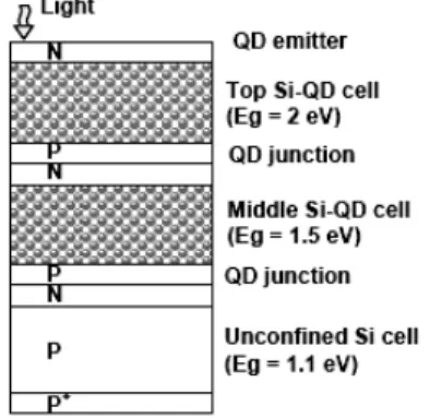
Fig. 1 –Schematic of all- Si Tandem solar cell
Ab initio calculations using density functional theory (DFT) indicate that the increasing of the optical bandgap of Si nanocrystals (or in other words quantum dots (QDs)) is expected to vary from 1.4 to 2.4 eV for a nanocrystal size of 8-2.5 nm. However, further DFT cal-culations have found that in addition to quantum con-finement effect in small QDs, the matrix has a strong influence of the resulting energy levels.
Some researchers [4, 5] have used RF magnetron sputtering to deposit alternating layers of SiO2 and SRO (Si rich oxide formed by co-sputtering Si and SiO2) of thicknesses down to 2 nm. Deposition of multilayers, consisting typically of 20-50 bi-layers, is followed by anneal in N2 ambient from 1050 to 1150 C, typically for 1 h. During annealing, the excess silicon in the SRO layer precipitates to form Si nanocrystals between the stoichiometric oxide layers, as shown in Fig. 2.
The thin multilayer structure ensures that the Si QDs are constrained in diameter by the layer thickness and a reasonably uniform size dispersion is achieved with variation within about 10 %.
S.S. BOHRA,A.K. PANCHAL J.NANO-ELECTRON.PHYS. 5, 02006 (2013)
02006-2 Fig. 2 –Schematic of Si-QD solar cell superlattice in i-layer
Fig. 3 –Bulk band alignment between crystalline silicon and its carbide, nitride and oxide, the band gap increases for quan-tum confined Si dots of 3 nm diameter to 1.73 eV
height of this barrier. Si3N4 and SiC give lower barriers than SiO2 allowing larger dot spacing for a given tun-neling current.
2. ALGORITHM
The steps involved in modeling of Si-QD solar cell in MATLAB are as shown below:
The number of photons corresponding to wave-length, from 280 nm to 1200 nm is read from excel file [9];
As shown in Fig. 4 the average Si QD diameter in-creases as the O/Si ratio is decreased from 1.3 to 0.86. The Si QDs are approximately 4 nm in the SiO0.86/SiO2, 3 nm in SiO1.0/SiO2 and 2.5 nm in SiO1.3/SiO2. The measured optical absorption of these samples is shown in Fig. 5.
Fig. 5 –Si QD diameter as a function of O/Si ratio in annealed SiOx/SiO2 multilayer films [5, 6]
For given range of , absorption co-efficient, is read. The value of for different dot sizes like 2.5, 3, 4 nm [4] have already been computed beforehand and stored in separate excel worksheet.
Find absorptance and from it find number of photons absorbed in silicon QD layer.
As barrier layer of SiO2 is sandwiched between two consecutive layers of Si-QD, carrier tunneling is to be
considered to find effective number of carriers tunneled through barrier layer. Hence, tunneling probability is computed for given (E0 – E), i.e. from 2 eV, 1.75 eV, 1.65 eV and 1.5 eV to 3.2 eV for QD sizes of 2.5, 3, 3.5 and 4 nm respectively. Some researcher [11] has came up with a simple generalised analytic model describing the size-effective bandgap (EQD) for the lowest energy states for 3D confinement:
2 2 2
2
3.6 e 2
QD bulk
q
E E smallerterms
d d (1)
Where, Ebulk is the bulk bandgap, ε is the silicon die-lectric constant taken to be 11.7, is the reduced mass of the electron-hole pair, and d is the nanocrystal diam-eter.
Fig. 6 – Room temperature absorption co-efficient of annealed SiOx / SiO2 multilayer [4], [6]
The probability that a carrier will tunnel through a dielectric can be expressed as follows:
0 2
2 ( )
16 exp 2 t
m E E
T W (2)
where, Tt Tunneling probability, m* effective mass of electron, E0 Barrier height, E Energy of carrier,
Planck’s constant and W barrier thickness[4]. From expression (1) it is understood that reducing barrier width or dielectric thickness increases tunneling probability. The difference term between conduction band edges of SiO2 layer and Si-QD (E0 – E) can be cal-culated by using expression given below:
2
, ,
0
2
g SiO g Si QD
E E
E E (3)
where, Eg,SiO2 Conduction band edge of Silicon Oxide
and Eg,Si-QD Conduction band edge of Silicon quantum dot [7]. For example by substituting the values
Eg,SiO2 9 eV and Eg,Si-QD Eopt,Si-QD 2.6 eV in expres-sion (3), we get E0 – E ≈ 3.2 eV. As the bandgap of i -layer increases, the cell’s VOC is expected to increase significantly [8-11]:
MODELING OF SI-QDSOLAR CELL IN MATLAB J.NANO-ELECTRON.PHYS. 5, 02006 (2013)
02006-3 Photo current for single layer of Si-QD and barrier layer is found by integrating carriers available at the surface of the cell.
J0 is assumed to be 9.6 10– 9 mA/cm2
VOC is found from the standard expression given below:
0
ln sc 1 OC
J nkT V
q J (4)
3. RESULTS AND DISCUSSION
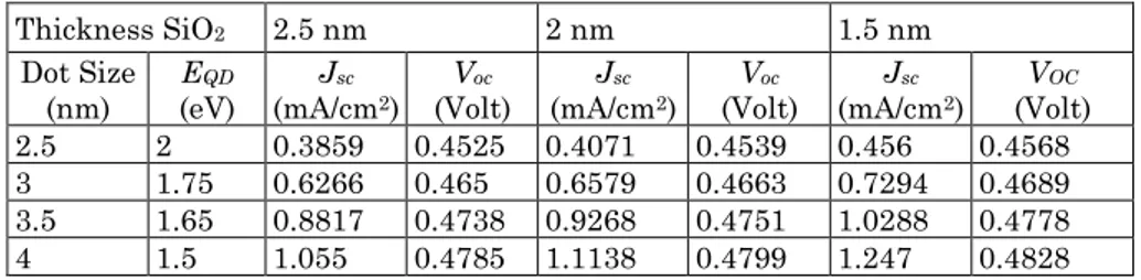
As shown in Table 1 modeling of Si-QD solar cell is done for single bilayer of SiO2 and SRO. In order to analyse the dependency of dot diameter on the photo-current, various dot sizes are chosen like 2.5, 3, 3.5 and 4 nm with different barrier layer thicknesses like 1.5, 2, 2.5 nm. It is clear from the results that the short-circuit current Jsc for 2.5 nm dot diameter (EQD 2 eV) is 0.3859 mA/cm2 for 2.5 nm barrier layer thickness, whereas, for 4 nm dot diameter Jsc has been increased to 1.247 mA/cm2 for 1.5 nm barrier layer thickness. Open circuit voltage VOC is varying with dot size and inversely with barrier layer thickness.
Table 1– Description of the special paragraph styles
Thickness SiO2 2.5 nm 2 nm 1.5 nm
Dot Size (nm)
EQD (eV)
Jsc (mA/cm2)
Voc (Volt)
Jsc (mA/cm2)
Voc (Volt)
Jsc (mA/cm2)
VOC (Volt) 2.5 2 0.3859 0.4525 0.4071 0.4539 0.456 0.4568 3 1.75 0.6266 0.465 0.6579 0.4663 0.7294 0.4689 3.5 1.65 0.8817 0.4738 0.9268 0.4751 1.0288 0.4778 4 1.5 1.055 0.4785 1.1138 0.4799 1.247 0.4828
4. CONCLUSIONS
In this work the single layer Si-QD solar cell has been modeled and simulated for wavelength 280 nm to 1200 nm. The model has been simulated for various dot sizes like 2.5, 3, 3.5 and 4 nm and various barrier layer thicknesses like 2.5, 2 and 1.5 nm. From the results, it has been concluded that as the dot size increases the QCE decreases and the optical band-gap approached towards bulk Si material i.e. 1.124 eV from 2 eV, 1.75,
1.65 and 1.5 eV for Si-QD sizes of 2.5, 3, 3.5 and 4 nm respectively. The Jsc is found to increase from 0.3859 mA/cm2 to 1.055 mA/cm2 for 2.5 nm dot size to 4 nm for barrier layer thickness of 2.5 nm. On the other hand, the Jsc also increases with reduction in barrier layer thickness, i.e. from 1.055 mA/cm2 for 2.5 nm thick barrier layer to 1.247 mA/cm2 for 1.5 thick barrier layer.
REFERENCES
1. P.S.M. Sze, Physics of Semiconductor Devices, 2nd Ed.
(John Wiley & Sons Inc.: 2007).
2. Tae-Wook Kim, Chang-hee Cho, Baek-Hyun Kim, Appl.
Phys. Lett. 88, 123102 (2006).
3. V. Vinciguerra, G. Franzo, F. Priolo, F. Iacona, J. Appl.
Phys.87, 8165 (2000).
4. Gavin Conibeer, Ivan Perez-Wurfl, Xiaojing Hao, Dawei Di, Dong Lin, Nanoscale Res. Lett.7, 193 (2012).
5. Gavin Conibeer, et al., Prog. Photovoltaics: Res. Appl.19, 813 (2011).
6. X.J. Hao A.P. Podhorodecki, Y.S. Shen, G. Zatryb, J. Misiewicz, M.A. Greenet, Nanotechnology20, 485703 (2009).
7. Kavita Surana, University of Grenoble, France, Thesis (2011).
8. Dawei Di, Heli Xu, Ivan Perez-Wurfl, Martin A. Green, Gavin Conibeer, Prog. Photovoltaics: Res. Appl. (2011). 9. D. Kovalev, H. Polisski, G. Koch, phys. status solidi (b)
215, 871 (1999).
10.Nae-Man Park, Chel-Jong Choi, Tae-Yeon Seong, Seong-Ju Park, Phys. Rev. Lett.86, 1355 (2001).
11.Pramila Mahala, Sanjay Kumar Behura, A. Ray, J. Nano-
![Fig. 6 – Room temperature absorption co-efficient of annealed SiO x / SiO 2 multilayer [4], [6]](https://thumb-eu.123doks.com/thumbv2/123dok_br/18200788.333458/2.892.504.744.384.584/fig-room-temperature-absorption-efficient-annealed-sio-multilayer.webp)