DOI: 10.13164/re.2015.0974 CIRCUITS
Electronically Tunable Current-mode High-order
Ladder Low-pass Filters Based on CMOS Technology
Terdsak KUNTO
1, Pipat PROMMEE
1, Muhammad Taher ABUELMA'ATTI
21
Department of Telecommunications Engineering, Faculty of Engineering, King Mongkut’s Institute of Technology Ladkrabang, Thailand 10520
2
King Fahd University of Petroleum and Minerals, Box 203, Dhahran 31261, Saudi Arabia
Abstract. This paper describes the design of current mode
low-pass ladder filters based on CMOS technology. The filters are derived from passive RLC ladder filter proto-types using new CMOS lossy and lossless integrators. The all-pole and Elliptic approximations are used in the pro-posed low-pass filter realizations. The propro-posed two types of filter can be electronically tuned between 10 kHz and 100 MHz through bias current from 0.03 µA to 300 µA. The proposed filters use 1.5 V power supply with 3 mW power consumption at 300 µA bias current. The proposed filters are resistorless, use grounded capacitors and are suitable for further integration. The total harmonic distor-tion (THD) of the low-pass filters is less than 1% over the operating frequency range. PSPICE simulation results, obtained by using TSMC 0.18µm technology, confirm the presented theory.
Keywords
CMOS, current mode, ladder filters, all-pole, elliptic, low-pass filter
1.
Introduction
Active filters are essential building blocks in analog signal processing particularly in communication, instru-mentation and control systems. Over the years, high per-formance voltage-mode active filters have received much attention. Recently, current-mode filters are becoming more popular with many advantages compared to the volt-age-mode counterparts. This is attributed to the simplicity of the current-mode circuit building blocks, the compact design that can be provided and the operation with low supply voltages. Moreover, in current mode the summation and subtraction can be easily realized with relatively simple circuitry. This leads to reduced die area, lower power consumption requirements and improved high frequency performance. On the other hand it is well known that the performance of high-order filters may be preferable than lower-order counterparts in some applications [1]. Thus, using high order filters [2], [3], superior performance can be achieved compared to that obtainable using low-order filters [4], [5]. Moreover, high order filters can save area on
the chip. Thus, allowing several subsystems to be inte-grated on the same chip.
electronic tunability of the filter parameters. High-order filters using bipolar junction transistor-based DO-CCCII were presented in [17]. Each DO-CCCII uses 20 transistors without including the DC bias current. Since the number of DO-CCCII is equal to the order of the filter +1, then it is obvious that the proposed circuit requires a large number of bipolar junction transistors. Moreover, because of the de-pendence on the parasitic resistances at terminals x of the DO-CCCIIs, the parameters of the circuit are temperature dependent. Another topology for implementing high-order filters using CMOS-based DO-ICCII was introduced in [18]. Each ICCII uses 16 MOSFETs in addition to special bias voltages applied to the gates of two transistors. Of course these bias voltages can be obtained from the DC supply voltages, but this requires additional circuits. Since the number of ICCII equal the order of the required filter +1, then it is obvious that the area on the chip will be very large. Moreover, the circuit does not enjoy independent control of its parameters. High order voltage mode circuits are also available; see for example [19]. The circuit in [19] suffers from the classical disadvantages of the operation in voltage mode; that is the complicated circuits required for realizing summation and subtraction. Moreover, the circuit uses floating passive elements which is not attractive for integration. Thus, it appears that there is a need for new designs of high-order LPFs enjoying the following attrac-tive features: use of less number of acattrac-tive and passive components, avoid the use of resistors, enjoy the electronic tunability of the filter parameters and are suitable for inte-gration.
Therefore, it is the major intention of this paper to present two transistor level designs of current-mode third-order ladder low-pass filters using CMOS technology. The well-known all-pole and Elliptic RLC prototypes are used for synthesizing the circuit elements of the proposed filters. The proposed filters are realized on the transistor-level using lossy integrators, lossless integrators, gain circuits and grounded capacitors. The proposed circuits enjoy the following attractive features: relatively small number of components, low-voltage supply, low-power consumption, no use of externally-connected resistors and wide-range electronic tuning of the filter characteristics. The PSPICE simulation results obtained are in excellent agreement with the theoretical results and confirm that the proposed filters are suitable for high-frequency up to VHF which would be very suitable for designing communications system.
2.
Principle of Operation
2.1
CMOS Current-mode Lossy and Lossless
Integrators
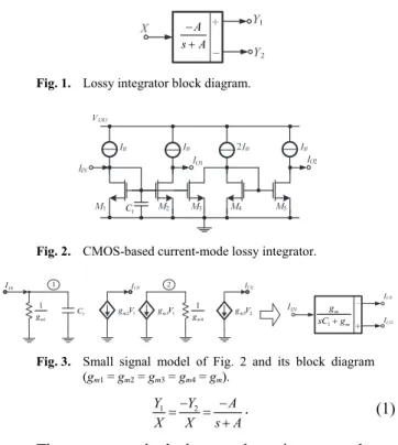
The basic lossy integrator, or first order low-pass fil-ter, used in this paper as a main building block is depicted in Fig. 1. With a single input (X) and two outputs (Y1 and
Y2) the transfer function of the lossy integrator is described
by (1)
A s A
Fig. 1. Lossy integrator block diagram.
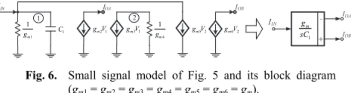
1 C
Fig. 2. CMOS-based current-mode lossy integrator.
1
m m
g sCg 1
1
m
g C1 g Vm2 1 g Vm3 1 4
1
m
g g Vm5 2
IN
I
Fig. 3. Small signal model of Fig. 2 and its block diagram (gm1 = gm2 = gm3 = gm4 = gm).
1 2
Y Y A
X X s A
. (1)
The current-mode dual output lossy integrator shown in Fig. 1 can be easily implemented on the transistor level by using MOS transistors as shown in Fig. 2. The current transfer functions can be obtained by using the small signal model shown in Fig. 3. Routine analysis of the circuit of Fig. 3 yields the current transfer functions of equations (2) and (3)
1 2
1 1
O m
IN m
I g
I sC g
, (2)
2 3 5 4 1 1
O m m m
IN m
I g g g
I sC g (3)
where gmi is transconductance of transistor i. Assume that
transistor M1 - M4 are matched (gm1 = gm2 = gm3 = gm4 = gm),
the current transfer functions of Fig. 3 become
1 1
O m
IN m
I g
I sC g
, (4)
2 1
O m
IN m
I g
I sC g . (5)
On the other hand, the lossless integrator can be easily realized by modifying the lossy integrator as follows. First, an inverting gain is added to the output of inverting lossy integrator [20]. Second, the inverted output is fed back to the input as shown in Fig. 4. Thus, the non-inverting and inverting current-mode lossless integrator transfer func-tions obtained at ports Z1 and Z2, respectively, can be
expressed as
As A
As
1 2
Z Z A
X X s
. (6)
Figure 5 shows a possible transistor level realization for the lossless integrator shown in the block diagram of Fig. 4. The output of the lossy integrator formed of tran-sistors M1, M2 and M3 is connected to the inverting gain
unit formed of transistors M4 and M5 and then fed back to
the input. There are two current outputs IOB (port Z+) and
IOA (port Z-) taken from transistors M6 and M2, respectively.
1 C
Fig. 5. CMOS-based current-mode lossless integrator.
1 m g sC 1 1 m
g C1 g Vm2 1 g Vm3 1 4
1
m
g g Vm5 2 g Vm6 2
IN
I
Fig. 6. Small signal model of Fig. 5 and its block diagram (gm1 = gm2 = gm3 = gm4 = gm5 = gm6 = gm).
Assuming that transistors M1 - M6 are matched with
gm1 = gm2 = gm3 = gm4 = gm5 = gm6 = gm, the current transfer
functions can be obtained by using the small signal model shown in Fig. 6. Routine analysis of the small signal model of Fig. 6 yields the following transfer functions
1 OA m IN I g I sC
, (7)
1
OB m
IN
I g
I sC . (8)
From Fig. 3 and Fig. 6, the input impedance of both integrators can be expressed as
1 1 in m Z g sC
. (9)
In equations (2)-(5) and (7)-(8) the transconductance gm of any transistor is given by
2
D
m OX D
GS
I
g C W L I
V
(10)
where , Cox, W and L are surface mobility, channel oxide
capacitance, channel width and channel length of the MOS transistor, respectively and ID is the bias current IB of the
transistor. Equation (10) clearly shows that transconduct-ance can be tuned by adjusting the bias current IB. Thus, the
parameters of the lossy and lossless integrators of Figs. 2 and 5 can be electronically tuned.
2.2
Synthesis of RLC Ladder Low-Pass
Filters
This section describes the synthesis procedure of lad-der filter based on the signal flow graph (SFG) method.
Two types of passive RLC ladder low-pass filter; the all-pole and Elliptic filters [21–25], are provided as prototypes. In some applications, a higher fall off rate is required in the transition band; that is a very high attenuation is required very near the cutoff frequency. This requirement mandates the use of elliptic functions in the approximation of the filter transfer function and leads to the design of Elliptic or Cauer filters [22].
Firstly, the doubly terminated current-mode third-order all-pole passive RLC ladder low-pass filter prototype shown in Fig. 7 is considered.
Fig. 7. Current-mode third-order all-pole low-pass RLC ladder prototype.
Considering the prototype shown in Fig. 7, using KCL the current and voltage relationship can be written as
1 1 IN 2
S
V
I I I
R
, (11)
1 1 1 I V sC
, (12)
2 1 3
V V V , (13)
2 2 2 V I sL
, (14)
3 3 3 I V sC
, (15)
3 3 2 L V I I R
. (16)
1 S R 1 L R 1 1 sC 3 1 sC 2 1 sL 1 L R (a) 1 m m g
sCg 3
m m
g sCg 2
m
g sC
1
I I2 I3
(b)
Fig. 8. (a) SFG of third-order all-pole low-pass ladder filter in Fig. 7, (b) Completed current-mode SFG of Fig. 8(a).
Using equations (11)-(16), a SFG can be constructed and is shown in Fig. 8(a). Voltages at different nodes and currents in different branches are forming the nodes of the SFG. The voltage nodes need to be transformed into
the voltage nodes to current nodes. The variables RS =RL
= 1/gm are used to simplify the realization method.
Further-more, lossless integrators with its negative feedback in left-hand and right-left-hand sides can be replaced by lossy inte-grators. The finalized current-mode SFG is shown in Fig. 8(b). It can be seen that the all-pole low-pass ladder filter can be designed based on lossy and lossless integra-tors.
Secondly, the passive RLC doubly terminated third-order Elliptic low-pass filter shown in Fig. 9 is also used as a prototype.
Fig. 9. Prototype current-mode third-order Elliptic low-pass RLC ladder filter.
Considering the prototype in Fig. 9, routine analysis yields the following current and voltage relationships:
1 1 IN 2 3
S
V
I I I I
R
, (17)
3 1 2 3
I V V sC , (18)
1 1 1 I V sC
, (19)
2 1
31 2
1 3 1 3
/
IN S
I I V R C
V V
s C C C C
, (20)
2
4 3 O
I I I I , (21)
4 2 4 I V sC
, (22)
2
32 1
3 4 3 4
O
I I C
V V
s C C C C
. (23)
Using (17)–(23), a modified RLC prototype can be redrawn as shown in Fig. 10. For simplicity, the current terms (IIN –I2 –V1 /RS) and (I2 – IO) in (20) and (23) are
replaced by Ix and Iy respectively and the capacitor C3 is
replaced by two new capacitors (C1 + C3) and (C3 + C4)
connected with two dependent sources as shown in Fig. 10.
3 2 1 3 C V C C
1 3
3 4 C V C C
Fig. 10. Modified current-mode third-order Elliptic low-pass RLC ladder filter.
From equations (17)–(23) and Fig. 10, a SFG can be drawn as shown in Fig. 11(a). Voltages at different nodes and currents in different branches are forming the nodes of
voltage and current in the SFG. The voltage nodes need to be transformed into current nodes. The transconductance gm is used to normalize the voltage nodes to current nodes.
The variables RS =RL = 1/gm are used to simplify the
reali-zation method. Furthermore, lossless integrators with its negative feedback in left-hand and right-hand sides can be replaced by lossy integrators. The finalized current-mode SFG is shown in Fig. 11(b). It can be seen that the elliptic low-pass ladder filter can be designed based on lossy, loss-less integrators and current gains.
3 1 3 C C C 3 3 4 C C C 1 L R 1 L R 1 S R 2 1 sL 1 3
1
s CC 3 4
1
s CC
(a) 3 1 3 C C C 3 3 4 C C C 2 m g sC
1 3
m m g
s CC g 3 4
m m g s CC g
1
I I1I2 I2
(b)
Fig. 11. (a) SFG of third-order elliptic low-pass ladder filter in Fig. 10, (b) Completed current-mode SFG of Fig. 11(a).
3.
CMOS Realization of Ladder
Low-Pass Filters
Considering the SFG shown in Fig. 8(b), the third-or-der all-pole low-pass ladthird-or-der filter can be constructed by using 2 lossy integrators and a lossless integrator. In cur-rent-mode realizations, summing and subtracting can be easily implemented by direct connection without additional circuit elements. Using the block diagrams shown in Figs. 3 and 6 and the SFG in Fig. 8(b), a third-order all-pole ladder low-pass filter can be realized as shown in the block diagram of Fig. 12.
1
m m
g
sCg 3
m m
g sCg
2
m
g sC
Fig. 12. Third-order Chebyshev low-pass ladder filter.
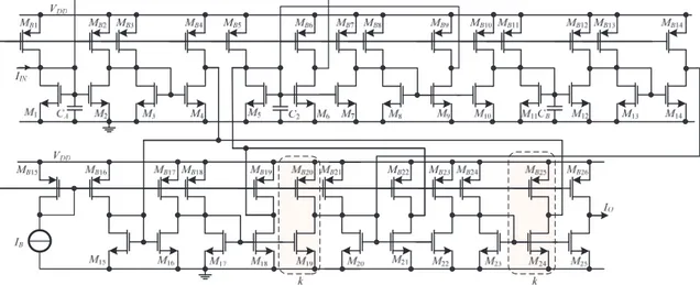
Using the block diagram in Fig. 12 and the circuits shown in Figs. 2 and 5, the complete circuit diagram of the synthesized third-order all-pole ladder low-pass filter is shown in Fig. 13. In Fig. 13, the bias currents are realized
by using PMOS current mirrors MBi with identical aspect
In a similar way using the Elliptic filter SFG shown in Fig. 11(b), the third-order Elliptic low-pass ladder filter can be constructed by using lossy, lossless integrators and additional current gains. Inspection of Fig. 11(b) shows that the SFG of Elliptic filter has two feedback paths. The cur-rent gains are needed to provide the feedback paths. Elliptic third-order ladder low-pass filter can be implemented by using the block diagrams of two lossy integrators and a lossless integrator. Two multiple outputs (+, -, k) current splitters are used to provide the current feedback between I’1 and I’2. It can be seen that the proposed circuit requires
only three capacitors while the prototype RLC filter uses three capacitors and one inductor. The current-gain can be easily realized by defining the aspect ratios of the particular transistors and its bias current. Using the SFG in Fig. 11(b), the design of third-order elliptic low-pass ladder filter can be realized by using the block diagram of two lossy inte-grators, one lossless integrator and two current splitters as shown in Fig. 14.
Using the block diagram in Fig. 14 and the circuits shown in Figs. 2 and 5, the complete circuit of the third-order Elliptic low-pass ladder filter is shown in Fig. 15. It can be seen that the proposed circuit requires only three capacitors while the prototype RLC filter of Fig. 9 requires three capacitors and one inductor. In Fig. 15 the bias
currents are implemented using PMOS current mirrors MBi
with identical aspect ratios for providing the equal bias currents. As shown in the block diagram in Fig. 14, two extra current amplifiers with current gain k are required. In Fig. 15 these current amplifiers are realized by using the MOSFET transistors shown in the two dotted boxes. Note that the capacitors used in the circuits are on-chip type [26] as shown in Fig. 16. These capacitors can be simultane-ously implemented with the whole circuit on the chip for full integration. This would also enable high frequency operation as it reduces the parasitic capacitances associated with of-the-chip connections.
2
C
1
C C3
Fig. 13. CMOS current-mode tunable 3rd order all-pole low-pass ladder filter.
1 3
m m
g s CC g
2
m
g
sC 3 4
m m
g s CC g
3 34
C k
C C
1 3 3
C k
C C
Fig. 14. Third-order Elliptic low-pass ladder filter.
4.
Effect of Non-idealities
This section shows the influence of the NMOS tran-sistors parasitic elements. Lossy and lossless integrators are the main building blocks of the proposed filters. Therefore, due to the transistor parasitic elements, when the circuits work at relatively high-frequencies their performances may deviate from the theory. Non-ideal analysis of integrators can be performed by using the small signal model of NMOS in Fig. 16.
ox ox
C C W L
Fig. 16. NMOS capacitor used for the grounded capacitors.
m gs
g v
Fig. 17. Small signal model of MOS transistor.
In the small signal model shown in Fig. 17, the input parasitic capacitances Cgsand Cgd, the conductance gds and
the transconductance gm are incorporated. The effects of the
transistor parasitic components on the performance of the proposed low-pass filters are described in the following subsections.
4.1
Parasitic Capacitances
This section will consider the effect of the parasitic capacitances Cgd and Cgs, which is important for
determin-ing the performance of a CMOS circuit, particularly at high frequencies.
4.1.1 Lossy Integrators
Using the small signal model of MOS transistor of Fig. 17, considering only the parasitic gate-drain capaci-tance Cgd, that affects the inverting and non-inverting lossy
integrator, and assuming that the transconductances of MOS transistors are matched, then transfer functions of the lossy integrator of Fig. 2 can be approximated by (24) and (25), respectively
1
2 1
( )
O m
IN m gd
I g
I g s C C
, (24)
2
2 4 1
3
O m
IN m gd gd
I g
I g s C C C
. (25)
Similarly, considering the parasitic gate-source
capacitance Cgs that affects inverting and non-inverting
lossy integrator, and assuming that the transconductances of MOS transistors are matched, then the transfer functions of the lossy integrators are given by (26) and (27), respectively
1
1 2 1
( )
O m
IN m gs gs
I g
I g s C C C
, (26)
2
3 4 1 2 1
O m
IN m gs gs gs gs
I g
I g s C C C C C
. (27)
Equations (23)-(26) show the effect of the parasitic capacitances on the performance of the lossy integrator. In saturation operation, the parasitic gate to drain capacitance Cgd and gate to source capacitance Cgs will vary anywhere
within the ranges depending on the bias conditions in-volved [22]. For the specific case where it is assumed that the parasitic capacitances Cgdi = Cgd, Cgsi = Cgs with Cgd =
WLDCox and Cgs = W((2/3)(L)+LD))Cox, it can be seen that
parasitic capacitances Cgd and Cgs produce a small
devia-tion in the frequency response of the low-pass filter. To prevent significant errors, the capacitance C1 should be
1 4 gs gd
C C C . (28)
4.1.2 Lossless Integrators
In a similar way, the effect of the parasitic gate-drain and gate-source capacitances Cgd and Cgs, that affect the
inverting and non-inverting lossless integrator of Fig. 5 can be considered. Assuming that the transconductances of MOS transistors are matched, the transfer functions of the lossless integrators affected by the parasitic capacitances Cgd and Cgs can be expressed as
4 3 4 5 2 1
OA m
IN gd gd gd
I g
I s C C C C
, (29)
4 2 4 4 5 1
OB m
IN gd gd gd
I g
I s C C C C
, (30)
1 2 3 4 5 1
OA m
IN gs gs gs gs gs
I g
I s C C C C C C
, (31)
1 2 3 4 5 1
OB m
IN gs gs gs gs gs
I g
I s C C C C C C
. (32)
Inspection of equations (29)-(32), shows the effect of the parasitic capacitances Cgd and Cgs on the performance
of the lossless integrator. In saturation region, the parasitic gate to drain and source capacitances Cgd and Cgs will vary
anywhere within the ranges depending on the bias condi-tions involved. To prevent significant errors, the selected capacitance C1 should be
1 9 gd 5 gs
C C C . (33)
From (33), it is clear that the errors can be minimized by selecting relatively large values for the capacitance C1.
4.2
Parasitic Resistance
r
dsThe most commonly used small-signal model for a MOS transistor operating in the active region is shown in Fig. 17. The voltage-controlled current source gmvgs is the
2
1 2
n ox
DS GS T DS
C W
i v V v
L
(34)
where represents the channel-length modulation effect
which is normally less than 1. It produces the slope of drain current as a function of the voltage vDS. The channel
con-ductance will be dependent upon L through which is
inversely proportional to L (1/L). The small-signal channel conductance gds is expressed as
1
1
DS DS
ds DS
ds DS DS
i i
g i
r v v
. (35)
Equation (35) shows the direct effect of the drain cur-rent (bias curcur-rent) and the channel-length modulation on gds .This would affect the gain and the cut-off frequency of
the filter. It is a trade-off situation especially if short-chan-nel (L < 5 µm) is used in order to minimize the die area of the chip and its power consumption. However, the resulting small reduction in gain of the filters may be tolerated and can be easily compensated in the succeeding stages.
4.2.1 Lossy Integrators
Using the small signal model of MOS transistor with parasitic conductance and assuming that the transconduct-ances of the MOS transistors are matched, where it is as-sumed that gmi = gm and gdsi = gds the transfer functions of
the lossy integrators can be approximated by
1 1
1
( 2 ) ( )
2 ( 2 ) ( )
O m ds m m ds m ds
IN m ds m m ds m ds
I g g g g g C g g
I g g s g g g C g g
, (36)
2 1
1
( 3 ) ( 2 )
3 ( 3 ) ( 2 )
O m m m ds m ds
IN ds m m m ds m ds
I g g g g C g g
I g g s g g g C g g
. (37)
Inspection of equation (36) and (37) clearly shows that magnitude and the cut-off frequency of the lossy inte-grators will be slightly affected by gds. In order to avoid
significant errors in the transfer functions of the lossy inte-grators the transistor transconductance gm must satisfy the
condition
3
m ds
g g . (38)
Inspection of equations (10) and (38) shows that sig-nificant errors can be avoided if large transistor width W is used.
4.2.2 Lossless Integrators
In a similar way, taking into consideration the effect of the parasitic drain-source conductance gds, the transfer
functions of the inverting and non-inverting lossless inte-grators can be expressed as
2
1 3 4 5 1 3 4
m OA
IN m ds ds ds ds m ds ds
g I
I g g g g g sC g g g
, (39)
2
1 2 3 4 1 2 3
m OB
IN m ds ds ds ds m ds ds
g I
I g g g g g sC g g g . (40)
Equations (39) and (40) show how the parasitic drain to source conductance gds affects the transfer functions of
the lossless integrator. Assuming that the transconduct-ances of MOS transistors are matched equations (39) and (40) reduce to
1
1 1
4
4 4 4
OA m m ds
IN ds ds ds
I g g g C
I g sC g s g C
, (41)
1
1 1
4
4 4 4
OB m m ds
IN ds ds ds
I g g g C
I g sC g s g C
. (42)
From equations (41) and (42), it can be seen that both types of lossless integrator are affected by the parasitic
conductance gds as a parasitic pole at low frequency
ωL = 4gds / C1 will appear in each transfer function.
How-ever, these effects will be significant at very low-frequency where the working frequency is much less than the fre-quency of the parasitic pole. Thus, the resulting parasitic poles will provide the lower frequency limitation of loss-less integrators and the maximum gain at low frequency
k= gm /4gds.
4.3
Transistor Mismatches
This section will consider the effect of transistor mismatches on the performance of the proposed integrator circuits.
4.3.1 Lossy Integrators
Consider the lossy integrator circuit of Fig. 2. Using the small signal model of the MOS transistor of Fig. 17, ignoring the effects of Cgs andgds and assuming that the
transconductances of the MOS transistors are gm1 and gm2
for the transistors M1 and M2 respectively, reanalysis shows
that the transfer function of the lossy integrator of Fig. 2 can be expressed by (43)
1 2 2 1
1 1 1
O O m m
IN IN m m
I I g g
I I g g sC
. (43)
Inspection of equation (43) shows that, due to the transistor mismatch, the low frequency gain of the lossy integrator will deviate from unity as predicted by equations (4) and (5). This effect is not significant and can be easily compensated, if required, by an additional current amplifier or attenuator.
4.3.2 Lossless Integrators
In a similar way the effect of transistors mismatch on the performance of the lossless integrator of Fig. 5 can be studied. Using the small signal model of the MOS transis-tor of Fig. 17, ignoring the effects of Cgs andgds and
as-suming that the transconductances of the MOS transistors are gm1 for the transistor M1 and gm2 for the transistors M2
and M3 respectively, reanalysis shows that the transfer
1 2 1
2 sC g g
g I
I I I
m m
m
IN OB
IN OA
.
(44)Inspection of equation (44) shows that, due to the transistor mismatch, the lossless integrator becomes a lossy integrator with a very low frequency pole at
1 2 1
C g
gm m
p
. (45)
This low-frequency pole will be at zero frequency when gm1 = gm2 resulting in an ideal lossless integrator. But
it may be moved slightly in the right-half plane if gm1 > gm2
or slightly in the left-half plane if gm1 < gm2. Thus, in order
to avoid any unexpected performance care must be taken to ensure that gm1 gm2. This can be easily achieved by
trim-ming the bias currents of the transistors.
5.
Simulation Results
This section describes the simulation results of the proposed electronically tunable current-mode ladder third-order low-pass filters. PSPICE simulation results are car-ried out by using TSMC 0.18 µm CMOS technology, +1.5 V power supply. The extracted small signal
parame-ters of NMOS and PMOS are n = 0.1 V-1, nCox =
100 A/V2, VTHn = 0.37 V and p = 0.1 V-1, pCox =
25 A/V2, VTHp = 0.38 V respectively. The minimization of
the aspect ratio W/L is required for obtaining the desired
transconductance with minimum error and die area. Thus, the aspect ratios of the transistors used in Figs. 13 and 15 were selected as W/L= 70 µm/0.36 µm. The bias currents
IB are provided by using positive current mirrors (PMOS)
with identical aspect ratio W/L = 100 µm / 0.36 µm. The
special NMOS transistors (M19 and M24) of Fig. 15 use
W/L = 4.8 µm / 0.36 µm for obtaining the current gain
k = 0.07. The special PMOS transistors (MB20 and MB25) of
Fig. 15 use of W/L = 6.8 µm / 0.36 µm to achieve the bias current 0.07IB.
The simulated DC transfer characteristic of the pro-posed lossy integrator is shown in Fig. 18. Inspection of Fig. 18 clearly shows that large values of channel length L result in smaller error and DC-offset than the small values
of L. However, it is a trade-off between the error and die
area minimizations. Using more accurate current mirror structures; for example cascode current mirrors and large
values of L would result in smaller errors but a large die
area, complex structures and more power consumption will be the price for this reduced error.
In order to verify the operation of the transistors in the saturation region, the values of VGSand VDS were monitored
over the bias current range [0.03, 0.3, 3, 30, 300] µA for the transistors M1 and M2 of the lossy integrator of Fig. 2
and transistors M1-M5 of the lossless integrator of Fig. 5. In
all cases it was found that VDS > VGS – VTHN and VGS > VTHN.
Thus, the operation of the transistors in the saturation region is confirmed for the bias current range of interest.
Fig. 18. DC-characteristic of the proposed lossy integrator using different values of W/L.
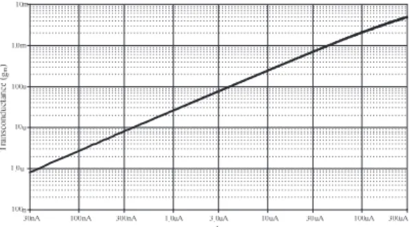
Fig. 19. Transconductance of a MOS transistor against its bias current.
Variations of the transconductance of the MOS transistor were also measured as a function of the bias current of the transistor aspect ratio W/L= 70 µm / 0.36 µm. The result shown in Fig. 19 confirms the dependence of the transcon-ductance on the bias current.
The frequency response of CMOS lossy integrator of Fig. 2 and CMOS lossless integrator of Fig. 5 are depicted in Fig. 20 and 21, respectively. As explained in Sec. 4.1,
the capacitor C1 = 10 pF is selected for minimizing the
effect of parasitic capacitances and the bias current IB was
varied in the range [0.03, 0.3, 3, 30, 300] µA. Figures 20 and 21 clearly show that the frequency response can be tuned, using the bias current, over a wide range of frequen-cies (10 kHz to 100 MHz). From Fig. 21, the low-fre-quency current gain of the lossless integrator is around 25 dB. This agrees well with the theory presented in Sec. 4.2.2. Inspection of Fig. 21 clearly shows that there is a parasitic zero in the gain-frequency characteristic. This parasitic zero can be attributed to the parasitic output re-sistances of the MOSFETs which is inversely proportional to the transistor length L. Thus, for L = 0.36 µm and bias current IB = 300 µA the output resistance of the transistor
Fig. 20. Magnitude and phase responses of CMOS lossy integrator of Fig. 2 by varying bias current IB.
Fig. 21. Magnitude and phase responses of CMOS lossless integrator in Fig. 5 by varying bias current IB.
Fig. 22. Comparison of proposed all-pole LPF with RLC prototype (IB = 2.7 μA).
The specifications of the prototype third-order filter with Chebyshev response are as follows: Cut-off frequency = 2 MHz, Amax = –6 dB and passband ripple = 0.1 dB [27].
The RLC prototype of Fig. 7 was simulated using the fol-lowing components, C1 = C3 = 128 nF, L2 = 88 nH, RS = RL
= 1 Ω and the proposed all-pole filter of Fig. 13 was simu-lated using the following components, the capacitors C1 =
C3 = 12 pF (W/L = 40 µm / 40 µm), C2 = 8 pF (W/L =
32 µm / 32 µm) and bias current IB = 2.7 μA. The simula-
Ga
in
(d
B)
Fig. 23. Magnitude response of proposed third-order all-pole LPF as a function of the bias current IB.
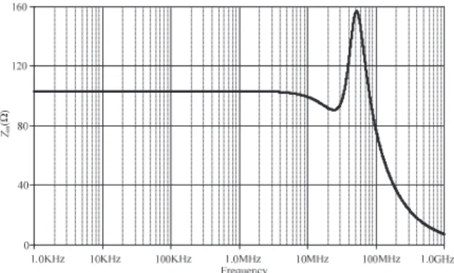
Fig. 24. Input impedance of the proposed all-pole low-pass filter at bias current IB = 300 µA.
Fig. 25. Group delay of the proposed all-pole low-pass filter at bias current IB = 300 µA.
tion results obtained from the RLC prototype filter of Fig. 7 and the proposed all-pole filter in Fig. 13 is shown in Fig. 22. It can be seen that the frequency response of the proposed filter and the RLC prototype are very close but the slope of the stop band has slight deviations. The elec-tronically-tuned feature of the proposed third-order all-pole low-pass filter can be provided by adjusting the bias cur-rent IB [0.03, 0.3, 3, 30, 300]µA. The frequency response
of the filter can be tuned over a wide range of frequencies (10 kHz and 100 MHz) as shown in Fig. 23. It can be seen that the results are in agreement with the theoretical pre-dictions.
Figure 24 shows that the variation of the input
imped-ance at a bias current IB = 300 µA. Inspection of Fig. 24
shows that the input impedance is around 100 Ω along the
almost zero within the stop-band. Thus, the input imped-ance is relatively low over a wide range of the pass band. Figure 25 shows the group delay of the proposed all-pole low-pass filter. It can be seen that the group delay is flat along the pass-band with a value around 4 ns.
The specifications of the prototype third-order Elliptic filter are as follows: the cut-off frequency = 2MHz, Amax =
–6 dB, Amin = –35 dB, and passband ripple = 0.1 dB [27].
The Elliptic prototype low-pass filter of Fig. 9 was
simulated using the following components: C1 = C4 =
120 nF, C3 = 11.4 nF, L2 = 102.8 nHandRS = RL = 1 Ω. The
proposed Elliptic filter of Fig. 15 was simulated using the following components: CA = CB = (C1 + C3) = (C3 + C4)
= 8.5 pF (W/L = 50 µm / 50 µm) and C2 = 7.5 pF (W/L
= 45 µm / 45 µm) and bias current IB = 5 µA. The
simulation results obtained from the proposed Elliptic LPF and the RLC prototype are depicted in Fig. 26. It can be seen that the magnitude response of the proposed Elliptic filter is quite similar to that of the prototype Elliptic filter but the stop-band magnitude is slightly different.
The electronically-tuned feature of the proposed third-order Elliptic low-pass filter can be provided by adjusting the bias current IB [0.03, 0.3, 3, 30, 300] µA. The frequency
response of the filter can be tuned over a wide frequency range as shown in Fig. 27. It can be seen that the results are in good agreement with the theoretical predictions.
Figure 28 shows the variation of the input impedance of the Elliptic low-pass filter. The input impedance with bias current IB = 300 µA is obtained around 100 Ω along
Fig. 26. Comparison of the proposed Elliptic LPF with the RLC prototype.
Fig. 27. Magnitude response of the proposed third-order Elliptic LPF as a function of the bias current IB.
Fig. 28. Input impedance of the proposed Elliptic low-pass filter at bias current IB = 300 µA.
Fig. 29. Group delay of the proposed Elliptic low-pass filter at bias current IB =300 µA.
the pass-band frequency of around 100 MHz and becomes almost zero in the stop-band. Thus, the input impedance is relatively low over a wide range of the pass band. Fig. 29 shows the group delay of the proposed Elliptic low-pass filter at bias current IB = 300 µA. It can be seen that the
group delay is flat along the pass-band with a value around 4 ns.
The performance of the proposed third-order all-pole and Elliptic low-pass filters can also be verified by apply-ing multi tones (10, 40, 70, 100, 130, 160, 190 and 220 MHz) to the filters at the bias current equal to 300 µA. From Figs. 30 and 31, it appears that the out-of-band tones (> 100 MHz) have been removed and only the in-band tones (< 100 MHz) can be obtained at the output. Further-more, it can be seen that, with the same order of the filter, the characteristic of the Elliptic filter is better than that of the all-pole counterpart especially in removing signals in the stop-band.
The total harmonic distortion (THD) of the proposed third-order all-pole and Elliptic low-pass filters was meas-ured and the results are shown in Fig. 32 and 33, respec-tively. The results were obtained by applying two sinusoids with variable amplitudes at two frequencies (1 MHz and
10 MHz) with bias current IB = 300 µA. The THD at
10 MHz of the proposed filters are found to be below 0.7% and 0.6%, respectively.
Fig. 30. Multi tones measurement of the proposed third-order all-pole low-pass filter at bias current IB = 300 µA.
Fig. 31. Multi tones measurement of the proposed third-order Elliptic low-pass filter at bias current IB = 300 µA.
Fig. 32. THD of the proposed third-order all-pole low-pass filter at bias current IB = 300 µA.
Fig. 33. THD of the proposed third-order Elliptic low-pass filter at bias current IB = 300 µA.
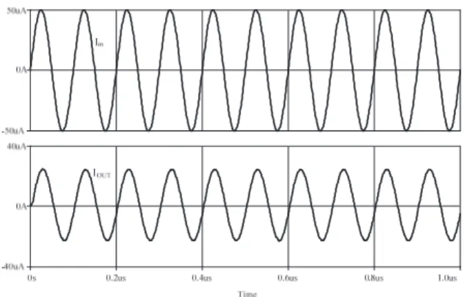
Fig. 34. Input and output of 10 MHz waveforms of Chebyshev LPF at bias current IB = 300 µA.
Fig. 35. Input and output of 10 MHz waveforms of the Elliptic LPF at bias current IB = 300 µA.
10 MHz with 30 µAp-p are applied to the both filters. It can
be seen that the sinusoidal signal can be obtained at the outputs of the proposed Chebyshev and Elliptic filters as shown in Fig. 34 and 35, respectively. It is evidently found that in-band signal can be passed the proposed filters with low distortion.
Transistor mismatches are the major sources of errors in the proposed MOSFET based filters. To investigate the effect of transistor mismatches on the performance of the proposed filters Monte Carlo analysis was performed. A hundred of samples are run for verifying the frequency response. The 2% uniform deviation of NMOS transistors surface mobility with bias current IB = 300 µA is
as-sumed. The results are shown in Figs. 36 and 37. Inspec-tion of Fig. 36 shows that the cutoff frequency of the filter deviates from its nominal value by about ±2 MHz which corresponds to ±2%.
Inspection of Fig. 37 shows that the cut-off frequency of the Elliptic filter deviates from its nominal value by about ±2 MHz which corresponds to ±2% error. In order to investigate the feasibility of integrated circuit fabrication and to estimate the area on the chip of the proposed cir-cuits, the physical layout of the proposed low-pass Cheby-shev and Elliptic filters were obtained and are shown in Figs. 38 and 39 respectively. The resulting dimensions of
these layouts are approximately 200 µm 240 µm and
210 µm 360 µm, for Chebyshev and Elliptic filters,
LP Cut-off frequency (Hz)
94M 101M
0 5 10 15 20 P e r c e n t o f S a m p l e s
n samples = 100 n divisions = 10 mean = 9.74368e+007
sigma = 862276 minimum = 9.56369 e+007 10th %ile = 9.6256e+007
median = 9.74336e+007 90th %ile = 9.84359e+007 maximum = 9.94538e+007
Fig. 36. Monte Carlo analysis of the cut-off frequency of the all-pole low-pass filter based on 2% surface mobility deviations the of NMOS transistors (M1-M15) with IB =
300 µA.
LP Cut-off frequency (Hz)
108M 118M
0 10 20 30 P e r c e n t o f S a m p l e s
n samples = 100 n divisions = 10 mean = 1.13106e+008
sigma = 1.23734e+006 minimum = 1.09721e+008 10th %ile = 1.11579e+008
median = 1.13253e+008 90th %ile = 1.14784e+008 maximum = 1.1595e+008
Fig. 37. Monte Carlo analysis of the cut-off frequency of the Elliptic low-pass filter based on 2% surface mobility deviations of the NMOS transistors (M1-M25) with IB =
300 µA.
Fig. 38. The physical layout of the low-pass Chebyshev filter.
Table 1 shows a comparison of the performance of the proposed all-pole and Elliptic third-order ladder low-pass filters with previously published filters. Most of the previ-ous works cannot be operated at relatively very high fre-quencies and have no electronic tunability feature because of the limitation of the used active devices. Most of the pervious works use excessive number of transistors and relatively large power supply voltages. It can be seen that the proposed filters use a low number of components without any externally connected resistors compared with previously published works. Table 1 shows that electronic
Fig. 39. The physical layout of the Elliptic low-pass filter.
Filters Power supply
Frequency range
Number of transistors
Use of resistors
Electronic Tunability
Power Dissipation (IB=100µA)
THD
[7] +1.5 V >10 MHz 146 No Yes 6.2 mW <1% [8] ±2 V <100 MHz 154 No Yes NA NA [9] ±5 V <10 MHz 104 No No 14 mW <1% [10] ±5 V <100 MHz 72 No No NA NA [11] ±3 V <10 MHz 123 No No NA NA [12] ±1 V <10 MHz 123 No No NA NA [13] ±1 V <10 MHz 85 Yes No NA NA [14] ±2.5 V <10 MHz 90 Yes No NA NA [15] ±1.8 V <10 MHz 171 No No NA NA [16] ±2.5 V <10 MHz 84 Yes No NA NA Proposed1 +1.5 V <100 MHz 31 No Yes 3 mW <1% Proposed2 +1.5 V <100 MHz 53 No Yes 5 mW <1%
Tab. 1. Comparison of previous works with the proposed filters.
tunability, low power dissipation (at same bias current) and operation at relatively very high frequencies are the most outstanding features of the proposed filters.
6.
Conclusion
CMOS third-order current-mode all-pole and Elliptic low-pass filters based on RLC ladder prototype have been proposed. The filters are built around lossy and lossless integrators, current splitters and grounded capacitors. They enjoy wide tuning range of the frequency responses in the range 10 kHz and 100 MHz by using bias current from 0.03 µA to 300 µA. The circuits use only single +1.5 V DC power supply with dynamic power consumption around 8.9 mW and 16.9 mW (300 µA bias current) and occupied
200 µm 240 µm and 210 µm 360 µm, for Chebyshev
and Elliptic filters, respectively. The proposed circuits enjoy low complexity structures, with low number of components, low-voltage, low THD, relatively low input impedance and high-frequency operation. All the proposed filters are suitable for integration and can be used for high frequencies up to the VHF range.
References
[1] RAUT, R., SWAMY, M. N. S. Modern Analog Filter Analysis and Design. Weinheim (Germany): Wiley-VCH Verlag GmbH & Co. KGaA, 2010. ISBN: 9783527407668
Circuits and Systems MWSCAS. Aug. 1997, vol. 1, p. 241–244. DOI: 10.1109/MWSCAS.1997.666078
[3] FABRE, A., DAYOUB, F., DURUISSEAU, L., KAMOUN, M. High input impedance insensitive second-order filters implemented from current conveyors. IEEE Transactions on Circuits and Systems I: Fundamental Theory and Applications, Dec. 1994, vol. 41, no.12, p. 918–921. DOI: 10.1109/81.340859
[4] LUCK, J., SWANSON, J. G. First-order, switched-capacitor, low-pass filter implemented with GaAs insulated-gate FET switches. Electronics Letters, Oct. 1990, vol. 26, no. 22, p. 1843–1845. DOI:10.1049/el:19901186
[5] BANERJEE, K., RANJAN, A., PAUL, S. K. New first order multifunction filter employing operational transresistance amplifier. In Proceedings of 5th International Conference on Computers and Devices for Communication (CODEC 2012). Dec. 2012, p. 1–3. DOI: 10.1109/CODEC.2012.6509218
[6] CHEN, W. K. The Circuits and Filters Handbook. A CRC Handbook Published in Cooperation with IEEE Press, 1995. ISBN: 9781420055276
[7] SA-AD, S., CHAYTHONG, D. A high frequency current-mode ladder filter using multiple output lossless integrator. In Proceed-ings of International Symposium on Intelligent Signal Processing and Communications Systems, ISPACS 2008. Feb. 2009, p. 1–4. DOI:10.1109/ISPACS.2009.4806743
[8] JIRASEREE-AMORNKUN, A., FUJII, N., SURAKAMPON-TORN, W., Realization of electronically tunable ladder filters using multi-output current controlled conveyors. In Proceedings of the International Symposium on Circuits and Systems 2003, ISCAS’03. May 2003, vol. 1, p. 541–544. DOI:10.1109/ ISCAS.2003.1205620
[9] ZELE, R. H., ALLSTOT, D. J., FIEZ, T. S. Fully balanced CMOS current-mode circuits. IEEE Journal of Solid-State Circuits, 1993, vol. 28, no. 5, p. 569–575. DOI: 10.1109/4.229398
[10] ORALKAN, O., KARSILAYAN, A. I., TAN, M. A. Design of all-pole low-pass ladder filters using current-mode damped integrators. In Proceedings of the International Symposium on Circuits and Systems, ISCAS’96. May 1996, vol. 1, p. 266–269. DOI: 10.1109/ISCAS.1996.539880
[11] WU, J., EL-MASRY, E. A new approach of design of current-mode filters. In Proceedings of International Symposium on Circuits and Systems, ISCAS’97. Jun. 1997, vol. 1, p. 317–320. DOI: 10.1109/ISCAS.1997.608721
[12] WU, J., EL-MASRY, E. Design of current-mode ladder filters using coupled-biquads. IEEE Transactions on Circuits and Systems II: Analog and Digital Signal Processing, Nov. 1998, vol. 45, no. 11, p. 1445–1454. DOI: 10.1109/82.735356
[13] TANGSRIRAT, W., FUJII, N., SURAKAMPONTORN W. Current-mode leapfrog ladder filters using CDBAs. In Proceedings of International Symposium on Circuits and Systems, ISCAS 2002. 2002, vol. 5, p. 57–60. DOI: 10.1109/ISCAS. 2002.1010639
[14] YAN-HUI, X., XUE, L. Active simulation of passive leapfrog ladder filters using DVCCs. In Proceedings of International Con-ference on Industrial Technology, ICIT 2008. Apr. 2008, p. 1–5. DOI:10.1109/ICIT.2008.4608606
[15] YAN-HUI, X., PENG, H. Realization of low-pass and band-pass leapfrog filters using OAs and CCCIIs. In Proceedings of International Conference Management and Service Science, MASS’09. Sep. 2009, p. 1–4. DOI: 10.1109/ICMSS.2009.5303743
[16] WU, J., EL-MASRY, E. Current-mode ladder filters using multiple output current conveyors. IEE Circuits, Devices and Systems, 1996, vol. 143, no. 4, p. 218–222. DOI: 10.1049/ip-cds:19960490
[17] YUCE, E., MINAEI, S. On the realization of high-order current-mode filter employing current controlled conveyors. Computers
and Electrical Engineering, May 2008, vol. 34, no. 3, p. 165–172. DOI:10.1016/j.compeleceng.2007.04.001
[18] YUCE, E., MINAEI, S. ICCII-based universal current-mode analog filter employing only grounded passive components. Analog Integrated Circuits and Signal Processing, Feb. 2009, vol. 58, no. 2, p. 161–169. DOI: 10.1007/s10470-008-9225-2
[19] SINHA, P. K., SAINI, A., KUMAR, P., MISHRA, S., CFOA based low pass and high pass ladder filter—a new configuration. Circuits and Systems, 2014, vol. 5, no. 12, p. 293–300. DOI: 10.4236/cs.2014.512030
[20] PROMMEE, P., WONGPROMMOON, N. Tunable CMOS-based current mode fifth-order ladder low-pass filter. In Proceedings of the 36th International Conference on Telecommunications and Signal Processing (TSP). Jul. 2013, p. 397–401. DOI: 10.1109 /TSP.2013.6613961
[21] ANANDA MOHAN, P. V. Current-Mode VLSI Analog Filters: Design and Applications. Birkhauser Boston, 2003. ISBN: 9781461200338
[22] DELIYANNIS, T., SUN, Y., FIDLER, J. K. Continuous-Time Active Filter Design. London (UK): CRC Press, 1999. ISBN: 9780849325731
[23] SCHAUMANN, R., GHAUSI, M. S., LAKER, K. R. Design of Analog Filters: Passive, Active RC and Switched Capacitor. Prentice Hall, 1995. ISBN: 9780132002882
[24] ALLSTOT, D. J., BRODERSEN, R. W., GRAY, P. R. Fully-integrated high-order NMOS sampled-data ladder filters. In Proceedings ofIEEE Intl. Solid-State Circuits Conf. New York, 1978, vol. 21, p. 82–83. DOI. 10.1109/ISSCC.1978.1155789
[25] PENNEY, W. M., LAU, L. MOS Integrated Circuits, Theory, Fabrication, Design, and Systems Applications of MOS LSI. American Micro-Systems Inc., 1972. ISBN: 9780442203528
[26] BAKER, R. J. CMOS Circuit Design, Layout, and Simulation. Wiley - Interscience. 2008. ISBN: 9780470881323
[27] HUELSMAN, L. P. Active and Passive Analog Filter Design. McGraw-Hill Inc., International Edition, 1993. ISBN: 9780070308602
About the Authors...
Terdsak KUNTO received B. Ind. Tech. degree in
Tele-communications from the Faculty of Engineering, King Mongkut’s University of Technology North Bangkok (KMUTNB), Bangkok, Thailand in 2009, and M.Eng. degree in Telecommunications Engineering from the Fac-ulty of Engineering, King Mongkut’s Inst. of Technology Ladkrabang (KMITL), Bangkok, Thailand in 2013. He is now pursuing a doctoral degree in Electrical Engineering, KMITL.
Pipat PROMMEE received his B. Ind. Tech. degree in
analog filter design and CMOS analog integrated circuit design. He is a member of IEEE, USA.
Muhammad Taher ABUELMA’ATTI was born in Cairo,
Egypt, in 1942. He received the B.Sc. degree in Electrical Engineering from the University of Cairo, Cairo, Egypt, in 1963, and the Ph.D. degree and the Doctor of Science de-gree, both from the University of Bradford, Bradford, England, in 1979 and 1999, respectively. From 1963 to 1967, he was at the Military Technical College, Cairo, as a Teaching Assistant. He was with the Iron and Steel Com-pany in Helwan, Cairo, from 1967 to 1973 as a Senior Electrical Engineer. From 1973 to 1976, he was with the College of Engineering, University of Riyadh, Riyadh, Saudi Arabia, as a Teaching Assistant. From 1980 to 1981, he was with the Faculty of Engineering, University of Khartoum, Khartoum, Sudan, as an Assistant Professor, and from 1981 to 1982 he was with the College of