Advances in Radio Science, 3, 355–358, 2005 SRef-ID: 1684-9973/ars/2005-3-355
© Copernicus GmbH 2005
Advances in
Radio Science
A new circuit technique for reduced leakage current in Deep
Submicron CMOS technologies
A. Schmitz1,*and R. Tielert1
1Technische Universit¨at, Kaiserslautern, Germany *now at: Continental Teves, Frankfurt a. M., Germany
Abstract. Modern CMOS processes in the Deep Submicron regime are restricted to supply voltages below 2 volts and further to account for the transistors’ field strength limita-tions and to reduce the power per logic gate. To maintain the high switching performance, the threshold voltage must be scaled according with the supply voltage. However, this leads to an increased subthreshold current of the transistors in standby mode (VGS=0). Another source of leakage is gate current, which becomes significant for gate oxides of 3nm and below.
We propose a Self-Biasing Virtual Rails (SBVR) – CMOS technique which acts like an adaptive local supply voltage in case of standby mode. Most important sources of leakage currents are reduced by this technique. Moreover, SBVR-CMOS is capable of conserving stored information in sleep mode, which is vital for memory circuits.
Memories are exposed to radiation causing soft errors. This well-known problem becomes even worse in standby mode of typical SRAMs, that have low driving performance to withstand alpha particle hits. In this paper, a 16-transistor SRAM cell is proposed, which combines the advantage of extremely low leakage currents with a very high soft error stability.
1 Introduction
Low leakage currents in standby mode are crucial for battery-driven devices with increasing complexity. The discharge time of a battery is basically given by the power consump-tion in sleep mode, rather than in actice mode. Since also memories are integrated on a chip, there is the need for a new circuit topology which helps to reduce standby currents, and prevents losses of information.
Correspondence to: A. Schmitz
2 Leakage current components
The main sources of leakage currents are subthreshold cur-rent, DIBL, GIDL, and gate leakage. Drain-Induced Barrier Lowering is known as the DIBL effect. High voltages be-tween drain and source reduce the charge being controlled by the gate, thus having the same effect as lowering the thresh-old voltage (Tsividis, 1987).
Gate-Induced Drain Leakage (GIDL) is mainly based on band-band tunneling between the overlap region of gate and drain because of deep depletion in this area (Chan, 1987).
Gate leakage current is a tunneling effect between gate and drain, or source, respectively. This leakage current plays a decisive role in deep submicron technologies with very thin gate oxide thicknesses (v. Ardenne et al., 1997).
Due to the limited subthreshold current slope, MOS tran-sistors are prone to high subthreshold currents if threshold voltages become too low. Clever combination of low-vt tran-sistors for high switching speed and high-vt trantran-sistors for re-duced leakage current can be a good compromise for circuit designs, in order to reach an acceptable overall performance.
3 Rules for the dimensioning of MTCMOS circuits
The MTMCOS technique (Mutoh et al., 1995) is a well-known way to combine high switching speed with low standby current, by using low-vt transistors for the logic part and high-vt transistors for the so-called sleep transis-tors. However, a practical analytic formula, how to correctly dimension the sleep transistor for a demanded performance, has not been provided.
356 A. Schmitz and R. Tielert: Reduced leakage current in Deep Submicron CMOS technologies
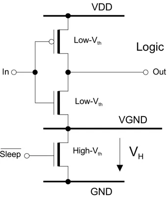
VDD
In
Out
GND
VGND
Sleep
Low-V
thLow-V
thHigh-V
thLogic
V
HFig. 1. Modified MTCMOS design with NMOS sleep control
tran-sistor.
following equation describes the resulting ”ground shift”VH due to the sleep transistor.
VH =
q−1
q ·(V0−Vt hL) . (1)
The factorq (q>1) is used to describe the specified de-lay time factor of the MTCMOS circuit in comparison to a standard CMOS configuration.
With the help of Eq. (1) it is possible to calculate the neces-sary widthWHof a sleep transistor, withWLas the accumu-lated width of all low-Vt logic transistors that are controlled by the sleep transistor.
WH =0.625·
WL 2 ·
V0−Vt hL−VH
(V0−Vt hL)·VH −
V2
H 2
. (2)
A drawback of the common MTCMOS technique is the floating of nodes in the circuits. To prevent data from being lost, circuitry must be added to each flipflop.
By use of Eq. (2) the logic part of a 256kBit-SRAM has been redesigned from standard CMOS to MTCMOS. Mea-sured read access times are negligibly longer compared to CMOS (<5%), but leakage current can be reduced by a fac-tor of 30. Figure 2 shows a picture of the fabricated SRAM chip.
Since SRAM cells cannot be realized in MTCMOS due to the loss of information in standby mode this technique is limited to normal logic applications. Besides, other leakage currents than subthreshold current are not well reduced, e.g. DIBL and gate leakage current.
Fig. 2. Picture of MTCMOS SRAM chip.
4 Proposed SBVR-CMOS technique
Lower gate leakage currents in standby mode require lower supply voltages. Based on the MTCMOS technique a new idea of self-biasing virtual rails (SBVR-)CMOS was devel-oped. Sleep transistors connect the circuit’s virtual rails with the supply rails providing a low-ohmic path to VDD or GND, respectively. Another MOS transistor connected as a diode is in parallel to the sleep transistor, see Fig. 3. It defines the in-ternal supply voltage in standby mode, thus avoiding floating nodes within the circuit. During active mode, it is shorted by the sleep transistor. The logical potential of each individual node prevails. The influence of the four most dominant leak-age current effects, such as sub-vt, DIBL, GIDL, and gate leakage current is reduced enormously. Therefore, this con-cept is ideal to reduce leakage currents in standby mode.
In modern technologies the decreasing gate oxide thick-ness results in increased gate leakage currents. A simple model for simulating gate leakage currents was used. It con-sists of current sources between gate and source as well as between gate and drain, which add the gate leakage currents to the used transistor model (Zoghlami, 2001).
Equation (3) is used to calculate theW/Lratio of the MOS diode for a desired shift on the virtual rail VGND in standby mode. Index 1 refers to the logic transistors and index 2 refers to the MOS diode.
W
L
2
=
4· WL
1·
kT q
2
·e
q
2kT·
−VT n1−2kTq
V GN D−VT n2
. (3)
A. Schmitz and R. Tielert: Reduced leakage current in Deep Submicron CMOS technologies 357
VDD
GND
VGND
VVDD
lSleep
Sleep
Logic
Fig. 3. Principle of “Self-Biasing Virtual Rails” (SBVR).
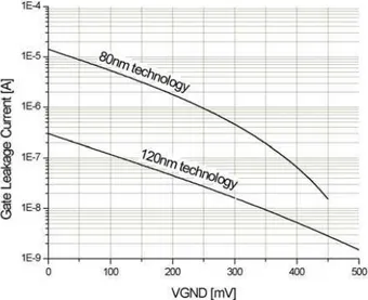
Fig. 4. Gate leakage current in SBVR-CMOS standby mode vs.
voltage on VGND.
5 The 16-T SRAM cell
The large number of transistors in SRAM memories con-tribute to a high total leakage current. On the one hand, the SRAM cell should be fast, and therefore relies on low-vt transistors. On the other hand, leakage current in a big SRAM memory should not exceed a specified range. Special attention must be given to the problem of soft errors (May and Woods, 1978). Low leakage currents and high soft error
GND_L VDD_L
VGND VGND
VVDD VVDD
WL
BLB WL
BL
GND GND
N1
N2 P2 P1
N4 N3
P3 P4
P5 P6 N5 N6 N7
N8 N9
N10 S
SB
pLoad pLoad
Fig. 5. 16-T SRAM cell with low leakage current and high soft
error immunity.
Fig. 6. 16-T SRAM cell showing stable behaviour against alpha
particle attack.
stability should be combined in a modified circuit topology. The novel 16-transistor SRAM cell, as shown in Fig. 5, re-duces the total leakage current by a factor of 200 compared to a common 6-transistor cell (Schmitz, 2002). Read and write performance are not affected. Additionally, its soft error sta-bility, i.e. the critical charge injection before an error occurs, is five times higher than that of a standard SRAM cell.
In standby mode, the 16-T SRAM cell uses two sets of virtual rails for power supply and ground. Thus, most tran-sistors can be kept in accumulation which helps to reduce subthreshold current significantly. Since the absolute drain-source voltage of all transistors is lowered, also DIBL, GIDL, and gate leakage currents are minimized. Simulation results show an overall leakage current reduction of a factor 400 for the 16-T cell when going into sleep mode.
358 A. Schmitz and R. Tielert: Reduced leakage current in Deep Submicron CMOS technologies
6 Conclusion
Large reduction of standby power can be obtained by avoiding some limiting physical effects on transistor level. Conventional CMOS design flows can be used as the basis for the suggested extensions of the proposed technique. The four dominant leakage current phenomena are effectively reduced by SBVR-CMOS. The proposed 16-T cell is an effective replacement for the 6-T SRAM, if both low standby currents and a high soft error stability is required. In radiation-hard applications this cell might be a good choice, despite of the larger cell area.
References
v. Ardenne, M., Musiol, G., and Reball, S.: Effekte der Physik und ihre Anwendungen, Verlag Harri Deutsch, Thun und Frankfurt a. M., 1997.
Chan, T. Y.: The Impact of Gate-Induced Drain Leakage Current on MOSFET Scaling, IEEE IEDM, Technical Digest, 718–721, 1987.
May, T. C. and Woods, W. H.: A new physical mechanism for soft errors in dynamic memories, IEEE Proc. 1978, Int. Reliability Physics Symposium, New York, 1978.
Mutoh S., Douseki T., Matsuya Y., et al.: 1-V Power Supply High-Speed Digital Circuit Technology with Multi-threshold-Voltage CMOS, IEEE Journal of Solid-State Circuits, vol. 30, 847–853, August 1995.
Schmitz, A.: Reduktion des Ruhestroms bei Deep Submi-cron CMOS-Technologien, Dissertation, Technische Universit¨at Kaiserslautern, 2002.
Tsividis, Y. P.: Operation and Modeling of the MOS transistor, McGraw-Hill, New York, 1987.