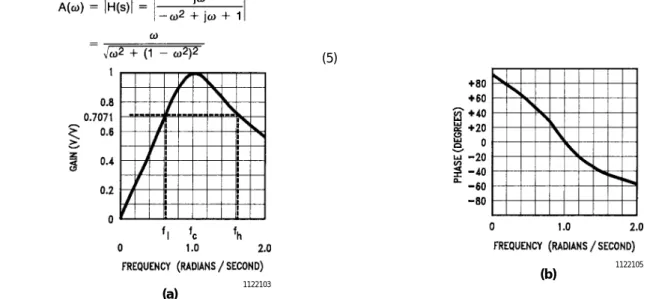
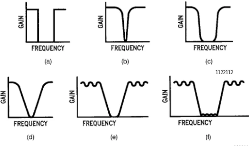
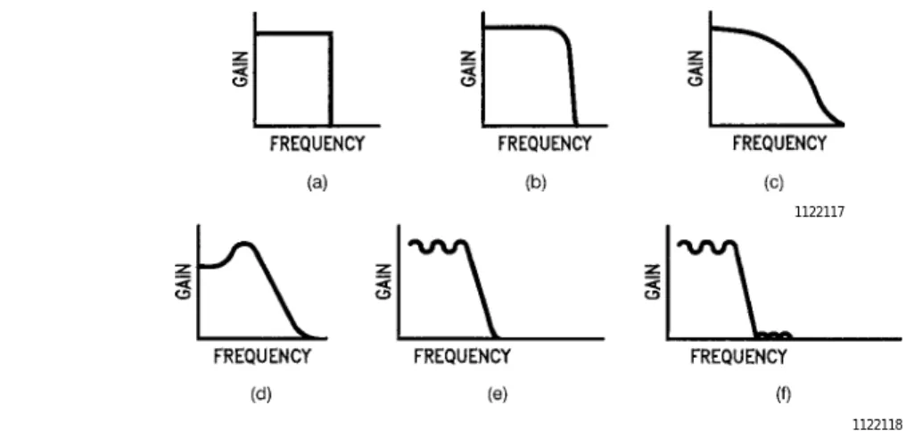
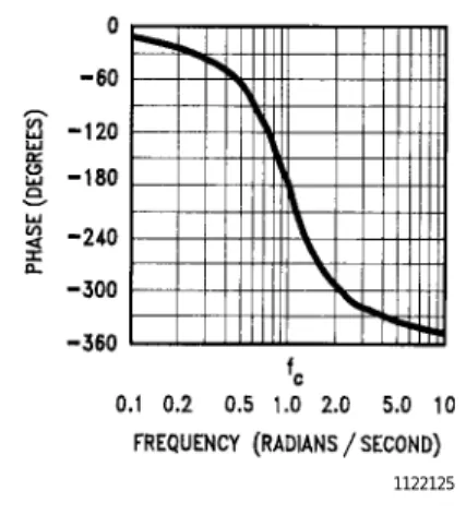
AN 779 National Basic filters
Texto
Imagem


Documentos relacionados
No Gráfico 2, diferente do Gráfico 1, os dados já foram tratados para que o valor de transmissão seja sempre relativo ao da tensão de uma amostra contendo apenas água (equivalente
Para isso é necessário estar atento às novas necessidades de aprendizagem e às suas diferentes formas, o significado do conhecimento no mundo atual, a sua aplicabilidade
À semelhança do que acontecia no período Imperial, para Romanelli (1998), assim se consagrava a falta de diversificação do ensino superior e a concepção aristocrática de ensino.
Poli (líquidos iônicos) (PLIs) e aminas suportadas têm sido apontados como materiais promissores para captura de CO 2.. PLIs combinam as características úteis dos
In contemporary days, there seems to be a growing need to socialize personal problems, and notably, women’s magazines appear to be a good vehicle for sharing
Low-pass filters were applied to monosyllable words con- taining fricative phonemes in the speech samples processed by the frequency and original speech compression algorithm at
Os itens QI Próprio, QI de um Filho, Renda Versão Maior e Atratividade Própria apresentaram maior frequência de escolha significativamente maior pela alternativa posicional ,
Por conseguinte, foi possível desenvolver um instrumento confiável para avaliar a qualidade de serviços de Fisioterapia neuropediátrica com base na percepção de cuidadores,
