DRAFT: An On-line Concurrent Test for
Partial and Dynamically Reconfigurable
FPGAs
Manuel G. Gericota
1, Gustavo R. Alves
1, Miguel L. Silva
2, José M. Ferreira
21
Department of Electrical Engineering
ISEP
Rua Dr. António Bernardino de Almeida, 4200-072 Porto, Portugal
E-mail: {mgg, galves}@dee.isep.ipp.pt
Dep. of Computers and Electrical Engineering
FEUP
Rua Dr. Roberto Frias, 4200-465 Porto, Portugal
E-mail: {mlms, jmf}@fe.up.pt
Abstract
The use of partial and dynamically reconfigurable FPGAs in reconfigurable systems opens exciting possibilities, since they enable the concurrent reconfiguration of part of the system without interrupting its operation. Nevertheless, larger dies and the use of smaller submicron scales in the manufacturing of this new kind of FPGAs increase the probability of failures after many reconfiguration processes. New methods of test and fault tolerance are therefore required, capable of ensuring system reliability.
This paper presents improvements to our RaT Freed Resources technique, originally present in [1], a structural concurrent test approach able to detect and diagnosis faults without disturbing system operation, throughout its lifetime.
1. Introduction
♦
♦
♦
♦
Reconfigurable logic devices, namely Field Programmable Gate Arrays (FPGAs), experienced a considerable expansion in the last few years due in part to its flexibility and to an increase in its size and complexity. The advantages of these devices were considerably reinforced with the advent of a new kind of SRAM-based FPGAs, capable of implementing fast run-time partial reconfiguration (e. g. the Virtex family from Xilinx), enabling the dynamic customization of hardware functions to a
♦ This work is supported by the Portuguese Foundation for Science and Technology (FCT), under contract POCTI/33842/ESE/2000
particular system or application concurrently with system operation.
Unfortunately, as in the rest of the semiconductor industry, current technology tends to make FPGAs less reliable, because smaller submicron scales increase the threat of electromigration, due to higher electronic current density in metal traces. Larger FPGA dies is another factor that increases the probability of failure [2]. Certain defects related to manufacturing imperfections are not large enough to influence initial testing, but they become exposed after large periods of operation, emerging as either stuck-at faults or transient faults [3].
A higher reliability level can therefore only be achieved through the continuous test of all FPGA blocks during the system lifetime, and the introduction of fault tolerance features. This paper presents a structural concurrent test method, which uses the partial and dynamic reconfigurable features introduced by these devices, and the well established IEEE 1149.1 Boundary Scan (BS) test infrastructure [4, 5], thus presenting a very low test overhead at chip and board level. Some simulation results are present for each of the several method phases. Even though the majority of the Look-Up Table (LUT) -based FPGA silicon area is taken up by interconnect requirements, we first focus the fault detection procedures on the LUTs and flip-flops (registers), since they hold the programmable components of the device, and are much more likely to experience faults than metal interconnect wires. Furthermore, the fault detection mechanism proposed here can only be expected to detect persistent faults, which are more likely to occur in the LUTs and registers, since both of these elements
are based on memory cells. However, it can also be used to test interconnections, with Configurable Logic Blocks (CLBs) under test being replaced by wires under test.
In our approach, configuration memory is considered fault free and will not be tested. However, the same test infrastructure could be used to perform a readback of the configuration data that was loaded into the FPGA, helping to detect faults in the configuration elements. A readback and compare software application, capable of performing full readback configuration memory through the Test Access Port, and of comparing the result file with the original configuration file, was developed with this aim.
This paper is organized as follows: recently proposed approaches to the test of SRAM-based FPGAs are first revised, followed by a general description of the structural concurrent test solution envisaged for the CLBs of an FPGA. The next two sections present separately the two components of the proposed solution: the mechanism used to free the CLBs to be tested; and the strategy used to test them. Simulation results are presented in both sections, in order to validate the proposed solution. We conclude this paper by presenting some directions for further research.
2. Background
The test of SRAM-based FPGAs has been addressed in some recent publications, where different manufacturing off-line test methodologies are considered, employing several Built-In Self-Test (BIST) strategies or external test procedures. On-line/functional test methods and structural/ application-oriented tests were also proposed, as referred below, in more recent publications.
An FPGA test approach based on BIST techniques, presented in [6-9], exploits the reprogrammability of FPGAs in order to set up the BIST logic, which exists only during off-line testing. Since the test sequences are a function of the FPGA architecture and not a function of what is programmed into the FPGA, this approach is applicable to all levels of testing (wafer, packaged device, board, and system). Testability is achieved without any area overhead or performance penalty, since the BIST logic is eliminated when the circuit is reconfigured for normal operation.
A slightly different BIST technique, which implies structural modifications on the original configuration memory, is proposed in [10]. When compared to similar BIST techniques, this method reduces test time and the required off-chip memory, while enabling the automation of the test process. The modifications required at the internal hardware level of the FPGA are a main drawback, implying the non-universality of the solution.
An off-line test based on a non-BIST approach, targeted to test the FPGA CLBs, is presented in [11, 12]. After a specific test configuration is set up, the FPGA Input/Output Blocks (IOBs) are used to support the external application of test vectors and to capture the test responses. In order to achieve 100% fault coverage at CLB level, different test configurations are programmed and specific sets of test vectors used in each case.
These approaches are restricted to manufacturing test, since they require the device to be off-line. This is unsatisfactory in highly fault-sensitive, mission-critical applications. Fault-detection latency increases also greatly as a result of an off-line approach.
In order to overcome these limitations, on-line BIST-based test and diagnosis methods BIST-based on a scanning methodology were presented in [3, 13-15]. The idea underlying these methods is to have but a relatively small portion of the chip being tested off-line (instead of the whole chip as in previous proposals), while the rest continues its normal on-line operation. Testing is accomplished by sweeping the test functions across the entire FPGA. If the functionality of a small number of FPGA elements can be replicated on another portion of the device, then those elements can be taken off-line and tested for faults in a transparent manner (i.e. without interrupting the system functionality). This fault scanning procedure then moves on to copy and test another set of elements, sweeping through the whole FPGA, systematically testing for faults.
A different approach specifically devised for LUT -based FPGAs, featuring design for testability characteristics, was proposed in [16]. The automatic incorporation of testability features is achieved by an algorithm that maps optimised Boolean expressions into LUTs, allowing on-line detection of faults within an FPGA. This is accomplished by using a unique set of cells, which operate on the premise of a two-rail checker, thus producing both each output and its complement, when a cell is operating correctly, and two outputs of the same value in the presence of a fault. A fault generated in an intermediate cell is propagated to the primary outputs, thus allowing on-line testability of an FPGA-based system. This method could be considered as an error detection technique rather than a structural or functional test approach, since it does not test the resources of the FPGA, and it does not take into consideration its logic structure (instead it aims to detect the presence of faults in the current application). In a new application, a same defect may or may not be detected, because the faulty resource may now be out of use. If the system is always under reconfiguration, this method could result in an intermittent fault, depending on whether or not a logic function is placed into a faulty resource.
A new application-oriented method that generates a functional test, while considering the logic structure of the FPGA where it is implemented, was proposed in [17]. This method is an off-line field-oriented test to be used in a given application, thus presenting the same drawbacks of the previously referred method. Our concurrent test approach, detailed in this paper, re-uses some of the previous concepts, while adding other innovative aspects, namely the use of a much smaller unit of test – the CLB – thus introducing a negligible overhead at the FPGA level. The use of the BS test infrastructure, already widely used for In-System Programming (ISP), brings the additional benefit of a reduced overhead at board level, since no other resources than those of the FPGA itself are used. Being application-independent, and oriented to test the FPGA structure, it guarantees FPGA reliability after many reconfigurations, thus helping to ensure the correct operation for all applications.
3. The DRAFT method
An FPGA comprises an array of independent CLBs, surrounded by a periphery of IOBs, which are interconnectable by configurable routing resources. In the vast majority of applications, only a part of the FPGA resources is used to implement the desired functional specification. Even when independent hardware blocks dynamically share the same FPGA device (in the case of a dynamically reconfigurable hardware system), 100% usage of its resources is hardly ever achieved, so a few blocks will always be free. Therefore, it is possible to consider a strategy to test temporarily unused blocks, without disturbing system operation, taking advantage of the dynamic and partially reconfigurable features offered by new FPGAs.
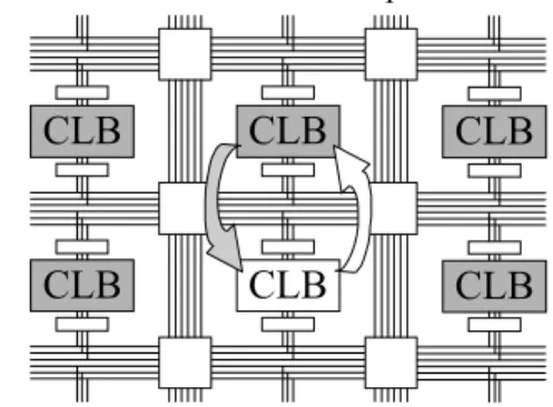
After being successfully tested, unused CLBs remain available as spare parts that may be used to replace other resources found defective. Using a dynamic rotation mechanism, represented in figure 1, CLBs currently being used by a given application can have their functionality replicated in those that were already tested. Both CLBs must remain active with the same state, inputs, outputs, and functionality, for at least one clock cycle, in order to avoid output glitches.
If the currently CLB function is purely combinational, a simple read-modify-write configuration procedure is sufficient to accomplish the replication process. In the case of a CLB implementing a sequential function, the internal state information must be preserved during the replication process. In the FPGA devices belonging to the Virtex FPGA family, it is possible to read the value of a register, but not to perform a direct write operation. Therefore, a temporary transfer path should be established between the registers in the two CLBs, to allow state information to be copied
between them, and at least one clock pulse applied to both, as described in [13]. This solution guarantees that the whole FPGA is tested, without disturbing the system operation, provided that at least one unused CLB is available in the current implementation.
CLB
CLB
CLB
CLB
CLB
CLB
Fig. 1. CLB replication and rotation of free resources
Our proposed DRAFT method (Dynamically Rotate And Free for Test) is controlled through the BS infrastructure, including test application and response capturing, as explained in a later section.
4. The dynamic rotation process
The rotation method used in order to free CLBs for test should have a minimum influence (preferably none) in the system operation, as well as a reduced overhead in terms of reconfiguration cost. This cost depends on the number of reconfiguration frames needed to replicate and free each CLB, since a great number of frames would imply a longer test time and larger memory resources. The impact of this process in the overall system operation is due to variations on circuit timing, originated by changes in routing. Thus, if the re-routing procedure originates a path delay higher than the previous maximum, the maximum frequency of operation is reduced, leading to an undesirable impact in the system operation. Three possibilities were considered for establishing a rule for the rotation of the free CLB, among the entire CLB array: random, horizontal and vertical rotation.The random strategy was rejected for several reasons. If the placement algorithm (in an attempt to reduce path delays) concentrates in the same area the logic needed to implement the components of a given application, it would be unwise to disperse the blocks: firstly, it would generate longer paths (and hence, an increase in path delays); secondly, it would put too much stress in the limited routing resources. Furthermore, a random rotation strategy would imply an unpredictable defect coverage latency, which is not acceptable.
The second strategy, horizontal rotation, is illustrated in figure 2-a). The free CLB would rotate along a horizontal path covering all the CLBs in the array. The replication process would take place
between neighbouring CLBs, due to scarcity of routing resources and to prevent higher path delays. The same rule applies as well to the vertical rotation strategy illustrated in figure 2-b), where the free CLB is rotated along a vertical path.
CLB CLB CLB CLB CLB CLB CLB CLB CLB CLB CLB CLB CLB CLB CLB CLB CLB CLB CLB CLB CLB CLB CLB CLB CLB CLB CLB CLB CLB CLB CLB CLB
a) Horizontal strategy b) Vertical strategy Fig. 2. Dynamic rotation of the free CLB
Simulations performed with the last two strategies, using Virtex Xilinx FPGAs, over a subset of 14 circuits of the ITC’99 Benchmark Circuits from the Politécnico di Torino [18, 19], have shown that the size of the reconfiguration files obtained by the application of the horizontal strategy was approximately 20% higher than the reconfiguration files obtained by the application of the vertical strategy to the same circuit implementations.
The influence of each of the strategies over the maximum frequency of operation was substantially different, mainly due to a pair of dedicated paths per CLB that propagate carry signals vertically to adjacent CLBs [20]. When the rotation process breaks a dedicated carry path, due to the insertion of the free CLB, the propagation of this carry signal between the nearest adjacent CLBs (above and below) is re-established through generic routing resources, increasing the path delay. If the implemented circuit has one or more of these carry signals, the horizontal rotation would break all the carry nets, increasing path delays, but the vertical rotation would break only those in the top or bottom of the CLB columns. So, in this case, and considering only the reduction on the maximum frequency of operation, the vertical strategy is preferable. When no carry signals are present in the implemented circuit, two other factors must be considered: the number of signals with high fanout, and the placement shape (rectangular, square, circular, etc.) and orientation (horizontal, vertical) of the circuits inside the FPGA. Vertical rectangular shape placement implementations perform better with vertical strategy. Instead, the decrease in the maximum frequency of operation is lower with the horizontal strategy in horizontal rectangular shape placement implementations, when many high fanout signals are present. This is the only situation when the horizontal strategy is preferable to the vertical strategy, taking into account only the frequency factor.
Generally, and considering all the 14 circuits, the vertical strategy performs better, with a reduction in the maximum frequency of approximately 7% of its initial value, against 18% found for the horizontal strategy.
After a complete rotation, the initial routing is restored. The scanning process may then be repeated or paused, depending on the overall test strategy.
5. The test session
In order to create the test model of the Virtex CLB structure, some restrictions had to be imposed: • The carry logic would not be tested, because it is not possible to access the CLB carry input and output ports directly (only by passing through the vertically adjacent CLBs);
• The use of LUTs as Distributed RAM would not be initially considered.
Each Virtex CLB comprises two exactly equal slices. One of them, representing the test model, is shown in figure 3. In total, the CLB test model has 13 inputs (test vectors are applied to both slices of each CLB simultaneously) and 12 outputs (6 from each slice). Since the outputs of each slice are captured independently, fault location can be resolved to a single slice. G LUT F LUT ff Y ff X
Fig. 3. Test model of one Virtex slice structure
The BS infrastructure is used to apply test vectors and to capture test responses, with the outputs of the CLB under test (CUT) being routed to unused BS register cells associated to the IOBs. In Virtex devices, all IOBs (bonded and unbonded) are considered as independent 3-state bidirectional pins, in a single BS scan chain, so three BS register bits are provided per IOB. In practice, many of these bits are redundant (depending on the pad configuration), but they are not removed from the scan chain. Using redundant registers to capture the responses, no extra resources are needed for this purpose. However, it is not possible to apply the test vectors through the BS register without affecting the values present at each core logic input, so an alternative User Test Register (UserTR) must be used (the Virtex family enables
the definition of two user registers controlled through the BS infrastructure). This UserTR comprises 13 cells, corresponding to the required number of CLB test configuration inputs. The seven CLBs occupied by this register and the CLB needed to perform the rotation make up for the 0,7% test overhead, computed for the CLB resources of a medium size XCV200 Virtex device. Figure 4 illustrates the implementation of our test procedure.
M U X outputs
User Test Register Bypass register Instruction register Configuration register inputs TDO TDI IOB IOB IOB IOB IOB IOB IOB IOB IOB IOB IOB IOB IOB IOB IOB IOB
. . . .
... ... underCLBtest Fig. 4. Test of a CLBTest vector shifting through the UserTR is very fast, in view of is reduced length. Shifting the response test vector depends on the length of the BS register (device size).
Longer interconnects between the UserTR and the CUT, implying longer path delays, are not a problem due to the low speed limit imposed by the BS infrastructure. However, if routing problems between the UserTR and the CUT occur during the test procedure, its location inside the FPGA may be dynamically changed to a near place, reducing the use of routing resources. The UserTR description must be added to the overall project description in the early stages of the development work. A user constraint file is also provided in order to optimise physical resource allocation for its internal implementation.
Once the UserTR is part of the CLB array, the CLBs where it is implemented are also tested through the same process. This means that all the hardware resources used to implement the test procedure are self-tested.
From our analysis of the Virtex CLB test model structure, we concluded that four test phases are enough to exercise all possible configurations in the CLB. As we did not know the implementation structure of the CLB multiplexers and flip-flops, we considered a hybrid fault model [11]. To test the SRAM elements of the LUT, we set each bit to both 0 and 1. By programming the LUTs (four in each CLB) to implement XOR and XNOR functions –
which requires at least two test phases –, it is easy to propagate any activated faults to a primary CLB output. Due to the XOR/XNOR functions, all LUT input stuck-at faults, together with their respective addressing faults, are also detected. For test purposes, Virtex CLB multiplexers have to be divided in two types: conventional and programmable multiplexers. At least three test configurations are needed to test programmable multiplexers, so a total of four test configurations are enough to completely test the combinational part of the CLB. All flip-flops are tested during these four phases for data input and hold, clock enable, initialise and reverse, and stuck-at’s. Since reconfiguration is slower than vector test application, the small number of test phases is a good measure of our reduced test time. Notice also that test reconfiguration time is not constant through all four phases. In the first test phase, the initial test configuration has to be implemented. In the three subsequent test phases, only a few configuration bits, related to the LUT function and to the programmable multiplexers, are changed. Therefore, test reconfiguration time is smaller. Table 1 details the content of each test session.
Test session
1st test phase 18 test applications 2nd test phase 3 test applications 3rd test phase 2 test applications 4th test phase 16 test applications
Table 1. Contents of a test session
This procedure accounts for 100% fault coverage under the considered fault model.
The back and forth dynamic free-CLB rotation across the chip implies a variable test latency. The time to again reach a given CLB alternates between a maximum and a minimum value (according to the rotation direction), depending on the size of the device.
The maximum fault detection latency is given by ) ( 2 ) 2 ) #
((# rows columns reconf test scanMAX = CLB × CLB − × ×t +t τ
The minimum fault detection latency is in turn given by ) ( 2 reconf test scanmin = × t +t τ where:
treconf: time needed to complete a CLB replication ttest: time needed to test a free CLB
The need to establish a transfer path to allow state information to be copied between the two CLBs involved in the replication process, when the CLB to be replicate is implementing a sequential function, increases the reconfiguration time. Table 2 summarises the timing results obtained applying the DRAFT method to the subset of 14 circuits of the
ITC’99 Benchmark Circuits mentioned before, implemented in a XCV200 Virtex device (array size =28x42 CLBs), at an operation frequency of the BS infrastructure of 32MHz. In this case, the maximum fault latency for the XCV200, assuming that all CLBs implement sequential functions, will be 48 seconds.
treconf+ttest for a CLB implementing a
combinational function 32 ms
treconf+ttest for a CLB implementing a
sequential function 42 ms
Table 2. CLB test time
6. Conclusion
The solution proposed in this paper enables the implementation of a concurrent test method that reuses the standard BS infrastructure and the novel partial dynamic reconfiguration features of recent FPGA devices, in order to improve the reliability of reconfigurable hardware systems, with minimal test overhead and in a way that is completely transparent to the system operation.
In its current form, our approach only addresses local interconnects (inside the CLB and those bringing signals into and out of it), and – in an implicit way –, two other types of interconnects: those used to route test application vectors from the UserTR to the CUT; and those used to route test responses from the same CLB to the Boundary Scan Register. However, interconnect faults will not be recognised as such, being instead detected as CLB faults. The extension of the proposed methodology to test higher level hierarchical switch structures that are not covered by unique CLB faults is under way, and it constitutes one of the steps towards the generalisation of the methodology to test the whole FPGA resources.
Our current work also focuses on the development of computational tools to introduce a higher degree of automation in the whole process. The first of these tools was “Partial Creator”, a software application that produces partial reconfiguration bitstreams from their complete counterparts.
References
[1] Gericota, M. G., Alves, G. R., Ferreira, J. M., “The RaT technique for concurrent test of dynamically reconfigurable hardware”, Proc. of the 15th DCIS
Conf., pp. 337-340, Nov. 2000.
[2] Lach, J., Mangione-Smith, W. H., Potkonjak, M., “Low Overhead Fault-Tolerant FPGA Systems”, IEEE
Trans. on VLSI, Vol. 6, Nº 2, pp. 212-221, June 1998.
[3] Shnidman, N. R., Mangione-Smith, H., Potkonjak, M., “On-Line Fault Detection for Bus-Based Field Programmable Gate Arrays”, IEEE Trans. on VLSI, Vol. 6, Nº 4, pp. 656-666, Dec. 1998.
[4] Hamilton, C., Gibson, G., Wijesuriya, S., Stroud, C., “Enhanced BIST-Based Diagnosis of FPGAs via Boundary Scan Access”, Proc. of the 17th IEEE VLSI
Test Symposium, pp. 413-418, April 1999.
[5] IEEE Standard Test Access Port and Boundary Scan
Architecture (IEEE Std 1149.1), IEEE Standard
Board, October 1993.
[6] Stroud, C., Chen, P., Konala, S., Abramovici, M., “Evaluation of FPGA Resources for Built-In Self-Test of Programmable Logic Blocks”, Proc. 4th Int.
Symposium on FPGA, pp. 107-113, Feb. 1996.
[7] Stroud, C., Konala, S., Chen, P., Abramovici, M., “Built-In Self-Test of Logic Blocks in FPGAs (Finally, A Free Lunch: BIST Without Overhead!)”,
Proc. of the 14th IEEE VLSI Test Symposium, pp.
387-392, April 1996.
[8] Stroud, C., Lee, E., Konala, S., Abramovici, M., “Using ILA Testing for BIST in FPGAs”, Proc. of the
International Test Conf., pp. 68-75, October 1996.
[9] Stroud, C., Wijesuriya, S., Hamilton, C., Abramovici, M., “Built-In Self-Test of FPGA Interconnect”, Proc.
of the International Test Conf., pp. 404-411, Nov.
1998.
[10]Doumar, A., Ohmameuda, T., Ito, H., “Design of an automatic testing for FPGAs”, Comp. of Papers IEEE
European Test Workshop, May 1999.
[11]Huang, W. K., Meyer, F. J., Chen, X., Lombardi, F., “Testing Configurable LUT-Based FPGA's”, IEEE
Trans. on VLSI, Vol. 6, Nº 2, pp. 276-283, June 1998.
[12]Huang, W. K., Meyer, F. J., Lombardi, F., “An approach for detecting multiple faulty FPGA logic blocks”, IEEE Trans. on Computers, Vol. 49, Nº 1, pp. 48-54, Jan. 2000.
[13]Abramovici, M., Stroud, M., Wijesuriya, S., Hamilton, C., Verma, V., “On-Line Testing and Diagnosis of FPGAs with Roving STARs”, Proc. of
the 5th IEEE International On-Line Testing Workshop,
pp. 2-7, July 1999.
[14]Emmert, J., Stroud, C., Skaggs, B., Abramovici, M., “Dynamic Fault Tolerance in FPGAs via Partial Reconfiguration”, Proc. 8th IEEE Symp. on
Field-Prog. Custom Computing Machines, April 2000.
[15]Abramovici, M., Stroud, C., Skaggs, B., Emmert, J., “Improving On-Line BIST-Based Diagnosis for Roving STARs”, Proc. of the 6th IEEE International
On-Line Testing Workshop, July 2000.
[16]Burress, A. L., Lala, P. K., “On-Line Testable Logic Design for FPGA Implementation”, Proc. of the
International Test Conf., pp. 471-478, Nov. 1997.
[17]Renovell, M., Portal, J. M., Faure, P., Figueras, J., Zorian, Y., “Test Generation Optimization for a FPGA Application-Oriented Test Procedure”, Proc. of the
15th DCIS Conf., pp. 330-336, Nov. 2000.
[18]Politécnico di Torino ITC’99 benchmarks, available at http://www.cad.polito.it/tools/itc99.html.
[19]Corno, F., Sonza Reorda, M., Squillero, G., “RT-level ITC’99 benchmarks and first ATPG results”, IEEE
Design and Test of Comp., Vol. 17, Nº 3, pp. 44-53,
July-Sept. 2000.
[20]Gericota, M. G., Alves, G. R., Ferreira, J. M., “Dynamically Rotate And Free for Test: The Path for FPGA Concurrent Test”, 2nd IEEE Latin-American
Test Workshop Digest of Papers, pp. 180-185, Feb.