CAPACITIVE MEMS ACCELEROMETERS TESTING MECHANISM FOR
AUTO-CALIBRATION AND LONG-TERM DIAGNOSTICS
L.A. Rocha
1, L. Mol
2, E. Cretu
3, R.F. Wolffenbuttel
2and J. Machado da Silva
11Dept. of Electrical and Computer Eng., Fac. of Eng. of the U. of Porto, Rua Dr. Roberto Frias, 4200-465 Porto, Portugal 2Dept. Microelectronics, Fac. EEMCS, Delft University of Technology, Mekelweg 4, 2628 CD Delft, The Netherlands
3U. of British Columbia, Dept. Electrical and Computer Eng., 2332 Main Mall, Vancouver, BC, V6T 1Z4 Canada [email protected]
Abstract ⎯ A test technique for capacitive MEMS
accelerometers and electrostatic micro-actuators based on the measurement of pull-in voltages is described. A combination of pull-in voltages and resonance frequency measurements can be used for the estimation of process-induced variations in device dimensions from layout and deviations in material properties from nominal value, which enables auto-calibration. Preliminary measurements on fabricated devices confirm the validity of the proposed technique. Moreover, long-term pull-in measurements have indicated the suitability of the approach as in-system diagnostic tool.
Key Words: BIST, pull-in, calibration
I.
INTRODUCTION
The increasing implementation of Microsystems, containing sensors and actuators, in commercial products calls for simple diagnostics and fault detection mechanisms. Due to the complex nature of microsystems, where multiple energy domains interact at the micro-level, the test mechanisms tend to be complex and cost-intensive. Capacitive accelerometers are among the most commercialized microelectromechanical systems (MEMS) and several built-in self-test (BIST) schemes have been proposed to assure high reliability levels [1-4]. In [1] a simple functional test is performed. An electrical test signal is used to stimulate the device and movement is detected. In [2-4] differential BIST approaches are presented. While the voltage that results from self-test is used to detect asymmetries between capacitors caused by fabrication defects or operational failures [2-3], also a special test signal is used [4].
A more recent approach [5] proposes the use of the current during a pull-in transition to detect possible failures. Pull-in [6] is a unique feature of capacitive MEMS devices and can provide detailed information about their characteristics. Since the electrostatic force due to a field is inversely proportional to the square of the deflection and the restoring force of the beam is, to a first approximation, linear with deflection, an unstable system results in case of a deflection, v, beyond a critical value, vcrit. The pull-in voltage, Vpi, is defined as the voltage that is required to obtain this critical deflection and depends mainly on dimensions, residual stress level and design, which makes it ideal to characterize structural materials in surface micromachining processes [7,8]. Unlike the case of the comb drive, which is based on area-varying capacitors, the design of most electrostatic actuators relies on gap-width
varying capacitors and the pull-in phenomenon has to be considered [9]. Pull-in causes the displacement range due to electrostatic force to be limited to 1/3 of the gap between the electrodes, in case of a motion perpendicular to the capacitor plate orientation.
In this paper the use of the pull-in voltage as a test parameter is proposed. When pull-in voltage measurements are combined with the measurement of the resonance frequency (a single measurement is needed), the fabrication process non-idealities like over-etching and process asymmetries can be estimated. Consecutive pull-in voltage measurements can be used to make accurate diagnostics as well as to perform electronic calibrations.
II.
PULL-IN VOLTAGE
The simplest symmetric micromechanical system suitable for studying the pull-in voltage is composed of three electrodes, one movable and connected to a suspension beam with a certain spring constant k (Fig. 1a) and the other two fixed on a rigid supporting substrate. This is often the case of capacitive accelerometers, which have separate electrodes for sensing and actuation.
Figure 1. Sketch of the basic device with a) ideal conditions and b) with over-etch and asymmetries
For a global stable equilibrium in such a microsystem, the second derivative of the potential energy of the system with respect to deflection should be positive:
2 2 0 p U x ∂ > ∂ , thus the pull-in voltage (Vpi) results from
2 2 0 p U x ∂ = ∂ and is determined by the beam material, the beam dimensions, residual stress, and the electrodes dimensions (electrostatic energy). The residual stress should not affect Vpi and therefore the beam should be suspended using folded tethers at each end [10]. This approach ensures that the built-in strain energy component caused by longitudinal stress is negligible. Due to the symmetry of the structure three pull-in voltages can be defined as shown in Fig. 1a: asymmetric-right (Vpr), asymmetric-left (Vpl) and symmetric (Vps). Assuming ideal conditions, analytical expressions for the three pull-in voltages can be found [6]:
3 0 0 3 0 0 8 27 1 2 pr pl s d k V V wl d k V wl ε ε = = = , (1)
where d0 is the capacitor initial gap, k is the mechanical spring, ε0=8.8546x10⁻¹² is the air permittivity and w and l are the capacitor plate width and length, respectively. If non-ideal process conditions are now considered (Fig. 1b) like over-etching [11], capacitor gap mismatch and Young’s Modulus (E) value deviations, the pull-in voltage values will vary, making them suitable to estimate the non-idealities and to be used as a diagnostic mechanism.
III.
PROPOSED TEST SCHEME
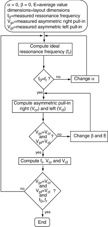
Since pull-in is an intrinsic property of microelectromechanical systems, it is an ideal test mechanism. Fabricated devices often exhibit actual dimensions smaller than the designed ones (due to over-etch). Over-etching can be considered uniform along the microfabricated device [11], which means that all layout dimensions will be affected by the same parameter α. This will have a uniform effect on all three pull-in voltages. Small gap mismatches (a few nm) are also observed in fabricated devices. In this case, the gap mismatch (β) will affect differently the three pull-in voltages and therefore it becomes easy to estimate β from the differences between
Vpl and Vpr. The parameter α is more difficult to estimate, because there is an extra unknown parameter: the Young’s Modulus (its average value is known, but it can show large deviations). If we introduce a new measurement, the resonance frequency, both α and E can be estimated and a clear description of the mechanical device is achieved. A flow chart of he proposed scheme is shown in Fig. 2. After this initial estimation, the parameters susceptible of changing with aging and device operation are the Young’s Modulus and the gap mismatch [12], while the structure dimensions remain constant. This implies that consequent pull-in measurements are an excellent diagnostic
parameter. Since the sensitivity of the device is known, test signals can also be applied to the actuation capacitors to calibrate the full system (device plus readout electronics). One disadvantage of the proposed technique is that it relies on very accurate device models that can predict the device electro-mechanical behavior. These models have to incorporate all the non-idealities existing in the micro-domain, like capacitor fringe fields and residual stress, which makes the modeling one of the critical parts of the proposed test scheme.
Figure 2. Flow chart to estimate α,β and E from measurements
IV.
METHOD EVALUATION
Accelerometers fabricated within the Bosch epi-poly process [13] were used to test the proposed test scheme. A drawing of the device used is depicted in Fig. 3.
Figure 3. Drawing of the accelerometer IV.1 MECHANICAL DOMAIN
The mechanical spring of the structure is composed of 4 folded beams. Assuming that the trusses joining the folded-beam segments are rigid, an approximate analytical expression (this expression assumes that the end of the beam can freely rotate which is not the case) for k can be found [14]: 3 3 3 2 ( ) 8 2 2 ( 2 ) EI b k Eh L L α α α α − = = + +
⎛
⎞
⎜
⎟
⎝
⎠
, (2)where: I =h b( −2 ) /12α 3 is the moment of inertia of the beams, E is the Young’s Modulus, α is the over-etch parameter and h, b and L are the thickness, width and length respectively of each beam. A finite-element model (FEM) reveals that this expression over-estimates in 4% the actual mechanical spring.
IV.2 ELECTRICAL DOMAIN
The device under study has 12 actuation capacitors. The total electrostatic energy can be written as (neglecting fringe fields): 2 2 0 1 1 ( 2 ) ( ) 12 ( ) 12 2 2 2 elect w l U C V V d α α = α = ε − α +
,
(3) where d is the capacitor gap distance, w (thickness of the mechanical layer) is the capacitor width and l is the capacitor length. Considering now the fringe fields, and assuming that the length of the electrodes l, is large when compared with width w and distance d, the fringe field contribution from the ends of the plate can be neglected when compared to the fringe field that results from the width of the plate. In that case an expression for the total capacitance can be found:0 1 12 w 1 ln 2 w C l d d ε π π ⎛ ⎛ ⎛ ⎞⎞⎞ = ⎜ + ⎜ + ⎜⎝ ⎟⎠⎟⎟ ⎝ ⎠ ⎝ ⎠
.
(4)The total electrostatic force, including fringe fields is:
2 2 0 2 1 112 1 2 2 e C w F V lV d ε d πd ∂ ⎛ ⎞ = = ⎜ + ⎟ ∂ ⎝ ⎠
.
(5)Although these analytical equations are very accurate, the fringe fields are very difficult to quantify and usually numerical methods (FEM) have to be used. Since modeling is an important part of the method, capacitive FEM simulations for changing α were computed and compared with C( )
d α
∂
∂ . Comparative results are shown in Fig. 4 and a small deviation between models can be noticed. The analytical model under-estimates the effect of the fringe fields (about 10%).
Figure 4. Comparison between FEM model and analytical models
IV.3 FABRICATED DEVICES
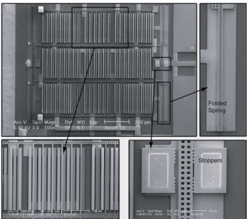
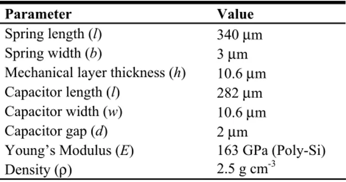
The fabricated accelerometers (Fig. 5.) are composed of four folded springs, 340 μm long and 3 μm wide (layout dimensions), connected to two rigid central bars of about 1mm long. Parallel-plate capacitors with a 2 μm gap are used for actuation. The displacement measurement involves sensing the changes of various sets of differential capacitors. The main device layout parameters and bulk material properties are shown in Table 1.
Table 1. Main nominal parameters of the device (layout dimensions and bulk material mean values)
Parameter Value Spring length (l) 340 μm
Spring width (b) 3 μm Mechanical layer thickness (h) 10.6 μm Capacitor length (l) 282 μm Capacitor width (w) 10.6 μm Capacitor gap (d) 2 μm
Young’s Modulus (E) 163 GPa (Poly-Si) Density (ρ) 2.5 g cm-3
IV.4 EXPERIMENTAL RESULTS
Several devices fabricated on the same run were tested. The resonance frequency does not show big variations from device to device (less than 1% changes), while the three pull-in voltages showed substantial differences. A set of measurements is presented in Fig. 6 and Table 2 presents experimental values for two different devices.
Figure 6. Pull-in measurements
Table 2. Pull-in and resonance frequency measured values Parameter Value Asymmetric right - Vpr 3.93V Asymmetric left - Vpl 3.67V Symmetric - Vs 4.5V Device 1 Resonance Frequency – f0 2740 Hz Asymmetric right - Vpr 3.84V Asymmetric left - Vpl 3.74V Symmetric - Vs 4.72V Device 2 Resonance Frequency – f0 2740 Hz If the algorithm of Fig. 2 is applied to the set of values presented in Table 2, the values for α, β and E can be estimated. Table 3 presents the estimated values. The symmetric pull-in does not contribute with extra information, but can be used to confirm the estimated values for α, β and E.
Table 3. Estimated α, β and E values and simulated pull-in voltages and resonance frequency
device α β E 1 252nm 56nm 144.9 GPa 2 250nm 21nm 144.3 GPa device Vpr Vpl Vs f0 1 3.926V 3.675V 4.499V 2722 Hz 2 3.84V 3.745V 4.713V 2718 Hz
IV.5 METHOD VERIFICATION
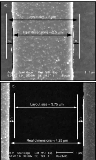
The results presented in Table 3 are very promising and the good agreement between α and E values for the devices (that should be very similar since they were fabricated in the same run) show that the deviations on the pull-in voltages are caused by gap mismatches (β). Those have to do with lateral gradient stresses that often are neglected, or with over-etch asymmetries that originate small deviations in the gaps (on the order of a few nm). To verify these results, some devices were observed at the SEM microscope to check if the device dimensions showed an over-etching of about half a micron (α=250nm). Two illustrative SEM images are shown in Fig. 7.
The SEM images revealed that the devices present an over-etching very close to the one obtained after the test method. This very good agreement proves that pull-in voltage measurements can be used to accurately estimate process deviations and device performance.
IV.6 DISCUSSION
Like several other MEMS test techniques, the proposed test scheme uses a variable electrical signal to stimulate the device, and the device response can be used to obtain very important device information and most of all to obtain confidence on device functionality (a damaged device will present no pull-in behavior). So far it has been shown that with this technique the device performance can be fully characterized, but that is not enough to achieve a full BIST technique.
In order to achieve a full BIST technique, on-chip test circuits must be integrated for generating the necessary electrical signals for actuating the device and analyzing the responses. Before proposing an on-chip test method, long- term measurements must be performed to check and correlate known failure mechanisms with long term pull-in deviations. First results prove that the differences between expected pull-in voltages (using layout dimensions) and measured pull-in voltages can be explained from fabrication (over-etch, gap mismatches and Young’s Modulus deviations). We expect that long-term measurements will be able to give us information on device failures through shifts in the pull-in voltages, and it is likely that different failure modes will present different pull-in deviations in time.
Figure 7. SEM photographs of a a) folded beam and b) capacitor gap at the stopper
Another advantage of this technique is the fact that it can be used to electrically calibrate an accelerometer. Normal accelerometer calibration (as an example we consider a ±1g accelerometer) is done by applying a 1g acceleration followed by a -1g acceleration (putting the sensitivity axis along the earth gravity field) while checking the response. Usually this is done manually and it is not a good solution for remotely placed sensors or sensors of difficult access. Since a very accurate model is obtained with the proposed scheme, the actuation voltages that give the same response as a ±1g can be computed and used to electrically calibrate the sensor.
V.
CONCLUSIONS AND FUTURE
WORK
A novel test technique based on pull-in voltages was presented and preliminary results show the feasibility of the method. The very good agreement between measured values, measured dimensions and simulations, confirm the validity of the MEMS models used and the potential of the technique.
Long-term pull-in measurements are on-going and pull-in deviations from the initial measured values are expected to give information on device performance deterioration and to identify or differentiate between failure modes.
Future work includes failure mode identification based on pull-in voltage deviations and estimation of errors due to uncertainty on the measurements and how those can influence on the correct estimation of the device parameters.
REFERENCES
[1] H. V. Allen, S. C. Terry, and D. W. de Bruin, “Accelerometer systems with self-testable features,” Sens. Actuators, vol. 20, pp. 153–161, 1989.
[2] N. Deb and R.D. Blanton, “Buil-In Self Test of CMOS-MEMS Accelerometers” Proceedings of International Test Conference, pp. 1075-1084, 2002. [3] N. Deb and R.D. Blanton, “Multi-Model Built-In
Selft-Test for Symmetric Microsystems” Proceedings of VLSI Test Symposium, pp. 139-147, 2004.
[4] X. Xiong, Y.L. Wu and W.B. Jone, “A Dual-Mode Built-In Self-Test Technique for Capacitive MEMS Devices” Proceedings of VLSI Test Symposium, pp. 148-153, 2004.
[5] B. Caillard, Y. Mita, Y. Fukuta, T. Shibata and H. Fujita, “A Highly Simple Failure Detection Method for Electrostatic Microactuators: Application to Automatic Testing and Accelerated Lifetime Estimation”, IEEE Trans. Semiconductor Manufacturing, vol. 19, pp. 35-42, 2006.
[6] L.A. Rocha, E. Cretu and R.F. Wolffenbuttel, “Analysis and Analytical Modeling of Static Pull-In With Application to MEMS-Based Voltage Reference and Process Monitoring”, J. Microelectromech. Syst., vol. 13,pp. 342-354, 2004.
[7] S. T. Cho, K. Najafi, and K. D. Wise, “Internal stress compensation and scaling in ultra-sensitive silicon pressure sensors,” IEE Tr. ED, vol. 39, pp. 836–842, 1992.
[8] P. M. Osterberg and S. D. Senturia, “M-TEST: a test chip for MEMS material property measurement using electrostatically actuated test structures,” J. Microelectromech. Syst., vol. 6, pp. 107–118, 1997. [9] H. A. C. Tilmans and R. Legtenberg, “Electrostatically
driven vacuum encapsulated polysilicon resonators, part 2, theory and performance,” Sens. Actuators, vol. A45, pp. 67–84, 1994.
[10] W. C. Tang, T.-C. H. Nguyen, and R. T. Howe, “Laterally driven polysilicon microstructures,” Sens. Actuators, vol. A20, pp. 25–32, 1990.
[11] J.V. Clark, D. Garmire, M. Last, J. Demmel and S. Govindjee, “Practical Techniques for Measuring MEMS Properties”, Proceedings Nanotech 2004, vol. 1, pp. 402-405, 2004.
[12] M. T.-Azar, K. Wong and W. Ko , “Aging phenomena in heavily doped (p+) micromachined silicon cantilever beams”, Sens. Actuators, vol. A33, pp. 199–206, 1992. [13] http://www.bosch-sensortec.com.
[14] J. M. Gere and S. P. Timoshenko, Mechanics of Materials; Third SI Edition. London, U.K.: Chapman and Hall, 1991.