Diogo Miguel de Castro Madeira Fernandes
[Nome completo do autor]
[Nome completo do autor]
[Nome completo do autor]
[Nome completo do autor]
[Nome completo do autor]
[Nome completo do autor]
[Nome completo do autor]
Licenciado em Ciências de Engenharia de Materiais
[Habilitações Académicas] [Habilitações Académicas] [Habilitações Académicas] [Habilitações Académicas] [Habilitações Académicas] [Habilitações Académicas] [Habilitações Académicas] Outubro, 2019
Lithiation and Characterisation by Ion Beam
Techniques of V
2O
5Thin Films
[Título da Tese] Dissertação para obtenção do Grau de Mestre em Engenharia de Materiais
Dissertação para obtenção do Grau de Mestre em
[Engenharia Informática]
Orientador: Doutora Joana Vaz Pinto Sarmento,
Professora Auxiliar Convidada, (DCM) FCT/UNL Co-orientadores: Doutor João Cruz,
Professor Auxiliar, (DF) FCT/UNL
Júri:
Presidente: Doutor Alexandre José da Costa Velhinho,
Professor Auxiliar, (DCM) FCT/UNL Arguentes: Doutor Luís Miguel Nunes Pereira,
Professor Associado, (DCM) FCT/UNL Vogais: Doutora Joana Vaz Pinto Sarmento,
Lithiation and Characterisation by Ion Beam Techniques of V2O5 Thin Films
Copyright © Diogo Miguel de Castro Madeira Fernandes, Faculdade de Ciências e Tecnologia, Universidade Nova de Lisboa, 2019.
A Faculdade de Ciências e Tecnologia e a Universidade Nova de Lisboa têm o direito, perpétuo e sem limites geográficos, de arquivar e publicar esta dissertação através de exemplares impressos reproduzidos em papel ou de forma digital, ou por qualquer outro meio conhecido ou que venha a ser inventado, e de a divulgar através de repositórios científicos e de admitir a sua cópia e distribuição com objetivos educacionais ou de investigação, não comerciais, desde que seja dado
Acknowledgements
I would like to use this section to express my gratitude towards everyone involved in the completion of this work. Firstly, an acknowledgement to CENIMAT and CTN/IST for providing an excellent environment and the conditions required for the elaboration of this thesis.
I am extremely grateful to my supervisor Dra. Joana Vaz Pinto Sarmento for her patience, availability and consistent guidance throughout the entirety of the work. Her enthusiasm was highly motivating and kept me optimistic throughout.
To my co-supervisor Dr. João Cruz, I thank him for introducing me to the subject of nuclear reactions and teaching me the fundamentals. His knowledge on the subject was inspiring and the visits to CTN with him were an unforgettable experience.
I would like to thank the remainder of my thesis committee: Prof. Alexandre Velhinho and especially Prof. Luís Pereira for their encouragement, understanding and insightful perspectives.
I thank the staff and professors at CENIMAT and CEMOP: Alexandra Gonçalves, Dr. Ana Pimentel, Inês Cunha and Dra. Rita Branquinho for the training, education and suggestions for the laboratory work. In particular, I am grateful to Sónia Pereira for her valuable insights and proof-reading, as well as assistance and discussions on the work.
I would like to give an acknowledgement to the members and staff at CTN: Jorge Rocha, Dr. Luís Alves, Dr. Rodrigo Mateus and Dr. Rui Silva for their insight on nuclear reactions.
A special thank you to my friends at FCT: Bernardo Sarmento, Joana Raminhos and Tomás Freire for sticking with me throughout our university journey and for pushing me to be better.
Lastly, I would like to express my profound gratitude towards my parents for their caring, encouragement and support throughout my years of study. Thank you.
Abstract
In this work, studies on the mechanism of lithium ion intercalation (Li+) in vanadium pentoxide thin films (V2O5) were performed. The intercalation was induced by electrochemical experiments and the conditions and parameters used were optimised to allow structural, optical and electrical characterisation. Rutherford Backscattering Spectrometry (RBS) and Nuclear Reaction Analysis (NRA) ion beam techniques, performed at the Centre for Nuclear Technologies (CTN/IST), were used to locate and quantify the presence of Li+ ions in the crystalline structure of the material. In addition, the effect of pre-lithiation by ion implantation on V2O5 thin films was studied.
V2O5 thin films were deposited by electron beam assisted evaporation (EBPVD) on glass substrates with an ITO layer. The samples were subjected to cyclic voltammetry (CV) and chronoamperometry (CA) as a procedure for intercalating Li+ ions in the V2O5 structure. Optical characterization by visible spectroscopy revealed a recovery of the film’s initial transmittance state after the sample was subjected to five cycles of CV. The corresponding I(V) curves displayed a comparable symmetry of peak anodic and cathodic currents indicating reversibility of Li+ intercalation. The X-Ray Diffractograms (XRD) of these samples showed the presence of an orthorhombic structured V2O5 with a preferential orientation in the (0 0 1) plane. The intercalation resulted in an increase in interplanar spacing of 3% along the lattices’ c-axis, which varied proportionally with the applied voltage. RBS and NRA spectra revealed distinct peaks, characteristic of 7Li+ ions and it was possible to quantify Li as an atomic percentage of the samples’ composition along its depth. It was also observed that the depth profile for Li extended beyond the ITO layer. The electro-optical characterisation of Li+ ion implantation found a reduction in the samples’ intercalation reversibility, with depth profiles suggesting Li entrapment.
It was possible to quantify and detect the presence of Li+ ions and correlate these results with the structural expansion induced by the intercalation.
Resumo
Neste trabalho, foram realizados estudos sobre o mecanismo da intercalação de iões de lítio (Li+) em filmes finos de pentóxido de vanádio (V2O5). A intercalação foi induzida por experiências eletroquímicas e as condições e parâmetros utilizados foram otimizados para possibilitar caracterizações estruturais, óticas e elétricas. As técnicas de feixe de iões espectrometria de retrodispersão de Rutherford (RBS) e análise de reações nucleares (NRA), efetuadas no Centro de Tecnologias Nucleares (CTN/IST), foram utilizadas para localizar e quantificar a presença de iões de Li+ na estrutura do material. Adicionalmente foi estudado o efeito da pré-litiação no V2O5 efetuada pela técnica da implantação iónica.
Os filmes de V2O5 foram depositados por evaporação térmica por feixe de eletrões (EBPVD) em substratos de vidro com uma camada de ITO. As amostras foram submetidas às técnicas de voltametria cíclica (CV) e cronoamperometria (CA) para intercalar iões de Li+ na estrutura do V2O5. A caracterização ótica por espectroscopia do visível revelou uma recuperação da transmitância inicial após as amostras terem sido submetidas a cinco ciclos de CV. As curvas I(V) correspondentes exibiram uma simetria comparável das correntes de pico nos sentidos anódicos e catódicos, que indicou reversibilidade da intercalação de Li+. Os difratogramas de raios X (DRX) mostraram a presença de um V2O5 de estrutura ortorrômbica com orientação preferencial no plano (0 0 1). A intercalação resultou no aumento do espaçamento interplanar de 3% ao longo do eixo c da rede cristalográfica, que variou proporcionalmente com a tensão aplicada. Os espectros de RBS e NRA revelaram picos distintos, característicos dos iões 7Li+ e foi possível quantificar Li como uma percentagem atómica da composição das amostras ao longo da profundidade. Foi também verificado um prolongamento de Li para além do V2O5 no perfil de profundidade da amostra. A caracterização eletro-óptica das amostras implantadas deu uma intercalação menos reversível, os perfis de profundidade foram sugestivos de um aprisionamento de Li.
Foi possível quantificar e detetar a presença de iões de Li+ e correlacionar estes resultados com a expansão estrutural induzida pela intercalação.
TABLE OF CONTENTS
Acknowledgements ... i
Abstract ... ii
Resumo ... iii
TABLE OF CONTENTS ... iv
List of Tables ... vi
List of Figures ... vii
List of Abbreviations and Symbols ... x
Motivation and objectives ... xi
1.
Introduction ... 1
1.1. Vanadium Oxides ... 1
1.2. Lithium Intercalation and Electrochromism in V2O5 ... 2
1.3. Lithiation and Detection of Li by Ion Beam Techniques ... 3
2.
Materials and Methods ... 4
2.1. Vanadium Oxide Deposition ... 4
2.2. Surface Treatments and Characterisation ... 4
2.3. Structural Characterisation ... 4
2.4. Optical and Electrochemical Characterisation ... 4
2.5. Ion Beam Techniques ... 5
2.5.1. RBS and NRA ... 5
2.5.2. Ion Implantation ... 6
3.
Results and Discussion ... 7
3.1. Crystallisation of V2O5 Thin Films: A Structural Characterisation ... 7
3.2. Lithium Intercalation by Electrochemical Processes ... 8
3.2.1. Optical Characterisation of V2O5 Films ... 8
3.2.2. Electrochemical Characterisation of V2O5 Films ... 10
3.2.3. Electro-optical Characterisation ... 11
3.2.4. Combined Structural and Electro-optical Measurements... 13
3.2.5. Quantification of Li+ Ions by RBS and NRA Techniques ... 15
3.3. Ion Implantation of Lithium ... 17
3.3.1. Structural Characterisation ... 18
4.
Conclusions and Future Perspectives ... 23
5.
References ... 24
6.
Appendix ... 28
6.1. Appendix A – Structural Characterisation ... 28
6.2. Appendix B – Optical and Electro-optical Characterisation ... 28
List of Tables
Table 1 - Electrochromic parameters obtained from chronoamperometric
measurements. The parameters obtained for λ3 = 550 nm are highlighted. ... 13 Table 2 – 7Li and total Li quantities and C-axis interplanar distance for the respective
voltages, detected by RBS and NRA in the six-electrode sample. ... 17 Table 3 – 6Li, 7Li and total Li quantities for each sample in the ion implantation
experiment, detected by RBS and NRA. The labels 1, 2 and 3 correspond to the RBS
List of Figures
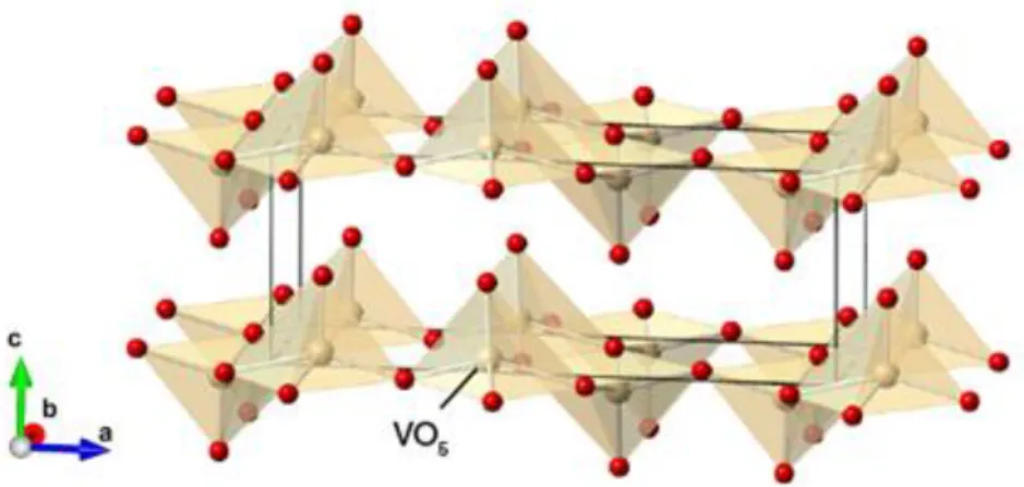
Figure 1 – Representation of the crystalline structure of V2O5. It consists of linked VO5 square base pyramidal units. V atoms are represented as grey spheres, O atoms as red
[38]. The reference axes indicate the lattice parameters. ... 1 Figure 2 – a) Scheme of a two electrode setup. The arrows indicate the direction of
charge carrier flow during intercalation in to the electrochromic material, deposited on the WE [43]; b) Cyclic voltammogram obtained from applying a voltage sweep and
measuring the electric current between electrodes over the course of multiple cycles. ... 2 Figure 3 – Two electrode setup for electrochemical processes: a) Initial setup with front
view of the sample. The yellow V2O5 film is exposed to a circular area (0,883 cm2) of electrolyte. The green wire (1) is connected to the working electrode (ITO) and the red (2) to the counter electrode (Pt wire), submersed in electrolyte; b) Complete setup for electro-optical measurements. The optical fibres are aligned with the circular areas
where the thin film is exposed to electrolyte. ... 4 Figure 4 – a) Scheme of the Danfysic Ion Implanter at LATR/CTN and b) photograph of
the target chamber. The samples are attached to the round metal support. ... 6 Figure 5 – a) RBS chamber with three detectors and the sample holder inserted, b) RBS
line setup and c) Diagram of the Van de Graaf Accelerator... 5 Figure 6 – In-situ XRD analysis of VOx films: a) XRD scans at different filament
temperatures and b) a close-up of the same XRD analysis in the 19º - 22º 2Theta range
for the high-end temperatures ... 7 Figure 7 – XRD scan of annealed sample in the furnace at 450 ºC ... 8 Figure 8 - Optical characterisation of V2O5 and ITO thin films: a) Transmittance spectrum
of in the 250 nm to 700 nm wavelength interval (UV-VIS region) and b) the
corresponding Tauc plot used for extrapolating the optical band gap ... 9 Figure 9 – a) Cyclic voltammograms showing the effect of scan rate on the redox
reactions of V2O5 thin films ; b) Cyclic voltammogram of a V2O5 film at a scan rate of 100
mV/s. The arrows denote the scan direction. ... 10 Figure 10 - V2O5 optical transmittance in the UV-Vis-NIR spectral regions ... 11 Figure 11 - a) Optical transmittance for wavelengths λ1, λ2, λ3 and λ4 over five CV cycles.
The letters c and b denote coloured and bleached, respectively. ; b) The corresponding CV cycles of the V2O5 film at a scan rate of 100 mV/s and ±3 V voltage range. The
arrows denote the scan direction. ... 12 Figure 12 – Optical transmittance for wavelengths λ1, λ2, λ3 and λ4 over five repeating
chronoamperometry scans. The letters c and b denote coloured and bleached,
respectively. ... 12 Figure 13 – XRD scans of a V2O5 sample after each applied voltage in the 2Theta =
Figure 14 – Ex-situ XRD scans of a six-electrode configuration sample: a) XRD scans in the 2Theta 18 to 21.5º range and b) the corresponding interplanar distance (crystallographic c parameter) of the V2O5 in each electrode. The red markers indicate
the values obtained for non-intercalated V2O5. ... 15 Figure 15 – a) RBS spectrum of the electrode biased with -3 V, showing the more
abundant elements present in the sample, b) NRA spectrum of the measured electrode and c) graphic representation of 7Li atomic percentage as a function of depth obtained
by fitting the spectra. ... 16 Figure 16 – MonteCarlo SRIM simulated 7Li+ implantation profiles on a V2O5 layer
deposited over In2O3: a) Li+ ion depth distribution for three different fluencies and b) Visual simulation of the 7Li+ ion implantation on the V2O5/In2O3 layers. Image taken from
the SRIM software. ... 18 Figure 17 – XRD analysis of the samples in the ion implantation chapter with: a) Full
2Theta range of the scan (10º to 50º) and b) Inset graph of the highest intensity peak
within a 2Theta = 18.5º to 21.5º range. ... 18 Figure 18 - XRD analysis of the amorphous samples in the ion implantation chapter 3.3. ... 19 Figure 19 – Optical transmittance of the sample c-V2O5(Li): a) in the UV-Vis-NIR spectral
region, showing different coloured and bleached cycles and b) Wavelengths λ1, λ2, λ3 and λ4 over five repeating chronoamperometry scans. The letters c and b denote coloured
and bleached, respectively... 19 Figure 20 – Optical transmittance of the sample a-VOx(Li): a) in the UV-Vis-NIR spectral
region, showing overlapped coloured and bleached cycles and b) Wavelengths λ1, λ2, λ3 and λ4 over five repeating chronoamperometry scans. The letters c and b denote
coloured and bleached, respectively. ... 20 Figure 21 – a) Graphic representation of 7Li atomic percentage as a function of depth, for
the samples subjected to ion implantation and b) photograph of the sample holder in the
Van de Graaff accelerator’s RBS line. ... 21 Figure 22 - XRD scans of annealed samples in the muffle furnace at 450 ºC and 500 ºC ... 28 Figure 23 - V2O5 optical transmittance in the UV-Vis-NIR spectral regions for each
biased electrode. ... 28 Figure 24 - Optical transmittance of the sample c-V2O5: a) in the UV-Vis-NIR spectral
region, showing overlapped coloured and bleached cycles and b) Wavelengths λ1, λ2, λ3 and λ4 over five repeating chronoamperometry scans. The letters c and b denote
coloured and bleached, respectively. ... 29 Figure 25 - RBS spectrum of the electrode biased with -0.5 V and b) NRA spectrum of
the measured electrode. ... 29 Figure 26 - RBS spectrum of the electrode biased with -1.0 V and b) NRA spectrum of
the measured electrode. ... 30 Figure 27 - RBS spectrum of the electrode biased with -1.5 V and b) NRA spectrum of
Figure 28 - RBS spectrum of the electrode biased with -2.0 V and b) NRA spectrum of
the measured electrode. ... 30 Figure 29 - RBS spectrum of the electrode biased with -2.5 V and b) NRA spectrum of
List of Abbreviations and Symbols
CA Chronoamperometry
CE Counter electrode
CEff Colour efficiency
CTN Centro de Tecnologias Nucleares
CV Cyclic voltammetry
d Interplanar distance
EBPVD Electron-beam physical vapour deposition
EC Electrochromic
ERDA Electron recoil detection analysis
IST Instituto Superior Técnico
ITO Indium tin oxide
LATR Accelerator and Radiation Technologies Laboratory n Transition index (optical characterisation)
n Order of diffraction (structural characterisation)
NRA Nuclear reaction analysis
RBS Rutherford backscattering spectrometry
Redox Oxidation-reduction RF Radiofrequency tb Bleaching time tc Colouration time Tb Bleached transmittance Tc Coloured transmittance
TCO Transparent conducting oxide
WE Working electrode
XRD X-ray diffraction
λ Wavelength
ΔOD Optical density
ΔT Transmittance variation
Motivation and objectives
The increased awareness on environmental issues has resulted in a greater demand of energy saving applications and materials. Smart windows, batteries, sensors, displays, electrochromic devices and catalysts are some examples of applications that have been a focus for development to meet these demands [1–4]. Ion intercalation is a mechanism common to all these applications that rely on charge movement for their functions. It consists of the chemical insertion of a molecule or ion in to an oxide host matrix [5]. Therefore, to promote and control the ion movement and diffusion of ions between the ion source and the matrix, it is of great importance to acquire knowledge on how to optimize the performance of these applications. Electrochromism was a specific focus of this study as it is a phenomenon that presents visible evidence of intercalation: a reversible change in colour. The most commonly studied materials in this field include NiO, V2O5 and most notably WO3 that exhibits good stability and transmittance modulation in the infrared spectral region [6–10]. Of these, V2O5 was considered of high interest since its intercalation mechanism is also prominent in Li-ion batteries as a cathode due to its high capacity, low cost and abundance [11–15]. Lithium on the other hand is the most popular choice as charge carrier as it contributes to a high density energy and lightweight configuration [16,17].
Typical electro-optical measurements performed to test electrochromism indicate charge insertion and a corresponding transmittance variation. However these measurements have a limitation in that charge quantities are estimated by current-voltage responses [18] and the location of the ions within a typical two-electrode setup is not obtainable by these methods. Analytical techniques such as scanning electron microscopy (SEM), x-ray fluorescence (XRF) and x-ray photoelectron spectroscopy (XPS) are used to measure elemental compositions; however, Li phases have proven to be problematic to identify [19,20]. Ion beam techniques such as RBS and NRA can be used to measure light elements and depth profiles in thin films [21–24] . A combination of both techniques is often used to provide improved measurement accuracy for thin film compositions [25]. There are few studies of RBS and NRA on V2O5 thin films [26–30] and as such there is the possibility to explore the correlation of Li depth profiling with electro-optical and namely structural characterisation, such as the variation of lattice parameters. Pre-lithiation is a process often employed in applications involving intercalation. For smart windows and batteries, it can compensate for ion loss during the first cycle of intercalation due to the formation of a solid electrolyte interphase. This loss of ions permanently decreases the available energy and reduces the devices’ performance [9,31,32]. Ion implantation is often used in semiconductors for surface modification and selective impurity doping [33]. An experiment will be carried out to verify the impact of pre-lithiation by ion implantation on the thin film samples.
Initially, an investigation needs to be performed on how to obtain and optimise crystalline V2O5 thin films for structural characterisation by XRD. Their deposition will be performed by EBPVD, followed by an annealing to guarantee the crystallinity of the film. The XRD analysis will dictate the optimal annealing temperature for subsequent tests. Li intercalation will be induced by electrochemical techniques: chronoamperometry and cyclic voltammetry. The scan rate and voltage sweep need to be adjusted for each set of samples in order to obtain a consistent electrochromic behaviour, which is quantified by transmittance measurements using optical spectroscopy. Intercalated V2O5 thin film samples will then be submitted to XRD once more to understand the influence of Li insertion on the V2O5 structure to correlate electric parameters with lattice variations. RBS and NRA will be performed on these intercalated samples to quantify and locate the presence of Li that was electrochemically inserted. This quantification will serve as means for understanding depth profiling of the intercalated species and as a correlation with the lattice modifications. Finally, a set of samples will be pre-lithiated by 7Li (Lithium-7) ion implantation. The same procedures and measurements will be carried out as a first glimpse to understand if there is any benefit or use of V2O5 pre-lithiation on its electro-optical and structural properties.
1. Introduction
1.1. Vanadium Oxides
The principal oxides of vanadium occur in the oxidation states of V2+ to V5+, which are in the forms of vanadium monoxide (VO), vanadium sesquioxide (V2O3), vanadium dioxide (VO2), and vanadium pentoxide (V2O5) [34]. Vanadium pentoxide (V2O5) is an n-type semiconductor (at room
temperature) that is considered as a material for intercalation, due to its layered structure and its unique electronic, chemical and optical properties [27,34,35]. V2O5 has attracted significant attention
in chemical sensors, electrochemical supercapacitors, secondary lithium ion batteries [36], solar cell windows and electrochromic displays. The strong interest in V2O5 originates from its ability to
incorporate large amounts of Li+ ions, offering high energy density. Additionally, it exhibits high theoretical discharge capacity and charge storage, accompanied by unique variable optical properties [35].
Thin V2O5 films can be processed using a wide range of approaches such as sol-gel, radiofrequency magnetron sputtering and chemical vapour deposition. The parameters used in each deposition technique strongly influence the characteristics of the film such as structure, crystallinity and morphology [34], [35], which in turn influence the resulting electrochemical and electrochromic performance of the grown materials.
V2O5 is the most stable oxide in the V–O system due to having the highest oxidation state. It
crystallizes with an orthorhombic unit cell structure belonging to the Pmnmspace group with lattice parameters a = 11.510 Å, b = 3.563 Å, and c = 4.369 Å, where the b and c axes are often interchanged. It has a layer-like structure and it is composed of distorted trigonal shapes of O atoms around V atoms [34].
Figure 1 – Representation of the crystalline structure of V2O5. It consists of linked VO5 square
base pyramidal units. V atoms are represented as light brown spheres, O atoms as red [37]. The reference axes indicate the lattice parameters.
The tetrahedra share edges to form (V2O4)n zigzag double chains along the (001) direction and are cross-linked along the (100) direction through shared corners [34,39]. In this structure, the tetrahedra have a short (1.58 Å) vanadyl bond, a [VO]2+ group, and four O atoms at distances ranging from 1.78 to 2.02 Å. The sixth O atom in the coordination tetrahedron lies along the vertical axis opposite to the V–O bond at a distance of 2.79 Å [34]. From this structure it is assumed that only weak Van der Waal's type interactions exist between the layers [39].
1.2. Lithium Intercalation and Electrochromism in V2O5
Electrochromic (EC) materials are based on the intercalation of ions in its structure, the application of an electric potential triggers an oxidation-reduction (redox) reaction that is responsible for the reversible colour change of the material. This response can be induced by electrochemical experiments such as chronoamperometry (CA) and cyclic voltammetry (CV), where a current is measured corresponding to the ion movement to and from the EC material’s structure.
In a two-electrode setup, the typical configuration involves the conductive layer as the working electrode (WE) where the prominent cell reaction takes place. A counter electrode (CE) is used to close the circuit and it is usually made of an inert material. Since the CE is only a pathway for the electrochemical reaction, its total surface area must be greater than the area of the WE as to not be a limiting factor in the kinetics of the electrochemical process [40]. This procedure is similar to that occurring in lithium ion batteries. The exact distribution of the intercalated ions inside the film and the whole electrochromic device, however, is not known in detail. The complete device is typically a configuration of separate layers on top of a transparent substrate, with a liquid or solid electrolyte in between. This is followed by a conductive layer such as ITO and the EC material on the surface acting as the Li+ insertion matrix [41].
Figure 2 – a) Representation of a two electrode setup. The arrows indicate the direction of
charge carrier flow during intercalation in to the electrochromic material, deposited on the WE [42]; b) Cyclic voltammogram obtained from applying a voltage sweep and measuring the electric current between electrodes over the course of multiple cycles [43].
The voltammogram is useful for understanding the intercalation mechanism occurring within the setup. A current peak corresponds to a redox reaction; they are observed in both the cathodic and anodic region. The peak symmetry indicates equivalent flow of charge carriers moving in and out during redox. The cathodic peak corresponds to a reduction on the working electrode whereas oxidation occurs at the anodic peak [44]. The minimum and maximum points indicate that the reduction and oxidation respectively have reached the fastest reaction rate. At these points, the concentration gradient of carriers near the electrode is able to feed the reaction process. As the voltage becomes more negative (or positive for the anodic region), the supply of ions in the solution has become diffusion limited, resulting in a current drop.
One of the main goals of electrochromism studies is to optimize the characteristic parameters: optical density (ΔOD), colour efficiency (CEff), response or colouration and bleaching times (tc and tb, respectively) and cyclic stability. Tungsten oxide (WO3) is the most studied inorganic compound in these applications. It presents ideal electrochromic features such as low response times, high colouring efficiency and long life [45]. The intercalation of Li+ ions in V2O5, as well as of different transition metal oxides, leads to a change in its colour state, a process that is of value in
thin-film electrochromic devices. This process consists of the reversible reduction of V5+to V4+, given by the redox reaction:
V2O5 +xLi+ +xe− → LixV2O5 1
Where x is the insertion ration of lithium per mole of V2O5. Insertion of more than one Li per mole of V2O5 has been reported to induce irreversible structural changes [45,46]. Li+ ion-based electrolytes are ideal for electrochemical reactions because they grant long term stability on EC devices and because of the higher ionic diffusion coefficient in ECs compared to other metal cations. One of the limiting factors to the process of charge transport and consequent response time is the movement of the ions between electrodes.
1.3. Lithiation and Detection of Li by Ion Beam Techniques
Ion implantation is a process of material surface modification by which ions of a material are implanted into another solid material, resulting in a change of the materials' physical and chemical surface properties. The technique involves a source of ions (where ions can be produced from the desired element), an accelerator (where ions are electrostatically accelerated to high energy) and a target for the ions to penetrate into. The ion energy, as well as the ion species and target structure determines the obtained features and the ion penetration depth in the solid [48]. Implantation depths range from approximately 0.1 to 0.3 μm and a much lower substrate temperature of about 200 ° C is required. Dosage of ions ranges from 1015 to 1018 at/cm2 depending on the ion species, component material and intended properties. Another advantage resides in the ability to implant ions in the substrate material that would not usually diffuse or that are insoluble. Ion implantation is a batch process and has a treatment time of about 2 to 10 hours. The process is more reproducible and controllable compared to other conventional surface treatments [49].
After ion implantation, the component surface requires no further treatment prior to use, although it has been observed that annealing treatments aid in removing surface damage caused during the implantation procedure as well as improving stability of electrical properties [50]. This technique has the advantage of being reproducible (the control variables are well defined). Also, it can in theory deploy any element on any substrate so the potential for applicability is numerous [51]. The controlled variables are the amount of Li+ ions introduced and the energy with which the ions are implanted in the EC material structure. The expected result is the variation of the depth reached by the ions as a consequence of the variation in the diffusion coefficient.
Rutherford backscattering spectrometry is a commonly used technique in nuclear physics for the assessment of close surface layers in materials. At energies in the MeV range (typically 0.5 – 4 MeV), a target is bombarded with ions and the energy of the backscattered projectiles is recorded with an energy-sensitive detector, typically a solid-state detector. RBS enables quantitative determination of material composition and profile depth of individual components. It is a quantitative technique without the need for reference samples, non-destructive, has an adequate depth resolution (in the order of nm) and a great sensitivity to heavy parts-per-million (ppm) elements. The analysed depth for incident He-ions is typically about 2 μm and for incident protons about 20 μm. The disadvantage of RBS is the low sensitivity for light elements, which is evaded by combining with other nuclear-based techniques such as NRA or Elastic Recoil Detection Analysis (ERDA) [52].
Figure 3 - Representation of an ion-implanted surface [69].
2. Materials and Methods
2.1. Vanadium Oxide Deposition
The VOx thin films were deposited on glass substrates covered with indium tin oxide (ITO) layers, a transparent conductive oxide (TCO) that will act as the working electrode. The deposition was performed by EBPVD at DCM/CEMOP using 99.9% purity VO2 pellets (provided by Super Conductor Materials, P.O.#: PO/2-13-12 Lot#: 19092-12-01-01/4) as the evaporation material.
2.2. Surface Treatments and Characterisation
The deposited samples were annealed using a Nabertherm Muffle furnace L 3/12. The samples were placed inside the furnace, which was set to heat up at a rate of 10 ºC/min, up to 450 ºC. The temperature remained constant for one hour, followed by a cool down period until room temperature was re-established. Optical profilometry measurements were performed after each deposition using an Ambios XP-Plus 200 Stylus profilometer, to determine the V2O5 thin film thickness.
2.3. Structural Characterisation
Structural characterisation of the samples was conducted by XRD using a PANalytical MPD
X’Celerator Diffratometer. The diffractograms were obtained in the 10 - 70 2θ range, using a step of
0.0167º in 2θ.
2.4. Optical and Electrochemical Characterisation
A Gamry Reference 600+ potentiostat was used to conduct CV and CA. The two-electrode setup consisted of the conductive ITO layer as working electrode, Pt wire as counter electrode and a liquid electrolyte containing the Li+ ions for intercalation.
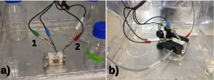
Figure 4 – Two electrode setup for electrochemical processes: a) Initial setup with front view
of the sample. The yellow V2O5 film is exposed to a circular area (0,883 cm2) of electrolyte.
The green wire (1) is connected to the working electrode (ITO) and the red (2) to the counter electrode (Pt wire), submersed in electrolyte; b) Complete setup for electro-optical measurements. The optical fibres are aligned with the circular areas where the thin film is exposed to electrolyte.
a
a
a
))
)
b
b
b
))
)
1
a
a
a
)
)
)
b
b
b
)
)
)
The typical procedure for testing the electrochromic properties of the V2O5 samples started with a CV, set at a scan rate of 25 mV/s with voltages ranging from -3 V to 3 V, for at least one cycle. This was done to prevent subsurface phenomena, the formation of a solid electrolyte interface, which interferes with the electrochromic properties of the material [53]. Following the CVs, several CA were carried out using a voltage sweep of -5 V to 5 V for 180 seconds.
Optical measurements were obtained simultaneously with the electrochemical experiments, using an OceanOptics USB4000 spectrometer in the 400 to 1000 nm wavelength range to obtain the transmittance through the electrochromic thin films. A custom-made ceramic cell was used to hold the sample in contact with the electrolyte, while allowing for optical measurements of the area in contact. These electrochemical experiments were performed using a liquid electrolyte solution of 0.5 M lithium perchlorate in propylene carbonate (LiClO4-PC). The solution was prepared by adding 5.32 g of LiClO4 to 100 mL of PC. The mixture was left on a magnetic stirrer at medium stirring rate for one hour.
2.5. Ion Beam Techniques
Ion beam techniques were used in this work to pre-lithiate and characterize the V2O5 thin films. These measurements were performed at the Accelerator and Radiation Technologies Laboratory (LATR) at CTN/IST (Lisbon, Portugal).
2.5.1. RBS and NRA
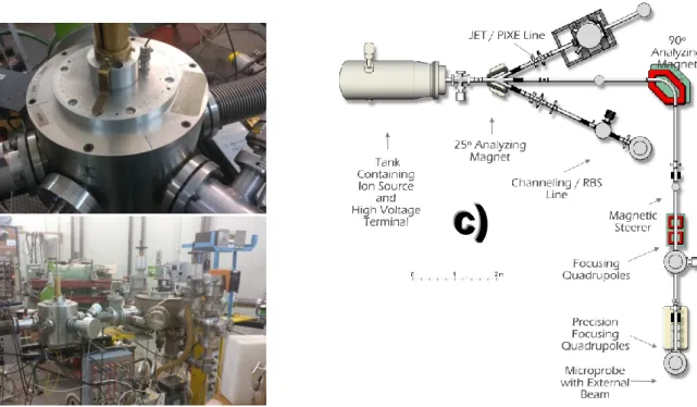
The stoichiometry and thickness of the targets were determined by means of RBS and NRA. These measurements were carried out at the 2.5 MV Van de Graaff accelerator of the LATR at CTN/IST. Three RBS detectors are placed symmetrically, two at 165° with respect to the beam direction (D1 and D3) and one at 140° (D2). The data analysis of the RBS spectra was performed with the NDF code.
Figure 5 – a) RBS chamber with three detectors and the sample holder inserted, b) RBS line setup and c) Diagram of the Van de Graaf Accelerator.
c
c
c)
)
)
b
b
b
)
)
)
a)
The beam enters the RBS/Channeling beam line after passing through a 25° analyzing magnet and through a pair of slits. The energy calibration of the accelerator is done using the calibration of this magnet. Three silicon detectors can be located in the chamber, where the scattered particles are detected. These are placed at θ = -140° (RBS2), θ = -165° (RBS1) and θ = +165° (ERD) with respect to the beam axis (figure 2 c). The lower scattering angle is used to avoid scattering particles from the chamber in the spectrum [55].
2.5.2. Ion Implantation
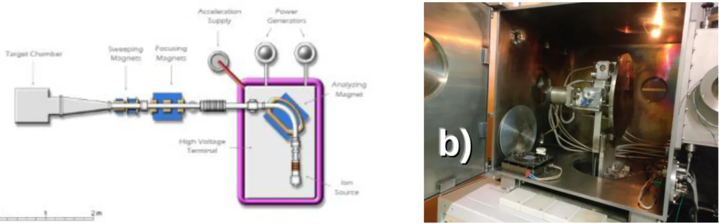
The implantation of 7Li was done at the Danfysik 1090 High Current Implanter at LATR/CTN. The source of ions is the model 921A High Current Source Ion (Chordis). The maximum acceleration voltage is 210 kV (50 kV at the extraction and 160 kV at the throttle tube) with currents up to 10 mA, target temperature between -150 and 600 °C, implanted area up to 40x40 cm2 and magnetic beam focusing and sweeping. Lithium-7 ions were implanted to a fluence of 1x10¹⁶ at/cm2, with implantation energy of 100 keV in three V2O5/ITO samples.
Figure 6 – a) Scheme of the Danfysic Ion Implanter at LATR/CTN and b) photograph of the target chamber. The samples are attached to the round metal support.
The analyzing magnet consists of a 90° double magnet with a mass resolution 𝑚/∆𝑚 from 150 to 250. The ion beam is focused by the focusing magnets, which are a triplet of magnetic quadrupoles. The samples are placed in the implantation chamber and mounted on a large metal target support with two rotating axes [55].
3. Results and Discussion
3.1. Crystallisation of V2O5 Thin Films: A Structural Characterisation
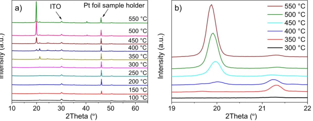
VOx thin films were produced using EBPVD deposited on ITO coated glasses. Due to the evaporation mechanism, the films are amorphous in the as-deposited state. In order to produce V2O5 thin films, the samples were annealed in air at different temperatures. Since V2O5 has one of the more stable stoichiometry of vanadium oxides, the annealing in an oxidizing atmosphere (air) promotes the crystallisation to orthorhombic V2O5. To characterize the temperature at which V2O5 is formed a sample was analysed in the heating chamber of the XRD system to allow the in-situ characterisation and tune the crystallisation behaviour of vanadium oxide. In this configuration, the sample is positioned in a platinum foil that is heated while performing the XRD scans.
Figure 7 – In-situ XRD analysis of VOx films: a) XRD scans at different filament temperatures
and b) a close-up of the same XRD analysis in the 19º - 22º 2Theta range for the high-end temperatures
These in-situ preliminary tests were performed to visualize the crystallisation of the VOx structure, as well as to verify the annealing temperature ranges where the newly obtained V2O5 structure was visible using XRD. An intense peak at position 2Theta = 46.2º is consistent throughout every scan and represents the Pt foil sample holder in the XRD system. Below 300 ºC, the films are amorphous and only ITO related peaks at 30.1º are visible in the diffractograms. At 350 ºC a new phase is present, as seen by the reflection at 2Theta = 21.3 º that disappears at 450 º C. For temperatures above 450 ºC the detected peaks can all be matched to orthorhombic V2O5 phase. Figure 6 a) shows the formation of a peak around the position 2Theta = 19.8º at 450 ºC which then increases in intensity for subsequent annealing temperatures. Figure 6 b) emphasizes this diffraction peak to show the increase in intensity.
For ensuing annealing studies, samples of layered glass, ITO and VOx were annealed in a muffle furnace at different temperatures to ensure the crystallisation of the films as V2O5. A temperature range of 350 ºC to 500 ºC was considered for following annealing studies to observe the effect of temperature on the structure of the VOx samples to draw further conclusions regarding the crystallisation. In figure 7 the XRD pattern obtained from a sample submitted to a thermal treatment of 1 hour at 450 ºC in the furnace is presented.
10 20 30 40 50 60 ITO 550 °C 500 °C 400 °C 450 °C 300 °C 250 °C 200 °C 150 °C 100 °C 350 °C Intens ity (a .u.) 2Theta (º)
a) Pt foil sample holder
19 20 21 22 550 °C 500 °C 450 °C 400 °C 350 °C 300 °C Intensi ty (a .u.) 2Theta (º) b)
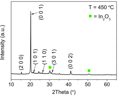
10 20 30 40 50 60 (3 0 1) (1 1 0) (0 0 2) (2 0 0 ) (1 0 1) T = 450 ºC In te ns ity (a .u .) 2Theta (º) (0 0 1) = In2O3
Figure 8 – XRD scan of annealed sample in the furnace at 450 ºC
The results shown are similar to those shown in figure 7, which were obtained in the heating chamber of the XRD system. The diffraction peaks correspond to an orthorhombic V2O5 phase (a = 11.516 Å, b = 3.5656 Å and c = 4.3727 Å; PDF 00-041-1426) and were assigned to the planes: (2 0 0) at 2Theta = 15.4º, (0 0 1) at 20.2º, (1 0 1) at 21.7º, (1 1 0) at 26.2º, (3 0 1) at 31.1º and (0 0 2) at 41.1º. These values are consistent with reported V2O5 depositions on ITO using EBPVD [56,57]. There are additional diffraction peaks at 2Theta of 30.2º and 50.6º that correspond to the (2 2 2) and (4 4 0) planes of ITO layer (In2O3; PDF 00-006-0416) beneath the V2O5 film, respectively.
A XRD scan was also performed on a sample submitted to an annealing at 500 ºC as a means of comparing the effect of furnace annealing on the structure of the orthorhombic V2O5 thin films. This comparison showed no significant difference between the two samples. Since the substrates used in this project are glass coated with ITO, a maximum temperature of 450 ºC (for 1 hour) was chosen to produce the V2O5 thin films used to study the lithium intercalation.
3.2. Lithium Intercalation by Electrochemical Processes
3.2.1. Optical Characterisation of V2O5 Films
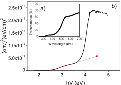
After the annealing the thin films changed from a dark grey colour to yellow, typical of V2O5 films. An optical characterisation was performed in order to extract the band gap of these films, presented in figure 8.
Figure 8 a) represents a typical transmittance spectrum obtained for the post-annealed V2O5 samples throughout this investigation. The %T increases the most at wavelengths from 430 nm to 550 nm, from 8.3% to 60.7% (ΔT% = 52.4%), which suggests this is the region of the material’s optical band gap, where a carrier transition occurs. It represents the threshold where photons with sufficiently low wavelengths have enough energy to be absorbed in the thin film. [58] The spectrum follows a similar tendency to that obtained by other authors using annealed V2O5 thin films [56]. The optical band gap is determined in graph b) by plotting Tauc’s law:
𝛼 ℎ 𝑣 = 𝐴 (ℎ 𝑣 − 𝐸𝑔) 𝑛
2 3 4 5 0 5.0x10¹¹ 1.0x10¹² 1.5x10¹² 2.0x10¹² 2.5x10¹² 300 400 500 600 700 0 20 40 60 80 100
(
h )
2(eV/
cm
)
2hV (eV)
a)
T rans m itt anc e (%) Wavelength (nm)b)
Figure 9 - Optical characterisation of V2O5 and ITO thin films: a) Transmittance spectrum of in
the 250 nm to 700 nm wavelength interval (UV-VIS region) and b) the corresponding Tauc plot used for extrapolating the optical band gap
Where 𝛼 is the absorption coefficient (cm-1); ℎ 𝑣 is the photon energy (eV); 𝐸
𝑔 is the optical band
gap (eV); 𝐴 is an intrinsic energy constant of the material and n which depends on the transition. The exponent, 𝑛, can assume the value of 2, 3, 1/2 or 3/2 for indirect allowed, indirect forbidden, direct allowed and direct forbidden transitions, respectively [7]. For V2O5 thin films, particularly those deposited by EBPVD, Ramana, C. V. e Hussain, O. M. reported that a direct forbidden transition with 𝑛 = 3/2, resulted in the closest fitting to Tauc’s law in order to determine the optical band gap [59]. Krishnakumar, S., e Menon, C. S. justify this fitting on the idea that “the coordination number of the vanadium ion in the vanadate glass is the same as that in crystalline V2O5.” Thus, this similarity suggests that similar transitions take place in both crystalline and amorphous V2O5.
For these samples, a direct allowed transition (n = 1/2) was considered using the first slope of figure 8 a). Vanadium oxides of different oxidation states present distinct electronic transitions [60], which can be verified by the two distinct slopes from the Tauc plot. An Eg = 2.48 eV was determined for the V2O5 Tauc plot. The optical band gap in literature for a direct allowed transition is reported as 2.58 eV for V2O5 thin films deposited by EBPVD at 400ºC [34]. The experimental values are in good agreement with literature, an experimental error of 3.9% was obtained.
3.2.2. Electrochemical Characterisation of V2O5 Films
In the electrochemical characterisation of the V2O5 thin films, samples were subjected to cyclic voltammetry scans (CV) as a way to verify the occurrence of oxidation-reduction reactions. In order to choose a setup for redox reactions to occur, different variables were tested: the scan rate and voltage range. The procedure consisted of two electrodes, using a Pt wire as the counter electrode. These experiments were performed on films analogous to those reported in the previous chapter and are presented in figure 9. Different scan rates and voltage ranges were tested to optimize the
measurements.
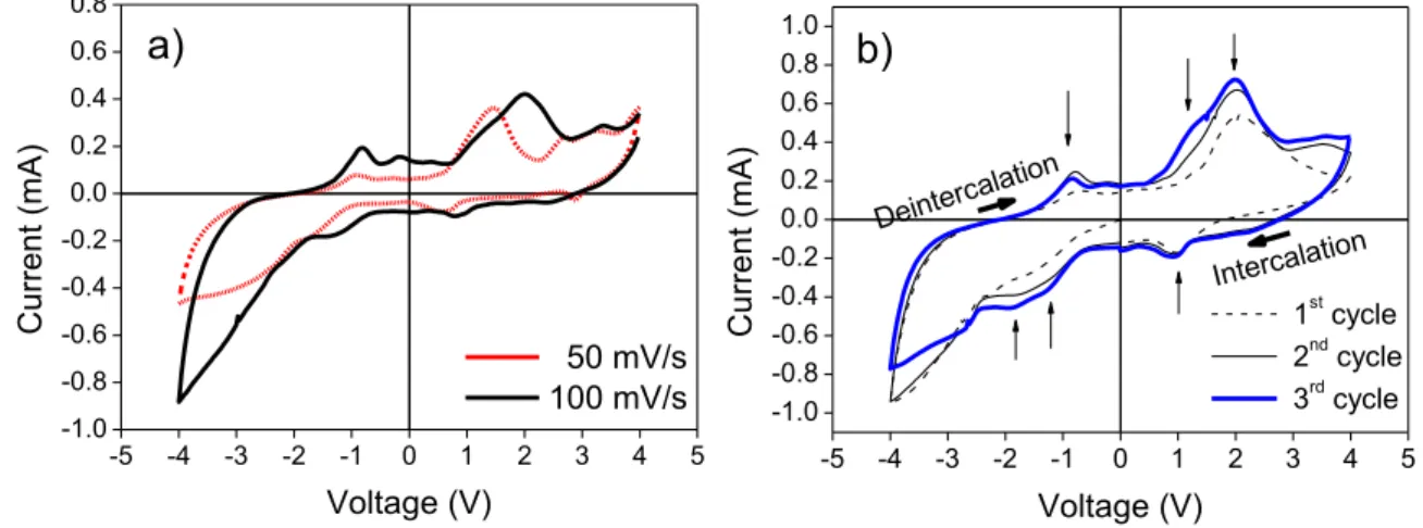
Figure 10 – a) Cyclic voltammograms showing the effect of scan rate on the redox reactions
of V2O5 thin films ; b) Cyclic voltammogram of a V2O5 film at a scan rate of 100 mV/s. The
arrows denote the scan direction.
Figure 9 a) shows the effect of the scan rate on the voltammogram of the thin film. The higher scan rate resulted in more defined symmetrical peaks at -1 and 1V, as well as higher currents when 2 V were applied. In figure 9 b), three cycles are presented and there are three peaks denoted by arrows in both upwards and downwards swept voltages. The symmetry indicates the reversibility of lithium intercalation and deintercalation in the negative and positive voltages, respectively. The positions of the peaks on this voltammogram are found at larger voltages than the ones found in literature (between -1 to 1 V for other V2O5 thin films deposited on conductive layers) [61]. Several factors influence the effective voltage range: the electrode configuration being used, the thin film thickness and type of deposition used to make the film.
The negative sweep from 0 V to -4 V leads to lithium intercalation, as the voltage goes to positive values the de-intercalation occurs. The most intense current peak at 2.1 V represents the majority of the oxidation reaction occuring in the film. The symmetrical peaks located near 1 V and -1 V, with respect to the origin, are also related to the oxidation/reduction of V2O5. For the majority of the analysed samples, the most intense peaks near ±2 V were present while the others were not always clear. Different voltage sweeps were tested from ±1 V to ±5 V, the peak near 2 V was always the more prominent so the voltage sweeps were kept between ±4 V and the scan rate at 100 mV/s. Published works also refer the presence of two-step electrochromism from yellow to green and green to blue [62], as can be verified in figure 9 b) due to the presence of several current peaks. The voltage ranges used in the electrochemical measurements throughout this work varied for each set of samples and had to be adjusted accordingly.
-5 -4 -3 -2 -1 0 1 2 3 4 5 -1.0 -0.8 -0.6 -0.4 -0.2 0.0 0.2 0.4 0.6 0.8 Cu rr e n t (m A ) Voltage (V) 50 mV/s 100 mV/s
a)
-5 -4 -3 -2 -1 0 1 2 3 4 5 -1.0 -0.8 -0.6 -0.4 -0.2 0.0 0.2 0.4 0.6 0.8 1.0 Deinterca lation 1st cycle 2nd cycle 3rd cycle Cu rr e n t (m A ) Voltage (V) Intercalationb)
3.2.3. Electro-optical Characterisation
The main objective of this study was to interpret and quantify the optical changes that occurred to the electrochromic V2O5 thin films, simultaneously while submitting the samples to cyclic voltammetry and chronoamperometry. The optical transmittance of the samples was measured in-situ with the electrochemical tests.
Li+ ion intercalation was conducted in a LiClO4-PC electrolyte solution using samples with an average thickness of 140 nm. The spectrophotometer was used to assess the optical characteristics of the films. Initially, the sample was intercalated with Li+ (“coloured”) by applying a chronoamperometric signal of -3 V for 180 s and then deintercalated (“bleached”) by applying the reverse procedure; +3 V for another 180 s. The optical transmittance spectra were obtained after each measurement and are presented in the figure 10.
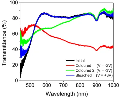
500 600 700 800 900 1000 0 20 40 60 80 100
Transm
itt
ance
(%
)
Wavelength (nm)
Initial Coloured (V = -2V) Coloured 2 (V = -3V) Bleached (V = +3V)Figure 11 - V2O5 optical transmittance in the UV-Vis-NIR spectral regions
From the initial to coloured state (at -2 V), there was a significant drop in transmittance with a 24.6% difference (85.5% to 60.9%) in the 600 nm wavelength. Qualitatively, the tested area of the V2O5 film changed from a dark yellow colour to cyan blue. When the sample was further biased with -3 V, a different transmittance curve (named “coloured 2”) was obtained, compared to the previous coloured state. This curve shifted to 67.0% transmittance at λ = 600 nm, while showing recovery to the initial state in the infrared region, from λ = 815 nm onwards. The initial and bleached optical states are identical which indicates the V2O5 recovered to its original oxidation state of V5+ as well as electrochromic reversibility for the first cycles. There are variations in the transmission spectra for different intercalation voltages, indicating different colours being produced by the intercalation of Li+ ions. These changes have been reported in other papers [8].
CV scans were then performed while recording the transmittance at fixed wavelengths (λ1 = 440 nm, λ2 = 510 nm, λ3 = 550 nm and λ4 = 650 nm) shortly before the conclusion of each individual electrochemical step. The graphs in figure 11 present the results of a sample submitted to five consecutive CV cycles.
Figure 12 - a) Optical transmittance for wavelengths λ1, λ2, λ3 and λ4 over five CV cycles. The
letters c and b denote coloured and bleached, respectively. ; b) The corresponding CV cycles of
the V2O5 film at a scan rate of 100 mV/s and ±3 V voltage range. The arrows denote the scan
direction.
As can be observed on figure 11 a), there is an abrupt change in the transmittance at all measured wavelengths when the voltage reaches -1.5 V, corresponding to Li+ intercalation. This step is maintained until the voltage reaches positive values, near +1 V. From the matching CV data (shown in figure 11 b) the electrochemical behaviour also indicates the main oxidation/reduction peaks near ±2 V indicating the correlation between the Li+ mobility in the thin film and the optical measurements. The consecutive CVs are similar indicating, that the process is reversible.
For these sets of samples, the peak at 2 V is more prominent and the pattern is similar to the one presented on figure 10, although not all peaks are visible. Repeated chronoamperometry scans were performed between the ±2 V voltage ranges for steps of 180 s. The same wavelengths were used to measure transmittance over time.
0
300
600
900 1200 1500 1800
0
20
40
60
80
100
T
ransm
ittanc
e (%)
Time (s)
= 440 nm = 510 nm = 550 nm = 650 nm c b-2
0
2
Volt
age (V)
VoltageFigure 13 – Optical transmittance for wavelengths λ1, λ2, λ3 and λ4 over five repeating
chronoamperometry scans. The letters c and b denote coloured and bleached, respectively.
From the graph in figure 12, it is possible to obtain the electrochromic parameters by finding the time required to reach the coloured and bleached state (tc and tb, respectively). These parameters are presented in Table 1.
0 25 50 75 100 40 60 80 100 40 60 80 100 0 400 800 1200 1600 2000 2400 40 60 80 100 -4 -3 -2 -1 0 1 2 3 4 -0.6 -0.4 -0.2 0.0 0.2 0.4 0.6 1 = 440 nm -3 0 3 V o lta g e (V) b c 2 = 510 nm 3 = 550 nm c 4 = 650 nm Time (s) b
a)
Transmi ttan ce (%) 1st Cycle 2nd Cycle 3rd Cycle 4th Cycle 5th Cycle Cu rren t (mA) Voltage (V)b)
Table 1 - Electrochromic parameters obtained from chronoamperometric measurements. The
parameters obtained for λ3 = 550 nm are highlighted.
λ (nm) Tc (%) Tb (%) tc (s) tb (s) ΔOD (λ) CE (cm2/C) Q (mC)
550 67.00 81.00 41 20 0.08 5.06
16.3
650 54.20 79.90 27 81 0.17 10.30
The coloured and bleached transmittance (wavelength dependent), Tc and Tb respectively, are found as the furthest points in each step before the voltage is inverted. The corresponding colouration and bleaching times (tc and tb) are found as the time taken for the transmittance to go from Tb–10%ΔT to Tc+10%ΔT and vice versa for tb. The variation in optical density, ΔOD, is given by:
𝛥𝑂𝐷 (𝜆) = 𝑙𝑜𝑔 (𝑇𝑏(𝜆) 𝑇𝑐(𝜆)
) 3
With the ΔOD calculated from equation 2, the colouration efficiency (CE) of the EC material is given as the variation in optical density per unit of inserted charge:
𝐶𝐸 (𝜆) = 𝛥𝑂𝐷 (𝜆)
𝑄 4
The accumulated charge is obtained by finding the integral of the current measured at each voltage step. Since V2O5 goes through many coloured states and the bleached state is not transparent (unlike other electrochromic materials) the optical density and the coloration efficiency were emphasized for the 550 nm wavelength as that is the standard for characterising electrochromic devices. A ΔOD = 0.08 and CE = 4.66 cm2/C were obtained ( = 550 nm). A CE = 22.8 cm2/C has been reported for V2O5 thin films prepared by sol-gel, annealed at 450 ºC and %T measured at = 600 nm [63]. The difference is a considerable 79.6%, however the preparation procedures for the thin films were widely different. There are few reports on the CE of V2O5, as this material doesn’t have a clear transmittance modulation like the one observed in WO3 [9], where the initial state is transparent.
3.2.4. Combined Structural and Electro-optical Measurements
A set of experiments were carried out to understand the effect of electrochemical intercalation on the structural properties of the material. A sample was measured at the XRD to verify the V2O5 peak’s positions and the crystallinity of the film prior to any test. Lithium was then inserted electrochemically by applying a negative bias through the ITO and measured again ex-situ on the XRD. A similar procedure was performed to deintercalate the Li ions. The XRD scans are presented on figure 13.
17 18 19 20 21
Int
ensi
ty
(a.u.
)
2Theta (º)
Initial -4.0 V +4.5 V +5.0 VFigure 14 – XRD scans of a V2O5 sample after each applied voltage in the 2Theta = [16.5,21]º
range
The sample was initially intercalated (-4.0 V) the main peak on V2O5 disappears and new small peaks near 16.7º, 18º, and 18.9º appear indicating the formation of a possible lithium vanadate. When applying the reverse voltage, the diffraction peak near 2Theta = 19.8º appears and then by forcing a more positive voltage (+5 V) the peak returns to the initial position of the (100) V2O5 plane. The position of the peak may indicate the presence of Li+ ions inside the lattice, and after +4.5 V the lithium was not totally extracted from the film. The intensity decreases indicating loss of crystallinity due to the Li+ ion movement. This behaviour was already reported by other authors [64]. Since these scans were performed ex-situ, the sample had to be dried off after each electrochemical experiment to remove liquid electrolyte from the thin film. This procedure is not ideal as it can harm the thin film surface, affecting the thin film’s ability to intercalate the Li+ ions.
To verify and characterize the structural response to the intercalation of Li+ ions, it was fundamental that the initial V2O5 was as similar as possible for each measurement. A sample composed of six different ITO electrodes, under the same V2O5 thin film, was tested electrochemically and each electrode was intercalated at different voltages. This sample was analysed by XRD and the results are presented in figure 14. As it can be seen, the most intense diffraction peak located at 2Theta = 19.8º goes through a shift to lower angles as the voltage applied to the electrode is decreased (to further negative values), being possible to conclude that the Li+ ions are being intercalated in the structure of V2O5. This suggests that the ion quantity is correlated with the peak position, resulting in an expansion of the crystalline structure along the c-axis.
The graph in figure 14 b) represents the relationship between the applied voltage (that induces intercalation) and the corresponding interplanar distance calculated for the crystallographic c-axis. These values are extracted from the respective XRD scans obtained in graph a) and using Bragg’s law:
Figure 15 – Ex-situ XRD scans of a six-electrode configuration sample: a) XRD scans in the 2Theta 18 to 21.5º range and b) the corresponding interplanar distance (crystallographic c
parameter) of the V2O5 in each electrode. The red markers indicate the values obtained for
non-intercalated V2O5.
Where d is the interplanar distance, θ is the incident angle of the ray, λ is the wavelength of the x-ray and n represents the order of diffraction. For these measurements, n = 1 is considered as the first order of the reflection planes is the most prominent. A photograph of the sample is also presented where it is possible to qualitatively observe the yellow colour of the V2O5 thin film (initial state), as well as the change from green to progressively darker blues, from the electrode with an applied voltage of -0.5 V (from the left) to the electrode submitted to -3 V (furthest to the right). The greatest shift in 2Theta (20.3º to 19.8º) and interplanar distance (0.008 nm difference) was observed from the initial state to -0.5 V. From these results it was concluded that the potential applied on the electrodes resulted in a shift of the highest intensity diffraction peak, which can be correlated with the lithiation in the films. A similar trend was observed in isolated samples (with different applied potentials) as a confirmation experiment for the structural characterisation.
3.2.5. Quantification of Li+ Ions by RBS and NRA Techniques
After the characterisation of the thin film given in the previous chapter, a series of experiments were conducted at CTN/IST to detect the presence of Li+ ions in this same sample. RBS and NRA measurements were performed in a Van de Graaff accelerator where an H+ beam with 2.0 MeV of energy was directed to the sample.
The protons from the beam can undergo an elastic collision with the samples’ surface and are backscattered with different energies, which depend on the kinematic factor of the collision given between the two interacting atoms. Some of these backscattered particles are detected by a particle detector, placed at an angle of 165º for this setup. This elastic collision analysis is referred to as RBS analysis. Nuclear reactions can also occur between the incident proton and lithium atoms (7Li and 6Li) present in the samples. In the case of 7Li, two high energy alpha (4He) particles can be produced. For this particular proton-lithium nuclear reaction, the emitted alpha particle is scattered with energy of 7.54 MeV and is also detected by the same particle detector. This analysis involving nuclear reactions is referred to as NRA.
RBS and NRA spectra were obtained for each electrode of the previously mentioned six electrode sample, where each electrode was electrochemically biased with a different voltage. The spectrum for the electrode subjected to –3 V is presented in figure 15 a) and b), where it is possible to observe the presence of the elements in the analysed sample.
18.0 18.5 19.0 19.5 20.0 20.5 21.0 21.5 0.0 -0.5 -1.0 -1.5 -2.0 -2.5 -3.0 0.440 0.444 0.448 0.452 0.456 0.460 0.464 -0.5V -1.0V -1.5V -2.0V -2.5V -3.0V Int ensi ty (a.u. ) 2Theta (°)
a)
b)
Int erplanar di st . c-axis (nm) Voltage (V)The energies of the particles backscattered by elastic collisions depend both upon the mass of atoms from which they scatter (kinematic factor) as well as the depth at which a collision occurs (energy loss factor). Energy barriers are present, which reveal elastic collisions beyond the samples’ surface. The width of these barriers gives a measure of the depth at which the collisions occurred. In figure 15 b), at energies above 7 MeV, a peak is observed which corresponds to the alpha particles produced by the nuclear reaction with 7Li atoms. This peak is an evidence of the interaction with Li atoms, and the area of the peak can be directly correlated with the quantity of 7Li in the sample. The energy dispersion (given by the peak width) is associated with the depth distribution of the intercalated Li atoms in the sample.
Analysis with fitting software was performed to extract the film’s composition that best describes the spectra. From these fits, it was possible to find the film’s stoichiometry and the Li content in each electrode. The fitting of the data obtained from the RBS and NRA measurements, shown in figures 15 a) and b), were performed using the NDF software [54]. A bulk density of 3.357 g/cm3 [65] was assumed for the V2O5 thin film.
The depth profile in figure 15 c) graphically illustrates the atomic percentages of the present elements in the samples, determined from the individual fit on the RBS spectra of each electrode. These Li depth profiles suggest that lithium ions diffuse further inside the sample towards the ITO layer and glass substrate. A bias of -1 V was enough for the Li+ ions to reach a depth of up to 391 nm (well inside the glass substrate), followed by a decrease to 363 and 279 nm at -2.5 V and -3 V, respectively. The total Li in the sample and V2O5 thin film was calculated considering the average percentage natural abundance of the two occurring isotopes on Earth, Li-6 and Li-7, with 7.42% and 92.58% respectively [66]. The Li quantities detected in the six-electrode sample are summarised in Table 2. 0 100 200 300 400 500 2 4 0 2 4
Depth (nm)
-0.5 VV2O5 ITO Glass substrate
-1.0 V -1.5 V 7
Li
count
(%
at
.)
-2.0 V -2.5 V -3.0 Vc)
800 1000 1200 1400 1600 1800 2000 2200 2400 0 10000 20000 30000 40000 Na Si O Ca V Li In,Sn Data 7Li 6Li V O Na Si Ca In Sn Fit Y iel d (Counts) E (keV)a)
Figure 16 – a) RBS spectrum of the
electrode biased with -3 V, showing the more abundant elements present in the sample, b) NRA spectrum of the measured electrode and c) graphic representation of
7Li atomic percentage as a function of
depth obtained by fitting the spectra.
1000 2000 3000 7000 7250 7500 7750 1 10 100 1000 10000 In,Sn 7 Li(p,)4 He Data Fit Y iel d (Counts) E (keV)
b)
Table 2 – 7Li and total Li quantities and C-axis interplanar distance for the respective voltages,
detected by RBS and NRA in the six-electrode sample.
Electrode Voltage (V) 7Li quantity (1015 at/cm2) Total Li quantity (1015 at/cm2) C-axis Interplanar distance (Å) E1 -0.5 22.20 23.94 4.486 E2 -1.0 44.00 47.44 4.495 E3 -1.5 50.93 54.91 4.508 E4 -2.0 51.50 55.53 4.552 E5 -2.5 58.80 63.40 4.591 E6 -3.0 56.40 60.81 4.627
From the values obtained in Table 2, it can be seen that the Li quantity increases with more negative voltages. This is expected, as more negative potentials resulted in higher currents (as seen from the CV data in chapter 3.2.2.) which attract more Li+ ions from the electrolyte solution to the cathode. Only electrode “E5” doesn’t follow this tendency, as it had a higher quantity of Li than electrode “E6”. However, from the depth profile in figure 15 c), it can be observed qualitatively that E6 has the most 7Li within the depth corresponding to the V2O5 thin film. This suggests that the more negative potentials are more effective at attracting Li+ ions towards the thin film itself for intercalation. Since the reduction peak seen during CV starts at -1 V and continues through to -3 V, the resulting current can be correlated with an increased intercalation of Li+ ions, which induces the redox reaction where LixV2O5 is obtained.
The interplanar distances along the C-axis are shown in the last column as it can be related to the Li quantification. The increased Li+ intercalation resulted in a greater phase of LixV2O5 that can contribute to the lattice expansion, when compared to the x-ray diffractograms obtained for regular V2O5. It is suspected that the quantities of Li detected within higher depths are associated with Li diffusion into the glass substrate.
3.3. Ion Implantation of Lithium
One of the main objectives was to investigate the effect of sample lithiation by ion implantation on the structural, optical and electrochemical properties of the V2O5 samples. An attempt was also made to quantify the presence and quantity of Li+ ions in the samples’ layers by RBS. A simulation was performed in the MonteCarlo SRIM program, assuming a 200 nm thick film of V2O5 deposited on a 300 nm In2O3 film, to guarantee that the implantation distribution peak was on the V2O5 layer. For the 7Li+ ion implantation, energy of 20 keV and a fluence of 1x10¹⁶ at/cm2 were used to introduce lithium ions in the samples.
The theoretical Li+ profiles for three different fluencies are presented in figure 16 a), obtained with the SRIM software. For this study, four samples were considered: two samples already annealed at 450 ºC i.e. crystalline V2O5 and two amorphous samples (VOx). The ion implantation was performed in two samples; one with crystalline V2O5 (annealed) and another in the amorphous phase. For clarity, these were named as c-V2O5(Li) and a-VOx(Li), respectively.
The latter sample was then annealed after the implantation. This method was used to verify the effect of the thermal treatment on 7Li+ ion intercalation. Non-implanted VOx (a-VOx) and crystalline V2O5 (c-V2O5) samples were considered for comparison. All four samples in this chapter had approximately the same thickness of 300 nm.
![Figure 2 – a) Representation of a two electrode setup. The arrows indicate the direction of charge carrier flow during intercalation in to the electrochromic material, deposited on the WE [42]; b) Cyclic voltammogram obtained from ap](https://thumb-eu.123doks.com/thumbv2/123dok_br/15244922.1023492/15.892.92.778.454.737/representation-electrode-indicate-direction-intercalation-electrochromic-deposited-voltammogram.webp)