Nb-doped Ti
2O
3Films Deposited Through Grid-Assisted Magnetron Sputtering on Glass
Substrate: Electrical and Optical Analysis
Joel Stryhalskia,b* , Diego Alexandre Duartec , Luis Manuel Reboutad, Julio César Sagása,
Carlos José Tavaresd, Luis Cesar Fontanaa
Received: July 26, 2018; Revised: December 20, 2018; Accepted: January 07, 2019
Niobium doped dititanium trioxide (Ti2O3:Nb) films were deposited on glass substrates, through
grid-assisted magnetron sputtering. The Ti2O3:Nb films were characterized by X-ray diffraction
(XRD), electrical conductivity and optical properties. Film deposition was carried out in two different substrate bias modes: DC and unipolar pulsed. Results show that the negative-pulsed mode improves conductivity and crystallinity. The XRD results show peaks corresponding crystallographic planes of
Ti2O3. No niobium oxide NbxOy peaks were observed, which indicates that niobium oxide if formed,
is amorphous, and/or substituted Nb atoms remain in a solid solution within the Ti2O3 structure. It was observed that "as-deposited" Ti2O3:Nb films (without post annealing) are transparent and electrical
conductive, with transmittance that reaches 60% in the visible light wavelength despite the considerable thickness of the film and a miminum resistivity of 2x10⁻² Ω.cm which indicates that there is potential for application as Transparent Conductive Oxide (TCO).
Keywords: Dititanium trioxide Ti2O3, Niobium doping, electrical conductivity, substrate bias,
grid-assisted sputtering.
*e-mail: [email protected]
1. Introduction
Titanium oxides are semiconductor materials that have two main stoichiometries: TiO2 and Ti2O3. Titanium
dioxide TiO2 has been extensively investigated in the last
three decades due to its various technological applications in different areas such as catalysis, optical and electronic devices, biology 1,2,3.
Much research is focused on improving the harvesting of solar light and its conversion into other forms of energy or chemical reactivity. The strategy for this purpose can be done by doping TiO2 in order to reduce the band-gap energy
and to achieve absorption in the visible light region. In 2005, Furubayashi et al. 4 reported that Nb-doping
into TiO2 (anatase) produced transparent conducting oxide
(TCO) films. The resistivity of such films was as low as
10-4 Ω.cm at room temperature. Since then, many papers
have been published on this topic due to the interest in the application of this material in different devices, including flat panel displays (FPD), light-emitting devices (LED), solar cells and photo-induced activity 5,6,7. Given that,
TiO2:Nb has been investigated as an alternative material to
substitute ITO films due to the toxic nature of the indium. Titanium niobium oxide has been obtained through different
processes because niobium is substitutionally incorporated
in the TiO2 host at cationic lattice sites
8. The changes in the
electronic structure of TiO2 due to Nb doping have already
been discussed in the reported literature 9. Because of the
presence of the extra “d” electron, Nb should populate the metal “d” band, thus yielding an oxide metallic system 10.
The Nb donor gives a shallow state, forming Ti4+ and Nb5+
ions 11. The ionic radius of Nb5+ is slightly larger than that of
Ti4+ (r
(Ti4+)=0.605 Å versus r(Nb5+)=0.64 Å) and has dimensions
similar to Ti3+. Therefore, Nb5+ can be easily doped into the
lattices of TiO2 and Ti2O3 at high concentration 12.
In order to facilitate the doping of Nb5+ ions into the
TiO2 crystalline structure, in place of Ti4+, two mechanisms
have been proposed: 1) one Ti4+ cation vacancy is created
for every four Nb5+; and 2) reducing Ti4+ to Ti3+ for every
Nb5+ incorporated is also possible 13. The metastable anatase
phase of TiO2 (band gap of 3.2 eV) is of great interest for
Nb-doping, which, in optimized conditions, can achieve a resistivity on the order of 10-4 Ωcm. Nb-doped rutile TiO
2 is
resistive, and from photoemission experiments, it has been found that Nb introduces a deep state lying about 0.8 eV below the conduction band 9.
On the other hand, it was found that TiO2 should be slightly
oxygen-deficient or annealed in a reducing atmosphere, otherwise the donor (Nb) action may not be effective 8.
The problem is that the donors may be compensated by interstitial oxygen anions if the TiO2 anatase polymorph has
high oxygen content. Therefore, to avoid interstitial oxygen in the TiO2 structure, the films should be deposited with
aDepartamento de Física, Universidade Federal de Santa Catarina, Joinville, SC, Brasil
bDepartamento de Física, Instituto Federal de Santa Catarina, Jaraguá do Sul, SC, Brasil
cUniversidade Federal de Santa Catarina, Joinville, SC, Brasil
low oxygen partial pressures. When performing deposition through magnetron sputtering, the film should be deposited before the poisoning point threshold on the hysteresis curve of the cathode voltage versus pressure plot. In other words, the deposition of oxygen-deficient film should be carried out in metallic mode. Films deposited in oxygen-deficient conditions correspond to those at Ti2O3:TiO2 equilibrium,
and it can be expected a mixture of different titanium oxides
(TiO2 and Ti2O3), as reported by other authors 14,15
From the literature, the Ti2O3 oxygen-deficient phase has
gained less attention in comparison to stoichiometric TiO2.
However Ti2O3 features thermochromic and photocatalytic
properties, allows absorption of visible light, has relatively high electrical conductivity and is able to serve as a transparent
conductor (TCO) 16,17. This paper will study the optical and
electrical properties of niobium-doped dititanium trioxide
(Ti2O3:Nb) films. The Ti2O3:Nb system may improve the film's
electrical properties by considering two effects, namely: 1)
Ti2O3 may be considered as a sub-oxide of TiO2 and leads
to the donation of electrons in Ti 3d bands; and 2) the donor Nb should also populate the metal “d” band.
Moreover, crystalline Ti2O3 films are easier to obtain than TiO2, without recovering by annealing. It is a very important
point when films are deposited on a temperature-sensitive substrate, in which thermal annealing is not possible.
It is well known that film crystallinity may be improved through biasing the substrate during film deposition 6. It
increases the energy of the incoming ions, allowing the adatoms to migrate to more suitable sites. Pulsed bias is suitable for deposition of insulator films by reactive sputtering, thus avoiding the accumulation of static charge on the surface of the dielectric film during the deposition process 18, 19. Previous
studies have demonstrated improvement of the crystallinity of TixOy and TixNy films through the negative pulsed biasing
substrate 20. Thus, in an attempt to produce films with good
transmittance and low electrical resistivity, the effect of the Nb-doping and the pulsed bias on the electrical and optical properties of oxygen deficient Ti2O3 thin films, deposited by
grid assisted magnetron sputtering (GAMS), was investigated.
2. Experimental Procedure
Ti2O3:Nb films were deposited onto borosilicate glass
substrates (0.16×16×16 mm3) using GAMS. This system
differs from conventional magnetron sputtering due to a grounded grid that is strategically placed in front of the target (at approximately 2 cm from the cathode surface). Such an arrangement improves the plasma stability and allows for operating the system at slightly lower pressure. It shifts the first critical point in the hysteresis curve and allows for better control of the sputter process and film properties 21,20,22,23,24.
The sputtering target was composed of a Ti disc (99.5% purity, 100 mm diameter, 6.0 mm thickness) containing 12 Nb inserts (99.5% purity, 3.0 mm diameter), symmetrically
disposed in its erosion track, this target produces Nb/Ti ratio of 0.11 ± 0.02.
In the first step, the process parameters for optimized films with stoichiometry and crystalline structure closest to
Ti2O3, without recovering by annealing, were established.
These parameters are shown in Table 1. The process parameter chosen to be studied was the substrate bias, which could be selected on either “DC mode” or “pulsed mode”, within a voltage range of 0 V to -200V. The plasma was powered by a DC power supply, controlled in current and voltage up to 2.0 kV. In the current study, the film depositions were carried out with a target power density of 6.0 W/cm2.
A set of hysteresis experiments was carried out to determine the conditions for deposition of the sub oxide Ti2O3. Indeed,
from these experiments, the value of reactive gas flow closest to the metallic mode threshold on the hysteresis curve (known as the first critical point) was determined. Figure 1 shows the critical point on the hysteresis curve for the working pressure as a function of the oxygen flow rate. All depositions were made at this threshold of the metallic mode. Results show semi-transparent films with bluish color (shown in detail in Fig. 1), indicating the formation of oxygen-deficient TixOy.
Table 1. Process deposition parameters for deposition of Ti2O3:Nb films.
Parameter Value
Grid-target distance 2.0 cm
Target-substrate distance 6.0 cm
Ar (flow rate / partial pressure) 2.0 sccm / 0.1 Pa O2(flow rate / partial pressure) 3.5 sccm / 0.3 Pa
Target power density 6.0 W/cm2
Substrate temperature 400±10 °C
Vbias
-100V, -200 V DC DC -100V, -200V pulsed (1.0 kHz, 20% duty cycle)
Deposition time 30 minutes
Figure 1. Hysteresis curve of total pressure (Ar + O2) as a function
Preliminary tests showed that the most effective bias voltage range impacting on the microstructure and crystallinity of films was between -100V and -200V, in both DC and pulsed modes. DC bias voltage below ǀ-100Vǀ is not effective because the ion current drawn at the substrate is not sufficiently energetic; on the higher limit, a bias voltage above ǀ-200Vǀ produced excessive re-sputtering on the film surface. Other authors have found a significant increase in the ion current drawn at the substrate holder due to the pulsing substrate bias voltage in the mid-frequency range 100-350 kHz 14. However, within this frequency range,
the voltage “time off” is too short for cancelling the static positive charge accumulated at the insulator substrate (this neutralization should be done mainly by electrons flowing from the glow discharge).
Pulsed bias voltage were applied at the substrate holder, relative to the ground. During the negative pulse of voltage bias, the positive ions are attracted to the holder; subsequently, when the bias falls to zero volts, electrons and energetic negative ions (e. g. negative oxygen), coming from the plasma, can also impinge on the holder due the lower potential barrier. In this way, by pulsing the bias voltage, it is possible to neutralize the static charges on the surface of the insulator film. The surface of the insulator substrate is thereby bombarded by ions and electrons at every period. In the present case, the required period for efficient pulsed biasing (e. g. the time needed for the current to drop to zero Ampere) was approximately 1 ms. Learning from this, in pulsed mode, the film deposition was carried out with a bias frequency and duty cycle of 1.0 kHz and 20%, respectively. As it will be shown, this bias condition produces relevant changes in film crystallinity.
The deposited films were characterized by X-ray diffraction (Shimadzu XRD-6000), UV-Vis-NIR spectrophotometry (Shimadzu model UV-3101) and four-point probe electrical measurements using the van der Pauw method. The chemical composition of the films was obtained from energy dispersive X-ray fluorescence spectrometer (EDX) analysis using a Shimadzu EDX-720/800HS device. Results showed that Nb/Ti ratio was 0.11±0.02 for all films deposited.
Transmittance T and reflectance R measurements (between 250 nm and 1200 nm) allowed for the determination of the band-gap energy of the Ti2O3:Nb films through the Tauc Plot
method 25. The absorption coefficient α and film thickness d were fitted using the SCOUT software package 26 through
equation 127.
(1)
The refractive index (η) and extinction coefficient (κ) as a
function of the wavelength, as also the thickness of individual layers, can be obtained from the reflectance and transmittance measurements. This can be done because Reflectance (R), Transmittance (T) and Absorptance (calculated from T and
R) depend of the optical constants and thickness of those layers. Thus, fitting the data simultaneously with a specific model, the calculation of spectral optical constants, can be performed 28,29,30. The experimental transmittance and
reflectance curves were modelled using a commercial optical simulation program (SCOUT).
The model used in this software assumes that there are several types of oscillators, each one with their own characteristic resonant frequency, allowing calculation on the frequency dependence of the complex dielectric
constants
f
u
r=
f
u
Drude+
f
u
TL, which can be used to obtainoptical constants, such as refractive index (n) and extinction
coefficient (k). The Drude model
f
u
Drude describes theintra-band transitions of electrons in the conduction intra-band, while the Tauc-Lorentz
f
u
TL model is used for optical transitions forinter-band transitions from the valence band to the conduction band. More details about the model can be found in the
literature 31,32. Previously to the calculation of the optical
properties of the films, reflectance and transmittance of the glass substrate is modelled and its dielectric function is used in the remaining calculations. The electrical properties of the films (resistivity, electronic mobility and charge carrier concentration) were obtained through Hall effect measurements. The charge carrier concentration (nD) and
carrier mobility (µ) are given by 31:
(2)
(3)
where I is the electric current, B is the magnetic field (in Gauss), d is the film thickness, q is the elementary charge, Vs is the Hall voltage and Rs is the sheet resistance. These
measurements were carried out under dark conditions at room temperature, using a four-point probe in the van der Pauw configuration 33, with a magnetic field of 1.0 T, and
using a Keithley 2410 current meter.
3. Results and Discussions
Table 2 shows the bias current and film thickness for different values of bias voltage. Results indicate that the bias current was higher for pulsed voltage (at peak) than for DC bias. This is attributed to the exchange of static charge on the surface of the dielectric substrate; the surface of the insulator substrate is thereby bombarded by ions and electrons at every period increasing the current on the substrate. The effect of DC bias on the film thickness is negligible. On the other hand, in pulsed mode, a higher bias voltage (-200 V) produces thinner films when compared to a lower voltage (-100 V). It is well known that energetic ions accelerated in high voltage may produce re-sputtering of adatoms, thus decreasing the film thickness 19.
ln
d
R
T
1
a m
=
m
m
-Q
V
"
Q
Q
V
V
Q
V
%
Figure 2 shows the X-ray diffraction patterns for the
Ti2O3:Nb films providing substrate bias of -100 V and -200
V, in both DC and pulsed mode. For comparison, a diffraction pattern of a grown film with grounded substrate is also shown. The diffraction peaks located at 32.9º and 53.5º are associated with (104) and (116) reflections indexed to rhombohedral (R-3c) Ti2O3 (JCPDS card reference: 43-1033, 1997); the
broad peaks are related to the glass substrate.
Taking into account the information in Table 2, it is possible to correlate the intensity of XRD peaks with the bias current; that is, the film crystallinity increases as the bias current increases. The ion bombardment promotes the formation of oxygen vacancies and the bluish color can be due to some charge transfer forming Ti3+. TiO
2 reduction was
seen after neutron and electron 11 bombardment. The oxygen
vacancies associated with Ti3+ valence state originates an
in-gap state in the form of an intermediate band just below the conduction band of the host material. No diffraction peaks associated with niobium oxide were detected, despite the high concentration of Nb in the film (Nb/Ti ratio of 0.11 ± 0.02). Thermodynamic data suggest that the synthesis of
TixOy is more likely than NbxOy because the heat of formation
of the former is greater 34. In addition, as discussed in the
introduction, Ti4+ and Nb5+ have a very similar ionic radius,
and Ti3+ has higher radius, allowing for a large solid solution
of Nb in the titanium oxide structure. These diffraction peaks appear to be slightly shifted to lower angles (~0.2º), which can be due to the compressive biaxial residual stress usually induced by high substrate polarization. Additionally, this shift to lower angles can also be due to a lattice distortion caused by substitutional Nb atoms, taking into account the aforementioned difference in ionic radius of the metal ions. This data cannot exclude the formation of niobium oxide, which could be located in the grain boundaries.
Figure 3 shows the optical transmittance results of ensemble film/substrate. The highest average transmittance (~50%, between 400 nm and 600 nm) was achieved for
Ti2O3:Nb films grown providing bias of -200 V in pulsed
mode. However, in this condition, the films are thinner than the rest (see Table 2), and this is the main reason that it has the highest transmittance, as discussed below.
Figure 4 shows a standard optical property normalized regarding the film thickness, that is, the intrinsic absorption
coefficient α(λ). It was calculated from values of the
transmittance (T), reflectance spectra (R, not shown) and thickness (d) of the films obtained through the SCOUT software 26, as described in ref. 32. The complex refractive
index ñ is usually defined as equation 4.
(4)
(5)
The real part of ñ, namely n, is refrative index, and the imaginary part k is extinction coefficient. The extinction
Figure 2. X-ray diffraction patterns for Ti2O3:Nb films grown on glass with varying substrate bias voltage.
Table 2. Film thicknesses and bias current at the substrate as a
function of bias voltage (DC and pulsed DC modes) for Ti2O3:Nb reactive deposition.
Substrate bias
Film thickness (µm) Voltage (V) Current (mA)
-100 DC 5.0 0.26
-200 DC 6.0 0.27
-100 Pulsed 9.0 peak 0.26
-200 Pulsed 12.0 peak 0.16
Figure 3. UV-Vis-NIR transmittance response for Ti2O3:Nb films grown providing DC or pulsed bias to the substrate holder.
n
u
=
n
+
ik
k
4
a m
m
r
=
coefficient is directly related to the absorption coefficient
α(λ) of the medium as showed in equation 5.
Fig. 3 shows a wavy curve between 400 and 500 nm that suggests the presence of interference effects because the thickness of films and reflection of air-film and film-glass substrate. In most cases it is possible to ignore multiple reflections between the front and back surfaces 32 and, thus,
equation 1 can be used. It is useful when semiconductor laser diodes or optical bistabilities are studied. In many cases, the effects are small enough to be neglected as the results found in the literature 32,27,35. This is why tables of transparent optical materials properties generally list only the real parts 32,36.
The simulations obtained with Scout and with equation 1 are very similar in the spectrum range between 400 nm and 1200 nm , and α is about 35x105 m-1, without changing significantly for films obtained with different bias voltages. Therefore, different values of transmittance (as seen in Figure 3) can be attributed mainly to the change in thickness of the coatings. However, from 500 nm to about 1000 nm, an increase in the absorption coefficient is registered, as seen in Figure 4, which can be correlated with the presence of oxygen vacancies. This absorption band is attributed to Ti3+ -Ti4+
charge-transfer 37,38 and is also an additional confirmation
of the presence of titanium ions in the Ti3+ oxidation state.
Figure 5 shows the refractive index results as a function of wavelength for the produced Ti2O3:Nb films. The average
refractive index values shown are close to those reported in the literature (between 1.9 and 2.3 for Ti2O3
39, between
2.49 and 2.54 for anatase, and between 2.79 and 2.90 for rutile, for visible range) 40. According to studies conducted
elsewhere 40, the refractive index depends on properties
such as film density and homogeinity, lattice distortion (for example, due to dopants and impurities), degree of crystallinity and residual stress of the film. In this paper, films grown providing -100V pulsed as substrate bias feature a slightly higher refractive index than the rest.
The higher refractive index may be due to the increase in film density and improvement of crystallinity and overall homogeinity caused by moderate ion bombardment during film deposition, as well as due to the presence of a mixture of different titanium oxides. However, these hypotheses need further investigation.
Figure 6 shows the Ti2O3:Nb band-gap energy evolution
with applied substrate biasing, calculated through the Tauc method for indirect transitions 25,41. Results show a small increase of band gap energy from 3.26 ± 0.06 eV to 3.33 ± 0.06 eV for films deposited with voltage bias -100 V and -200 V in DC mode, respectively. An increase from 3.19 ± 0.06 eV to 3.35 ± 0.06 eV was also observed for films grown providing -100 V and -200V in pulsed mode respectively. The band gap energy values are lower than those presented in the literature for TiO2:Nb (3.68 eV)
42, but are close to
the values for pristine TiO2. Table 3 shows a comparison
between band gap values for: TiO2 8,40, TiO
2:Nb 9,42, Ti
2O3 43,
and Ti2O3:Nb (obtained in this work). In addition, the bluish
aspect is an evidence that a fraction of titanium ions exists in
Ti3+ valence state. Nakamura et al 44 proposed a band structure
model with oxygen vacancy state lying 0.75 eV below the conduction band. The ionization energy, i.e. band-gap energy between the oxygen vacancy states and conduction band, was calculated using the Tauc plot for direct transitions and is in the range of 0.57 to 0.69 eV in the present films, as shown in Figure 7; this is correlated with the number of oxygen vacancies created during film growth 44.
These results are in agreement with reported values in the literature, corresponding to localized states that lay between 0.6 and 1 eV below the conduction band 45. These states are considered important for photocatalytic oxidation processes, and could be responsible for the enhancement in the electrical properties, as shown later in this manuscript.
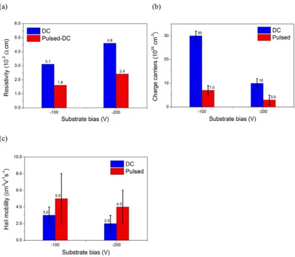
Figure 8 shows the results for electrical resistivity, charge carrier concentration (mainly electrons, as indicated by the Van der Pauw measurements) and electron mobility. An electrical resistivity of ~10-2 Ωcm for as-deposited Ti
2O3:Nb
films was observed. This value is at least five orders of
Figure 4. Intrinsic absorption coefficient as a function of wavelength
(obtained from Scout simulations) for Ti2O3:Nb films deposited with varying substrate bias.
magnitude lower than electrical resistivity of bulk Ti2O3,
as reported 46. The decrease in resistivity is attributed to
the presence of an extra “d” electron, from Nb, that should populate the conduction “d” band of Ti2O3:Nb, as discussed
above. Fig. 8a shows the resistivity slightly decreasing when the film is deposited with pulsed bias instead of DC bias. It may be related to the improvement in the film crystallinity and decreasing of defects, when the films are deposited with pulsed bias, since this leads to less charge scattering centers. For depositions with the same bias voltage, the observed results are quite interesting because while the charge carrier concentration (Fig. 8b) decreases, the mobility (Fig. 8c) increases. This happens when there is a change in substrate bias mode from DC to pulsed. Although the cause for the decrease in charge carrier is not clear, charge carrier
mobility may increase by reducing lattice defects that act as scattering centers. Therefore, increasing mobility (caused by higher crystallinity in pulsed mode) leads to a reduction of film resistivity, despite the results showing a decrease in charge carrier concentration.
4. Conclusions
When doped with Nb, the sub-oxide Ti2O3 films reveal
properties of a transparent conductor oxide (TCO), As-deposited
Ti2O3:Nb films on glass substrate through grid-assisted
magnetron sputtering showed electrical resistivity values on the order of 10-2 Ωcm. However, Ti
2O3:Nb resistivity values
are two orders of magnitude greater than those known for
TiO2:Nb with post annealing.
Regarding the optical properties, Ti2O3:Nb films show
optical transmittance between 30% and 50% for incident radiation between 400 nm and 700 nm, that is, in the visible optical range, this value is close to that achieved for ITO 47.
The estimated band gap energy is similar to that of pristine
anatase TiO2, of approximately 3.25 eV. The presence of
titanium ions in the Ti3+ oxidation state is in accordance with
the results obtained by XRD, with the identification of the
Ti2O3 phase, with an absorption band in the region 500-1200
nm, and by the gap state 0.6 eV below the conduction band Electrical property results revealed that DC pulsed substrate biasing decreases the resistivity for Ti2O3:Nb films.
Pulsed bias increases substrate current and improves film
Figure 6. Tauc plots (for indirect transitions) corresponding to Ti2O3:Nb films grown providing -100V and -200V substrate bias in both DC and pulsed modes.
Table 3. Band gap comparison between TiO2, TiO2:Nb, Ti2O3, and Ti2O3:Nb
Oxides Band gap References Transition
TiO2rutile ~ 3.0 eV 9 Direct
TiO2anatase ~ 3.2 eV
8,27,40 Indirect
TiO2:Nb 3.68 42 Direct
Ti2O3 3.81 eV 43 Indirect
Ti2O3:Nb
3.70 to 3.82
eV This work Direct
Ti2O3:Nb
3.19 to 3.35
Figure 7. Tauc plots for direct transitions from the Ti3+ valence state of Ti
2O3:Nb films grown providing -100V and -200V substrate bias in both DC and pulsed modes.
crystallinity and homogeneity, which tends to reduce charge scattering centers and, thus, the electrical resistivity. This GAMS deposition technique was shown to be promising for obtaining low resistivity and high transparency thin films, dispensing with a subsequent heat treatment; hence, more interesting for large-scale production.
5. Acknowledgments
This study was supported by the Government of the State of Santa Catarina through the FUMDES and FAPESC programs.
6. References
1. Diebold U. The Surface Science of Titanium Dioxide. Surface Science Reports. 2003;48(5-8):53-229.
2. Gonçalves P, Bertholdo R, Dias JA, Maestrelli SC, Giraldi TR. Evaluation of the Photocatalytic Potential of TiO2 and ZnO Obtained by Different Wet Chemical Methods. Materials Research. 2017;20(Suppl 2):181-189.
3. Soethe VL, Delatorre RG, Ramos EM, Parucker ML. TiO2 thin Films for Biofouling Applications. Materials Research.
2017;20(Suppl 2):426-431.
4. Furubayashi Y, Hitosugi T, Yamamoto Y, Inaba K, Kinoga G, Hirose Y, et al. A transparent metal: Nb-doped anatase TiO2.
Applied Physics Letters. 2005;86(25):252101.
5. Wu J, Yue G, Xiao Y, Lin J, Huang M, Lan Z, et al. An ultraviolet responsive hybrid solar cell based on titania/poly(3-hexylthiophene). Scientific Reports. 2013;3:1283.
6. Li S, Ma R, Ma C, Xiao Y, Li D, He L, et al. Bias voltage dependence properties of Nb-doped indium tin oxide thin films by RF magnetron sputtering at room temperature. Materials Science in Semiconductor Processing. 2014;17:216-221.
7. Ashkarran AA, Fakhari M, Hamidinezhad H, Haddadi H, Nourani MR. TiO2 nanoparticles immobilized on carbon nanotubes for enhanced visible-light photo-induced activity. Journal of Materials Research and Technology. 2015;4(2):126-132.
8. Hitosugi T, Kamisaka H, Yamashita K, Nogawa H, Furubayashi Y, Nakao S, et al. Electronic Band Structure of Transparent Conductor: Nb-Doped Anatase TiO2. Applied Physics Express. 2008;1(11):111203.
9. Yamamoto T, Ohno T. Screened hybrid density functional study on Nb- and Ta-doped TiO2. Physical Review B. 2012;85(3):033104. 10. Casarin M, Maccato C, Vittadini A. Electronic structure of
Nb impurities in and on TiO2. Physical Chemistry Chemichal Physics. 1999;1(16):3793-3799.
11. Xiong LB, Li JL, Yang B, Yu Y. Ti3+ in the Surface of Titanium Dioxide: Generation, Properties and Photocatalytic Application.
Journal of Nanomaterials. 2012;2012:831524.
12. Yang J, Zhang X, Wang C, Sun P, Wang L, Xia B, et al. Solar photocatalytic activities of porous Nb-doped TiO2 microspheres prepared by ultrasonic spray pyrolysis. Solid State Sciences.
2012;14(1):139-144.
13. Uyanga E, Gibaud A, Daniel P, Sangaa D, Sevjidsuren G, Altantsog P, et al. Structural and vibrational investigations of Nb-doped TiO2 thin films. Materials Research Bulletin. 2014;60:222-231.
14. Zapata-Torres M, Hernández-Rodríguez E, Mis-Fernandez R, Meléndez-Lira M, Calzadilla Amaya O, Bahena D, et al. Visible and infrared photocatalytic activity of TiOx thin films prepared by reactive sputtering. Materials Science in Semiconductor Processing. 2015;40:720-726.
15. Pjevic D, Marinkovic T, Savic J, Bundaleski N, Obradovic M, Milosavljevic M, et al. Influence of substrate temperature and annealing on structural and optical properties of TiO2 films deposited by reactive e-beam evaporation. Thin Solid Films. 2015;591(Pt B):224-229.
16. Uno M, Nishimoto S, Kameshima Y, Miyake M. Hydrogen production by mechano-chemical reactions of Ti2O3 in water.
International Journal of Hydrogen Energy.
2013;38(35):15049-15054.
17. Afifi MA, Abdel-Aziz MM, Yahia IS, Fadel M, Wahab LA. Transport properties of polycrystalline TiO2 and Ti2O3 as semiconducting oxides. Journal of Alloys and Compounds.
2008;455(1-2):92-97.
18. Olbrich W, Fessmann J, Kampschulte G, Ebberink J. Improved control of TiN coating properties using cathodic arc evaporation with a pulsed bias. Surface and Coating Tecnology. 1991;49(1-3):258-262.
19. Zhang M, Lin G, Dong C, Kim KH. Mechanical and optical properties of composite TiOxNy films prepared by pulsed bias arc ion plating. Current Applied Physics. 2009;9(3
Suppl):S174-S178.
20. Stryhalski J, Fontana LC, Odorczyk MF, Scholtz JS, Sagás JC, Recco AAC. Pulsed bias effect on crystallinity and nano-roughness of Ti6Al4V-N films deposited by grid assisted magnetron sputtering system. Materials Research.
2014;17(6):1545-1549.
21. Scholtz JS, Stryhalski J, Sagás JC, Recco AAC, Mezaroba M, Fontana LC. Pulsed bias effect on roughness of TiO2:Nb films deposited by grid assisted magnetron sputtering. Applied Adhesion Science. 2015;3:1.
22. Fontana LC, Muzart JLR. Characteristics of triode magnetron sputtering: the morphology of deposited titanium films. Surface and Coatings Technology. 1998;107(1):24-30. 23. Sagás JC, Duarte DA, Fontana LC. Unusual behaviour
of current-voltage relations in unbalanced grid-assisted magnetron sputtering system. Journal of Physics D: Applied Physics. 2012;45(50):505204.
24. Sagás JC, Duarte DA, Irala DR, Fontana LC, Rosa TR. Modeling reactive sputter deposition of titanium nitride in a triode magnetron sputtering system. Surface and Coatings Technology. 2011;206(7):1765-1770.
26. Theiss W. Scout Thin Film Analysis Software Handbook, Hard and Software. 2nd ed. Aachen: WTheiss Hardware and Software;
2001. Available from: <http://mtheiss.com>. Access in: 15/07/2018.
27. Castro MV, Rebouta L, Alpuim P, Cerqueira MF, Benelmekki M, Garcia CB, et al. Optimisation of surface treatments of TiO2:Nb transparent conductive coatings by a post-hot-wire annealing in a reducing H2 atmosphere. Thin Solid Films.
2014;550:404-412.
28. Paulick TC. Inversion of normal-incidence (R,T) measurements to obtain n + ik for thin films. Applied Optics.
1986;25(4):562-564.
29. Al-Rjoub A, Rebouta L, Costa P, Vieira LG. Multi-layer solar selective absorber coatings based on W/WSiAlNx /WSiAlOyNx/ SiAlOx for high temperature applications. Solar Energy Materials and Solar Cells. 2018;186:300-308.
30. Wu Y, Wang C, Sun Y, Xue Y, Ning Y, Wang W, et al. Optical simulation and experimental optimization of Al/NbMoN/ NbMoON/SiO2 solar selective absorbing coatings. Solar Energy
Materials and Solar Cells. 2015;134:373-380.
31. Rebouta L, Capela P, Andritschky M, Matilainen A, Santilli P, Pischow K, et al. Characterization of TiAlSiN/TiAlSiON/ SiO2 optical stack designed by modelling calculations for solar selective applications. Solar Energy Materials & Solar Cells.
2012;202-207.
32. Fox M. Optical Properties of Solids. New York: Oxford
University Press; 2001.
33. Van Der Pauw L. A method of measuring the resistivity and hall coefficient on lamellae of artitrary shape. Philips Technical Review. 1958;20:220-224.
34. Lee HY, Robertson J. Doping and compensation in Nb-doped anatase and rutile TiO2. Journal of Applied Physics.2013;113(21):213706.
35. Tavares CJ, Vieira J, Rebouta L, Hungerford G, Coutinho P, Teixeira V, et al. Reactive sputtering deposition of photocatalytic TiO2 thin films on glass substrates. Materials Science and Engineering: B. 2007;138(2):139-143.
36. Sáenz-Trevizo A, Amézega-Madrid P, Pizá-Ruiz P, Antúnez-Flores W, Miki-Yoshida M. Optical Band Gap Estimation of ZnO Nanorods. Materials Research. 2016;19(Suppl 1):33-38.
37. Livraghi S, Maurelli S, Paganini MC, Chiesa M, Giamello E. Probing the Local Environment of Ti3+ Ions in TiO
2 (Rutile) by 17O HYSCORE. Angewandte Chemie International.2011;50(35):8038-8040.
38. Zhang X, Tian H, Wang X, Xue G, Tian Z, Zhang J, et al. The role of oxygen vacancy-Ti3+ states on TiO
2 nanotubes' surface in dye-sensitized solar cells. Materials Letters. 2013;100:51-53.
39. Huang MD, Park SY, Lee YP, Kim KW. Simulation of the Reflectivity of One-Dimensional Photonic Crystals Made of Ti2O3 and Al2O3 Films. Journal of the Korean Physical Society.
2005;47:964-969.
40. Hanaor DAH, Sorrell CC. Review of the anatase to rutile phase transformation. Journal of Materials Science.
2011;46(4):855-874.
41. Beltrán A, Gracia L, Andrés J. Density Functional Theory Study of the Brookite Surfaces and Phase Transitions between Natural Titania Polymorphs. Journal of Physical Chemistry B.
2006;110(46):23417-23423.
42. Sato Y, Sanno Y, Tasaki C, Oka N, Kamiyama T, Shigesato Y. Electrical and optical properties of Nb-doped TiO2 films deposited by dc magnetron sputtering using slightly reduced Nb-doped TiO2-x ceramic targets. Journal of Vacuum Science & Technology A. 2010;28(4):851.
43. Sedghi-Ghamchi H, Hassanzadeh A, Talebian M, Mahmoodi-Chenari H. Thickness influence on optical and electrochemical properties of dititanium trioxide (Ti2O3) films deposited on glass substrates by electron beam gun evaporation. Physica B: Condensed Matter. 2007;389(2):329-334.
44. Nakamura I, Negishi N, Kutsuna S, Ihara T, Sugihara S, Takeuchi K. Role of oxygen vacancy in the plasma-treated TiO2 photocatalyst with visible light activity for NO removal. Journal of Molecular Catalysis A: Chemical. 2000;161(1-2):205-212.
45. Nolan M, Elliott SD, Mulley JS, Bennett RA, Bashmam M, Mulheran P. Electronic structure of point defects in controlled self-doping of the TiO2 (110) surface: Combined photoemission spectroscopy and density functional theory study. Physical Review B. 2008;77(23):235424.
46. Tsujimoto Y, Matsushita Y, Yu S, Yamaura K, Uchikoshi T. Size dependence of structural, matnetic, and electrical properties in corundum-type Ti2O3 nanoparticles showing insulator-metal transition. Journal of Asian Ceramic Societies.
2015;3(3):325-333.