13 PACS numbers: 78.66.Bz, 81.40.Vw.
STRUCTURAL AND OPTICAL PROPERTIES OF ELECTRO SPRAYED TIN OXIDE THIN FILMS
K.P. Devasenathipathi1, V. Arivazhagan2, M. Manonmani Parvathi2, S. Rajesh2
1 Department of Nanotechnology
Karunya University, Coimbatore-641 114, India 2 Thin film laboratory, Department of Physics Karunya University, Coimbatore-641 114, India Email: [email protected]
Semiconducting transparent SnO2 thin films were prepared by microcontroller processed electro spraying technique. The structural and optical properties of the films were studied using X-ray diffractometer, UV-Vis spectrophotometer and Photoluminescence spectroscopy respectively. The polycrystalline nature of the films with tetragonal structure was observed from XRD pattern with the mean grain size of 17 nm. The Optical band gap of the films was calculated from the absorption curve and the interference pattern was observed on transmittance spectra. The calculated band gap of 3.5 eV is larger than the bulk band gap of Tin oxide. The blue emission band at 388 nm was observed from room temperature photoluminescence analysis and the effect of excitation wavelength of the films were studied and discussed.
Keywords: ELECTRO SPRAY, SnO2, STRUCTURAL, UV, PL STUDIES. (Received 04 July 2011, in final form 29 August 2011
published online 30 December 2011)
1. INTRODUCTION
SnO2 is the transparent wide-band-gap oxide semiconductor which is applied widely in many fields such as optoelectronic devices [1], solar cells [2], flat panel displays [3] and gas sensors [4-6], owing to its good optical and electrical properties and excellent chemical and thermal stability. The optical transparency of SnO2, together with its chemical and mechanical stability makes SnO2 films suitable for many other applications [7].There are several technique have been established to prepare high transparent metal oxide semiconductors (MOSs) such as spray pyrolysis [8], PECVD [9], plasma oxidation [10], Ion beam sputtering [11], sol-gel-dip-coating [12] etc. How-ever, there are no more work have been done using electro spraying technique for preparing MOSs. In this paper, we report the structural and optical properties of microcontroller processed electro sprayed SnO2 thin films.
2. EXPERIMENTAL
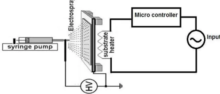
at room temperature and then aged for 2 h to get the required sol. Then the sol was taken in a syringe with the needle (2 mm dia). The solution loaded syringe is kept in the infusion pump (Model no: HQ-SPLF-04). Infusion pump could control the flow rate of the liquid specious. High potential of 10 kV is fed to the syringe needle and the substrate. The needle is given the phase supply with respect to the grounded substrate. The distance between the needle and substrate is kept 15 cm. And the flow rate is given 1 ml per hour to be sprayed on the ITO substrate. The temperature is maintained at 400 degree.
Fig. 1 – Schematic view of Elctro spraying set up
The X-ray analysis of both as deposited and annealed multilayer films were carried out using Shimadzu XRD-6000 X-ray Diffractometer. Here the films were exposed to Cu Kα source and the scattering angles were varied from 10-90. The surface Morphology of the films were analyzed using Scanning Electron Microscope (JSM 6390)The optical studies of the films were analyzed using UV-VIS-NIR spectrophotometer (Jasco-570 UV/VIS/NIR Spectrophotometer) in the range of 200 to 1200 nm. Photoluminescence studies were also carried out using Fluoromax-4 spectrophotometer in which Xenon is used as source with different excitation wavelength.
3. RESULTS AND DISCUSSION
3.1 Structural and surface morphological studies
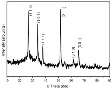
Fig. 2 shows the typical X-ray diffractogram (XRD) pattern of elctrosprayed SnO2 thin films prepared at 350. It is quite clear from this figure that the films are single-phase SnO2 with fine polycrystalline grains that are oriented along the (1 1 0), (1 0 1), (1 1 1), (2 1 1), (3 1 0) and (3 0 1) planes at 2 26.62, 33.87, 38.98, 51.66◦, 61.88◦ and 65.97respectively, where is the glancing angle of the peak. T. Serin et al. [8] observed nearly amorphous SnO2 films deposited at 300 C by spray pyrolysis method whereas in our work we got fine polycrystalline peaks at 300◦C. The crystalline size of the films were calculated using Scherer’s formula [9],
D 0.9 /( cos ), (1)
10 20 30 40 50 60 70 80 90 In te n si ty (a rb .u n it s)
2 Theta (deg)
(1 1 0 ) (1 0 1 ) (1 1 1 ) (2 1 1 ) (3 1 0
) (3 0
1
)
Fig. 2 –XRD pattern of electro sprayed SnO2 thin films
2 2 2
2 2 2
1 (h k ) l
d a c (2)
Where h, k, l are the Miller indices, a and c are the lattice constants and d
is the d-spacing calculated from Bragg relation,
d 0.5 /sin . (3)
Table 1 shows the structural parameters such as crystalline size and lattice constant of the SnO2 thin films prepared by electro spraying method at 300 C
Table 1– Structural parameters of electro sprayed SnO2 thin film
Film (h k l) 2 (deg) FWHM (deg) d-spacing Crystalline size (nm)
Lattice constant
(Å)
SnO2 (Tetragonal)
1 1 0 26.6280 0.5071 3.34495
1 0 1 33.8184 0.49160 2.64384 17 a 4.72 c 3.17 2 1 1 51.6634 0.47310 1.76784
The average crystalline size of 17 nm was calculated and the lattice constant of a 4.72, c 3.17 indicates that the prepared films match well with standard values. This leads to there is no stress induced effects on electro sprayed Tin oxide films at 300 C.
Fig. 3 – SEM image of electro sprayed SnO2thin films
The observed particle size from SEM is larger than the crystalline size from XRD and this is due to one particle consists of many crystallite in its.
3.2 UV-Vis spectroscopic studies
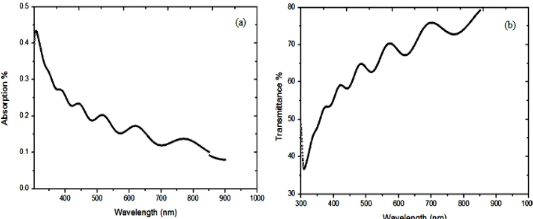
Fig. 3, 4 shows the absorption and transmittance spectra of SnO2 thin films prepared by electro spraying technique. Fig. 3. Shows the high transparency of 75 % in visible region (360-760 nm) and there are some interference peaks in the transmittance curve due to the influence of the thin film thickness. The similar result was already reported by J. Niet [13]. In addition, it can be seen that the absorption edge of the prepared sample is 320 nm and this result is in close agreement with the calculated optical band gap (3.5 eV) of the prepared films.
The optical band – gap determined by the equation [14],
h ~ (h –Eg)0.5 (4)
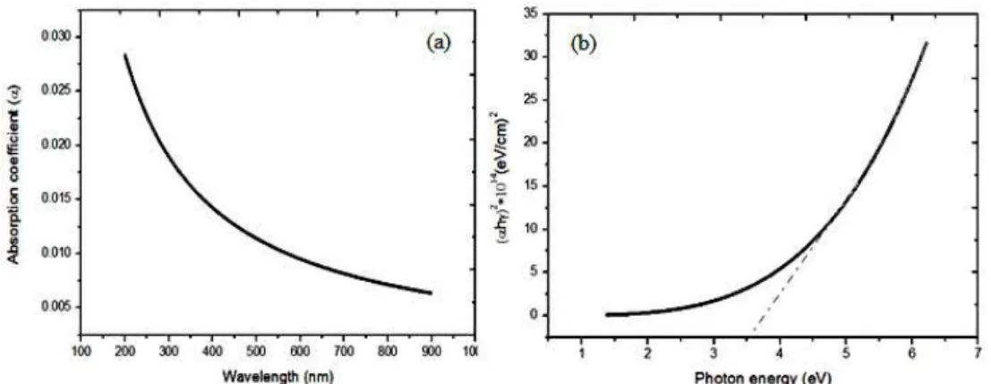
Where, g 4k/ is the absorption coefficient, h is the Planck’s constant, is frequency, Eg is the band gap energy and k is the extinction coefficient. The graph of absorption coefficient as a function of wavelength and the curve fitting of ( h )2 vs h are shown in Fig. 4a and 4b respectively.
Fig. 5– Absorption coefficient (a) and optical band gap (b) graph of electro sprayed SnO2 films
The extrapolation of the linear portion of the curve to ( h )2 0 gives the optical band gap value for the prepared films. The band gap energy of 3.5 eV was calculated which is larger than the bulk band gap (2.5-3 eV) of SnO2. The similar was reported by J. Podder et al. [15] for SnO2 films prepared by spray pyrolysis method.
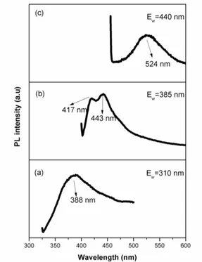
3.3 Photoluminescence analysis
Fig. 6, shows the photoluminescence spectra of electro sprayed Tin Oxide thin films excited at different wavelengths. The film excited at the wavelength of 310 nm is shown in Fig. 6a.The broad emission peak centered at 390 nm was observed due to band to band transition. There is no more feature was observed in this excited wavelength. However the broaden of the peak indicates the nanocrystalline effect of the films and this emission peaks attributes the blue emission band. The similar result was observed by Ameer Azam et al. [17]. The film excited at 385 nm is illustrated in Fig. 6b. The emission peaks centered at 442 nm 420 nm was well in agreement with the absorption spectra of the Tin oxide films (Fig. 4). The emission at 420 nm is attributed to the residual stresses within the tin dioxide Nanocrystals that originate from the lattice distortion. The emission observed at 442 nm is attributed to the Sn interstitials [18].
The film excited at 440 nm is shown in Fig. 6c. Two emission peaks observed at 526 nm and 675 nm attributed the oxygen deficiency [19]. Different types of oxygen vacancies exist, among them the 526 nm and 675 nm peaks are attributed to Vo+ and Vo2+ oxygen vacancies [20].
4. CONCLUSION
Fig. 6 – Photoluminescence spectra of Electro sprayed SnO2 films excited at various excitation wavelengths
bulk band gap of the materials. The blue emission band was observed by room temperature photoluminescence spectroscopy. Sn interstitials was observed from the peak centered at 442 nm.
REFERENCES
1. B.J. Lewis, D.C. Paine, MRS Bull.25, 22 (2000).
2. K. Omura, P. Veluchamy, M. Tsuji, T. Nishio, D. Mnrojono, J. Electrochem. Soc.
146, 2113 (1999).
3. S.J. Laverty, H. Feng, P Magurie, J. Electrochem. Soc.144, 2165 (1997). 4. A.V. Tadeev, G. Delabouglise, M. Labeau, Mater. Sci. Eng. B57, 76 (1998).
5. G. Korotcenkov, I. Blinov, V. Brinzari, J.R. Stetter, Sensor Actuat. B-Chem. 122, 519 (2007).
6. G. Leo, R. Rella, P. Siciliano, S. Capone, J.C. Alonso, V. Pankov, A. Ortiz, Sensor Actuat. B-Chem.58, 370 (1999).
7. A.N. Banerjee, R. Maity, S. Kundoo, K.K. Chattopadhyay, phys. status solidi a
201, 983 (2004).
8. T. Serin, N. Serin, S. Karadeniz, H. Sari, N. Tugluoglu, O. Pakma, J. Non-Cryst. Solids352, 209 (2006)
9. P.Y. Liu, J.F. Chen, W.D. Sun, Vacuum76, 7 (2004).
10. Z. Stryhal, J. Pavlka, S. Novak, A. Mackova, V. Pesrina, K. Veltruska, Vacuum
67, 665 (2002).
11. Jae-Ho Chung, Yong-Sahm Choe, Dae-Seung Kim, Thin Solid Films349, 126 (1999). 12. A. Guinier, X-Ray Diffraction (San Francio: CA: 1963).
14. F. Wooten, Optical properties of solids (Academic Press: New York: 1981).
15. A. S. Ahmed, M.M. Shafeeq, M.L. Singla, S. Tabassum, A.H. Naqvi, A. Azam, J. Lumin.131, 1 (2006).
16. S.S. Roy, J. Podder, J. Opt. Adv. Mater.12, 1479 (2010) (2010).
17. F. Gu, S.F. Wang, X.F. Cheng, S.F. Liu, G.J. Zhou et al., J. Cryst. Growth 262, 182 (2004).
18. Y. Sakurai, J. Non-Cryst. Solids352, 5391 (2006).
19. J.X. Zhou, M.S. Zhang, J.M. Hong, Z. Yin, Solid State Commun. 138, 242 (2006). 20. T. Krishnakumar, R. Jayaprakash, M. Parthibavarman, A.R. Phani, V.N. Singh,
![Optical Properties of MEH-PPV and MEH-PPV/ [6,6]-Phenyl C61-butyric Acid 3-ethylthiophene Ester Thin Films](data:image/gif;base64,R0lGODlhAQABAIAAAP///wAAACH5BAEAAAAALAAAAAABAAEAAAICRAEAOw==)