Growth and Characterization of HgI
2, PbI
2and PbI
2:HgI
2Layered
Semiconductors
E.R. Manoel, M.C.C. Custódio, F.E.G. Guimarães,
R.F. Bianchi, A.C. Hernandes
*Universidade de São Paulo, Instituto de Física de São Carlos, C.P. 369, 13560-970 São Carlos - SP, Brazil
*e-mail: hernandes@ifsc.sc.usp.br
Received: February 27, 1998; Revised: March 23, 1999
This paper presents a methodology for the preparation of α-HgI2 by Physical Vapor Transport and of PbI2 crystals using the Bridgman technique. The results of the growth of HgI2 diluted in PbI2 by the Bridgman technique are shown for the first time, its limit of solubility having been determined at 600 ppm of HgI2 in the PbI2 matrix. Optical absorption, photoluminescence and electrical conductivity measurements show that the crystals prepared are of good crystalline quality.
Keywords: mercuric iodide, lead iodide, crystal growth
1. Introduction
Increasing interest has been focusing on the search for high-energy resolution room temperature X-ray detectors. The development of single detector spectrometers and, lately, of multidetector array systems has been driven by the specific needs of space exploration and synchrotron radiation applications. Recently, layered semiconductors materials have been found to possess a number of properties that make them quite attractive for such applications. Mer-curic iodide (HgI2) and lead iodide (PbI2) crystals present an excellent response as X-ray and γ-ray detectors at room temperature. Their high density and high atomic number allow one to manufacture small, compact detectors with a very good volume-efficiency ratio1-4. The major advantage in using an HgI2 or PbI2 system in many applications is that they do not require liquid nitrogen for cooling, as opposed to most commercially available systems, which are com-posed of cryogenically cooled silicon or germanium X-ray detectors.
Several studies have been carried out on the properties, preparation and application of the HgI2 layered semicon-ductor compound and much progress has been made through improved purification of starting materials and growth techniques5-7. However, good PbI2 crystals have only recently been prepared8. In this work, we present a methodology for the preparation of α-HgI2 by Physical Vapor Transport and for PbI2 crystals using the Bridgman
technique. We also show, for the first time, the results of the growth of HgI2 diluted in PbI2 by the Bridgman tech-nique. In this specific case, the solubility limit was deter-mined and some electric, structural and optical properties were measured.
2. Experimental Procedure
2.1. Purification and crystal growth
α-HgI2
70 h were necessary to evaporate all the HgI2, which was then deposited in the cold extremity of the ampoule. In each cycle, the impurities (black from red HgI2 Fluka and gray-ish from Aldrich) deposited at the hot extremity were eliminated by sealing off part of the glass ampoule. After each cycle, the amount of the impurities decreased drasti-cally. Black and grayish impurities were associated to amorphous carbon and hydrocarbon, as suggested by Piechotka and Kaldis6.
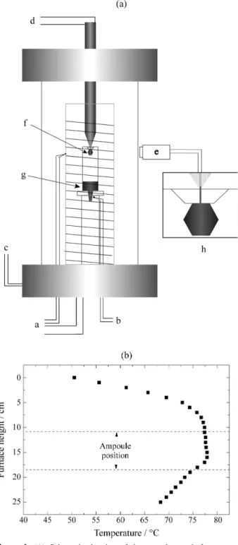
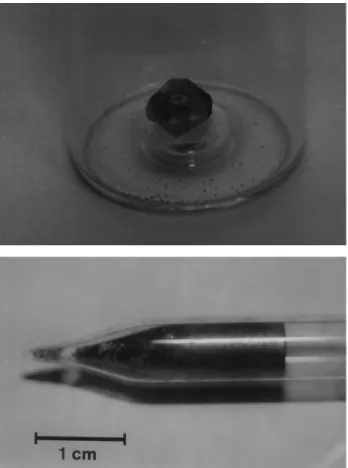
After the purification process, the mercuric iodide was used as a source in crystal growth runs. Every growth experiments were performed by the Physical Vapor Trans-port (PVT) technique9, in a homemade equipment shown in Fig. 1A.This system consisted of a transparent resistive furnace equipped with an 808 Eurotherm temperature con-troller. Vacuum was used as thermal insulation and the typical temperature fluctuation was 0.5° Celsius. A cold finger was used as a heat exchanger with a temperature control better than ±0.3 °C. The temperature profile of our crystal growth system (Fig. 1B) was measured using a Chromel-Alumel thermocouple when the furnace was empty, that is, without the ampoule. The ampoule with red mercuric iodide was placed in an area of the furnace where the temperature was approximately constant (Fig. 1B). A small area of the cold finger was put in contact with the growth ampoule in a predetermined position. The tempera-ture gradient established in this area was responsible for the nucleation process. Seed selection was carried out by the trial and error procedure. The following growth of the red HgI2 crystal was possible through a cooling temperature program applied to the cold finger. The optimal mass transport responsible for growth was achieved through maximization of the aspect ratio (height/ radius of am-poule). After some tests, we were able to grow good quality crystals of reasonable size (0.6 cm3) and with a very well defined external morphology. Figure 2A shows one of the crystals obtained by this technique.
PbI2 and PbI2: HgI2
Lead iodide is a more stable compound than mercuric iodide due to its lower vapor pressure and its stable crystal-line structure up to its melting point. These two charac-teristics make it easier to prepare than red HgI2. In our experiments we used PbI2 from Johnson Matthey Co. (99.999% metal pure) which was purified by recrystalliza-tion to avoid organic impurities.
A quartz ampoule (8 mm in internal diameter and 95 mm in length) was used in all the crystal growing runs. It was washed with detergent and distilled water, chemically cleaned in a HF and HNO3 solution (1:1 in volume) for approximately 15 min and thermally treated at 800 °C under high vacuum conditions. After this step, the recrystallized PbI2 was placed in the ampoule, sealed under high vacuum (~10-5 Torr) and put into the Bridgman furnace.
The Bridgman equipment had previously been built and thermally characterized10. The axial temperature gradient measured during crystal growth was 35 °C/cm. All the PbI2 prepared in our system were yellowish and transparent and easily cleaved in the direction perpendicular to the c crys-tallographic axis. Bubbles appeared only on its external
surface and there was no adhesion to the quartz ampoule. This last characteristic is an indication of the absence of OH- impurities in our experiments, as suggested by Eck-stein et al.11. Figure 2B shows a PbI2 single crystal grown under the experimental conditions described above.
PbI2: HgI2 crystals were grown at five different nominal concentrations (50000 ppm, 5000 ppm, 1100 ppm, 680 ppm and 600 ppm) also following the experimental routine of the pure lead iodide. A segregated phase of mercuric iodide was observed in most of the experiments, and it was asso-ciated to the structural difference between PbI2 (hexagonal structure) and HgI2 (tetragonal structure). Indeed, a large amount of HgI2 in the bulk and on the surface of the grown crystal was detected at a high nominal concentration. A small amount of segregated phase was detected in the experiment with 680 ppm of mercuric iodide. On the other hand, no segregated phase was detected with a nominal concentration of 600 ppm of red HgI2. These crystals were transparent and were reddish in color. It was assumed that 600 ppm of HgI2 in the liquid phase is the solubility limit for PbI2 crystals.
2.2. Characterization
Photoluminescence (PL) measurements were carried out using an Ar ion laser tuned to 458 nm. The samples were
fixed with teflon tape on a cooled copper finger of a closed-cycle helium cryostat to avoid any chemical reac-tion, and cooled to a temperature of about 15 K. The PL radiation was dispersed in a 0.5 m monochromator with 0.01 nm resolution and detected by a photomultiplier tube using conventional lock-in detection. All the experiments were carried out under very low excitation intensities to avoid thermal heating of the sample and identical optical paths.
The optical band gap of the crystals was determined by absorption measurements, in the visible spectral range, at room temperature (300 K), using Cary 17 equipment.
The DC conductivity measurements were made of all grown crystals at room temperature using a voltage source and an electrometer to detect the current. The electrical contacts were made by pressing the sample between brass plates.
3. Results and Discussion
The low temperature PL spectra of HgI2 samples grown after three different purification procedures are shown in Fig. 3. In (a), a seed was obtained after one cycle of purification, in (b) a grain of a polycrystalline material was obtained from two purification cycles, and in (c) a single crystal was obtained from three purification cycles. The last two samples were grown by the PVT method. The results Figure 2. (A) Mercuric iodide single crystal grown by PVT method. (B)
PbI2 crystal grown by Bridgman technique.
show the effect of purification on crystalline quality. Four bands were observed in the single purification cycle. The broad III and IV bands located at 1.844 eV and 1.646 eV, respectively, are associated to impurities. Band IV and three other bands have already been analyzed by Merz et al.12. A comparison of their spectra shows that our single cycle purification spectrum is very similar, with a coinci-dence of bands I, (2. 335 eV) II (2.216 eV) and IV (1.640 eV). Merz et al. also labeled a broad band, present only in raw material and located at 2.000 eV, as B3. This band disappeared after the first purification cycle, and was also absent in our spectra. The major difference in our spectra is the presence of the band located at 1.844 eV. We attrib-uted this band to copper, as a result of an accidental contact of the sample to the copper of the cold finger, although teflon tape was used for isolation. This attribution was based on the study performed by Bao et al.13, who first attributed this band to copper. They studied the photolumi-nescence spectra taken from the same spot on an HgI2 crystal obtained before and after a semitransparent Cu layer was deposited, where and a broad band centered at 672.0 nm (1.844 eV) appeared after the deposition
A comparison of the (a), (b), and (c) spectra (Fig. 3) shows that the sample with two purification cycles does not present the broad band that is further away from the band edge. Moreover, the band II to band I ratio decreased. There was a further decrease in band II to band I ratio with three purification cycles, and the intensity of band II was also considerably lower. The band II to band I ratio and the absolute intensity of band II were associated to changes in stoichiometry by Merz et al.12 and Schieber et al.14. They demonstrated that both factors increased in successive sub-limation runs, when each run was performed under dy-namic vacuum conditions, which might reduce the iodine concentration by preferential removal of the more volatile species. Thus, our results show that the triple purification cycle sample has no impurity bands and is not iodine deficient, as a result of carrying out the sublimation proc-esses in closed tubes. Another feature of these spectra is that band I is, in fact, the predominant line of a great set of lines in the region near the band edge. This region was studied by several authors15,16, and Bao et al., in 199017, identified 26 emission lines from 2.343 eV (529.0 nm) to 2.295 eV (540.0 nm), the predominant line, located at 2.335 eV, being due to zero-phonon line emission of polariton A15, and other extremely near lines, which are not resolved in our spectrum, are due to bound excitons.
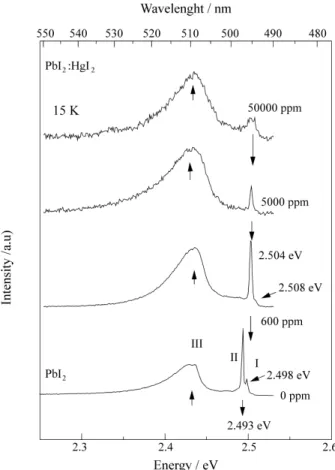
Figure 4 illustrates the PL emissions near the band edge for PbI2:HgI2 samples containing nominally 600 ppm, 5000 ppm and 50000 ppm of HgI2 in the source materials. The same figure also shows a spectrum of pure PbI2,for com-parison. It should be pointed out that although doped PbI2 samples are more reddish than the pure ones, the PL spectra do not present any detectable red shift. In the 2H polytype
level recombination19 and this band shifts to 2.438 eV in doped samples.
The results of electrical conductivity obtained for α -HgI2 and PbI2 samples were 1 x 10-13Ω-1 cm-1and 3 x 10-12
Ω-1 cm-1, respectively, coinciding with the best values found in the literature21. The electrical conductivities at room temperature in the diluted crystals presented a disper-sion of three orders of magnitude (10-14 to 10-11Ω-1 cm-1), and the sample containing 600 ppm of HgI2 was the most resistive one, with electrical conductivity of 5 x 10-14Ω-1 cm-1, the smallest obtained value for this group of materials. The optical band gap energies determined were 2.10 eV to α-HgI2 and 2.28 eV to pure PbI2. These results are very close to the previously published values13. The values ob-tained for the HgI2 diluted in PbI2 crystals do not present any difference in comparison to the pure crystal.
5. Conclusions
α-HgI2, PbI2 and diluted doped PbI2 samples were grown, the first by Physical Vapor Transport and the second and third by the Bridgman method. The characterization techniques employed showed that the crystals are of good quality. The PL results from the mercuric iodide samples showed that, after 3 purification cycles, the exciton emis-sion line is sharp and with a high intensity. Moreover, no impurity band was observed and the material was not iodine deficient. Analysis of the PL spectra of doped PbI2 samples indicated that the introduction of mercuric iodide in lead iodide lattice changed the polytype from 2H to 4H and destroyed the structural quality. It was, nonetheless, possi-ble to determine the solubility limit at 600 ppm of HgI2, the free exciton line for this sample was still seen in the spec-trum and the sample presented the lowest DC conductivity (5 10-14Ω-1 cm-1) of this type of material. All the samples measured were very resistive, with values of 10-13Ω-1 cm-1 of mercuric iodide and 3 10-12Ω-1 cm-1 of lead iodide, which coincide with the best values reported in the literature. Furthermore, the values obtained for the optical band gap at room temperature are in good agreement with the ones reported previously.
Acknowledgments
The authors wish to express their appreciation for the financial support provided by the Brazilian agencies FAPESP, CNPq, CAPES and FINEP.
References
1. Iwanczyk, J.S.; Wang, Y.J.; Bradley, J.G.; Conley, J.M.; Albee, A.L.; Economou; T.E. IEEE Trans. on Nuclear Sci., v. 36, n. 1, p. 841-845, 1989.
2. Olmos, P.; Perez, J.M.; Diegues, E.; Serrano, M.D. J. Phys. D: Appl. Phys., v. 27, p. 2251-2257, 1994. 3. Eckstein, J.; Erler, B.; Eiche, C.; Benz, K.W. J.Cryst.
Growth, v. 131, p. 453-456, 1993.
4. Li, Z.; Li, W.; Liu, J.; Zhao, B.; Zhu, S.; Xu, H.; Yuan, H. J. Cryst. Growth, v. 156, p. 86-90, 1995.
5. Manoel, E.R. Dissertação de Mestrado, IFSC, USP, 1997.
6. Piechotka, M.; Kaldis, E. Final Report ESA Contract, Zurich, Switzeland, 1991.
7. Piechotka, M.; Kaldis, E. Nuclear Instr. and Methods in Phys. Research, v. A322, p. 387, 1992.
8. Chaudhary, S.K.; Trigunayat J. Cryst. Growth, v. 62, p. 398-400, 1983.
9. van den Berg, L.; Schnepple, W.F. Nuclear Instr. and Methods in Phys. Research, v. A283, p. 335-338, 1989.
10. Custódio, M.C.C. Tese de Doutoramento, IF, USP, 1997.
11. Eckstein, J.; Erler, B.; Benz, K.W. Mat. Res. Bull., v. 27, p. 533-544, 1992.
12. Merz, J.L.; Wu, Z.L.; van den berg, L.; Schenepple, W.F. Nucl. Inst. Meth., v. 213, p. 51, 1983.
13. Bao, X.J.; Schlesinger, T.E.; James, R.B.; Stulen, R.H.; Ortale, C.; van den Berg, L. J. Appl. Phys., v. 67, n. 12, 1990.
14. Schieber, M.; Roth, M.; Schnepple, W.F. J. Cryst. Growth, v. 65, p. 353-364, 1983.
15. Goto, T.; Nishina, Y. Solid State Commun., v. 25, p. 123-125, 1978.
16. Novikov, B.V.; Pimonenko, M.M. Sov. Phys. Semic., v. 4, p. 1785, 1971.
17. Bao, X.J.; Schlesinger, T.E.; James, R.B.; Ortale, C.; van den Berg, L. J. Appl. Phys., v. 68, n. 6, 1990. 18. Gähwiller, C.H.; Harbeke, G. Phys. Rev., v. 185, p.
1141, 1969.
19. Lévy, F.; Mercier, A.; Voitchovsky, J.P. Solid State Commun., v. 15, p. 819-822, 1974.
20. Guimarães, F.E.G.; Manoel, E.R.; Sabino, J.R.; Her-nandes, A.C., Braz. J. Phys., v. 27/A, n. 4, 1997. 21. Minder, R.; Ottaviani, G.; Canali, C. J. Phys. Chem.