UNIVERSIDADE FEDERAL DE MINAS GERAIS DEPARTAMENTO DE FÍSICA
THIAGO HENRIQUE RODRIGUES DA CUNHA
Chemical Vapor Deposition of Graphene at Very Low
Pressures
ii THIAGO HENRIQUE RODRIGUES DA CUNHA
Chemical Vapor Deposition of Graphene at Very Low
Pressures
Tese apresentada à Universidade Federal de Minas Gerais como requisito parcial para a obtenção do grau de Doutor Em Física.
Área de Concentração: Física da Matéria Condensada Orientador: André Santarosa Ferlauto
Belo Horizonte
iii
Agradecimentos
Aos meus pais que sempre primaram pela minha educação, me oferecendo oportunidades e incentivo.
Ao meu orientador André Ferlauto pelas palavras lúcidas e de estímulo que contribuíram tanto para o meu amadurecimento profissional quanto pessoal. O desfecho deste trabalho se deve em muito as suas críticas e sugestões.
Ao Sérgio pela atenção e paciência em compartilhar seu vasto conhecimento prático. A qualidade dos resultados apresentados neste trabalho não seria a mesma sem seus conselhos e auxilio.
Aos professores Rodrigo Gribel e Luís Orlando pelas sugestões, apoio e amizade. À minha companheira Jaqueline pelo carinho, companheirismo e por me inspirar até o desfecho desta tese.
Aos meus amigos de Piumhi, Viçosa e Belo Horizonte, os quais não irei citar aqui por medo de cometer uma injustiça esquecendo de algum nome.
iv
Contents
List of Figures………...vi
Resumo ...………xii
Abstract ...………...xiii
1 Introduction ... 1
2 Bibliography Review... 3
2.1 Graphene Fundamentals ... 3
2.1.1 Graphene Chemistry ... 3
2.1.2 Electronic Band Structure of Graphene ... 5
2.1.3 Graphene Production ... 6
2.2 Crystal Growth ... 8
2.2.1 Chemical Vapor Deposition of Thin Films ... 8
2.2.2 Crystal Growth Theories ... 11
2.3 Precursor Catalysis ... 19
2.3.1 General Aspects of the Catalytic Mechanism ... 19
2.3.2 Activation Energy of Precursor Decomposition ... 22
2.4 Graphene Growth on Metal Surfaces ... 23
2.4.1 Graphene Growth on Ni ... 23
2.4.2 Graphene growth on Ru ... 24
2.4.3 Graphene growth on Cu ... 26
3 Experimental Setup and Characterization Tools ... 34
3.1 CVD Reactor ... 34
3.2 Optical Microscopy Characterizations ... 37
3.3 Raman Spectroscopy of Graphene ... 38
3.4 Electron Backscatter Diffraction ... 41
v
3.4.2 EBSD Data – Inverse Figure Pole ... 44
3.5 Transferring Graphene ... 46
3.5.1 Cu dissolution transfer method ... 46
3.5.2 Electrolysis induced H2 bubbling transfer method ... 47
3.6 Electrical Characterizations ... 48
3.6.1 Graphene Field Effect Transistor (G-FET) ... 48
3.6.2 Device Fabrication ... 52
4 Results and Discussion ... 54
4.1 Cu-Catalyzed Methane-Based graphene CVD ... 54
4.1.1 The Temperature Dependence of Graphene Films ... 54
4.1.2 Film Strain ... 56
4.1.3 Film Electrical Proprieties ... 60
4.2 Graphene Growth at Very Low Pressure ... 63
4.2.1 The Liquid Precursor ... 63
4.2.2 The impact of substrate surface self-diffusion in domain shape ... 65
5 Conclusion ... 80
vi
List of Figures
Figure 2-1 – sp2 hybridization. Reproduced from [24]. ... 3
Figure 2-2 - (a) Graphene honeycomb lattice. (b) Reciprocal lattice of the triangular lattice. The shaded region
ep ese ts the fi st B illoui zo e BZ , ithits e t e Γ and the two inequivalent corners K (black squares) and
K′ hite s ua es . Rep odu ed f o [ 5]. ... 4
Figure 2-3 - Electronic dispersion of graphene. The conduction band and the valence band touch each other at K
a d K’ poi ts. The zoo sho s that the dispe sio elatio lose to these poi ts ese bles the energy spectrum
of massless Dirac particles. Reproduced from [26]... 6
Figure 2-4 - Several methods of mass-production of graphene which allow a wide choice in terms of size, quality and price for any particular application. Reproduced from [8]. ... 7
Figure 2-5. Schematic representation of the fundamental transport and reaction steps underlying CVD. Since no dissolution of carbon is considered, this model can be only applied to metals with low carbon solubility such as Cu or for lower temperature CVD in which carbon solubility is also insignificant. Reproduced from [30]. ... 10
Figure 2-6 - Deposition rate as a function of temperature. Reproduced from [31]. ... 10
Figure 2-7. Nucleation and growth mechanism of graphene on Cu. The decomposition of methane leads to supersaturation of carbon adspecies at the Cu surface. When ccu reaches a critical supersaturation point (cnuc)
graphene domains nucleate and begin to grow (i). The growth proceeds (ii) until the amount of superstaurated carbon species are consumed (iii) or until the domains merge together full covering the surface of Cu (iv). Reproduced from reference [37] ... 12
Figure 2-8 - Surface free energy plotted as a function of the angle θ describing the normal directions to the {hkl} planes in the Wulff construction. The equilibrium shape of the crystal is given by the dash-dotted curve. Reproduced from [39]. ... 13
Figure 2-9 - The various atomic positions in the KVS model. ... 14
Figure 2-10 – Vicinal surface considered in BCF theory. (a) The values ± are the adatom densities on the right
+ a d left − sides of the step; Ki eti e ha is s go e i g the g o th; D is the diffusio o sta t, F is the
deposition flux, 𝜏 is the desorption time, and 𝑣 ± are step attachment coefficients from the lower and upper sides, respectively. Reproduced from [43, 44]. ... 15
vii
Figure 2-12 – (a) AFM image of a screw dislocation during the growth of an insulin crystal; (b) STM image of Si(111) surface showing three macrosteps formed from bunching of many monatomic steps; (c) Hole created on Si by a lithographic process and filled in after a annealing step at 1300ºC. The 3-fold crystallographic symmetry of the substrate is expressed in the pattern of steps generated around the filled hole. Reproduced from [42, 45] ... 17
Figure 2-13. Carbon adatom density modeled using rate equations (black curve) compared with the corresponding LEEM data of Loginova et al. [48] (red data points). Reproduced from [47]. ... 19
Figure 2-14 - Reaction mechanisms in CVD graphene. The blue arrows indicate the more probable (but not unique) reaction mechanisms. Reaction of type A: adsorption-desorption. B: dehydrogenation-hydrogenation. C: surface diffusion or migration (more favorable for dimers C2). D: dimerization with or without simultaneous
dehydrogenation (Dimers with hydrogen are not stable at high temperatures). E: polymerization - (cracking) decomposition. F: aromatization – decomposition. G: decomposition of aromatics. The green arrows indicate reactions with hydrogen. Reproduced from reference [29]. ... 20
Figure 2-15. Schematic diagrams of graphene growth mechanism on Ni(111) (a) and polycrystalline Ni surface (d). Optical image of graphene grown on Ni(111) (b) and polycrystalline Ni (e). Maps of I2D/IG of Raman spectra
collected on the Ni(111) surface (c) and on the polycrystalline Ni surface (f). Reproduced from reference [73] .. 24
Figure 2-16 – (a) Island growth rate as function of monomer concentration; (b) Time evolution of C monomer concentration during C deposition. Nucleation start to occur at the steps edges of Ru substrate, and then it takes place at the Ru terraces at higher C concentrations. Reproduced from [48]. ... 25
Figure 2-17 - In situ STM scans showing: (a-b) the growth of graphene (blue) across the steps of the Ru(0001) surface (orange) at 665º C; (c-d) graphene growth at higher temperatures (or low pressures) accompanied by the extension of the underneath Ru terrace. e) Extensive faceting of the Ru surface induced by the above graphene layer. Reproduced from [74]. ... 26
Figure 2-18. (a-c) SEM image showing an array of seed crystals patterned on Cu foil by e-beam lithography. (d) SEM image of a seeded array of graphene domains next to a randomly-nucleated set of graphene domains in an area without seeds. Scale bars in (a-c) are 10 µm and the scale bar in (d) is 200 µm. Reproduced from [12]. ... 27
Figure 2-19. (a) APCVD growth of graphene at 1050 °C with a linear increase of temperature of the polystyrene source and total reactant gas flow. (b-d) SEM image of the obtained hexagon-shaped graphene domains. Reproduced from [65]. ... 28
Figure 2-20. Graphene island morphology dependence on H2:CH4 in APCVD. First, second, and third columns
represent the island structure on Cu(100), Cu(110), and Cu(111). Reproduced from [16]. ... 29
viii
Figure 2-22. (a-d) Shape and orientation dependence of LPCVD graphene domains on polycrystalline Cu. (e,f,g,h) SEM images of representative LPCVD graphene domain shapes grown on Cu{101}, Cu{001}, Cu{103}, and
orientations close to Cu{111}, e.g., Cu{769}, respectively. ... 32
Figure 2-23. Computational modeling of graphene clusters on Cu{101}, Cu{001}, and Cu{111}. Red circles correspond to the surface atoms (high electron density), while regions with depleted electron density are equivalent to available adatomsites (labeled A). Strong one-to-one hybridization occurs along the Cu direction between the electron orbitals of the zigzag edge atoms of C28 and Cu surface atoms on Cu(101) and Cu(001) indicated by yellow lines in g and h. Weaker one-to-two atom bonding between one C and two Cu atoms is observed on Cu(111). Reproduced from [18]. ... 33
Figure 3-1 – CVD reactor for graphene growth ... 34
Figure 3-2 – (a) Commercial sample heater; (b) Homemade graphite heater. ... 36
Figure 3-3 – Photography of the system built for graphene chemical vapor deposition. ... 36
Figure 3-4 – Formation of a continuous graphene film by coalescence of monocrystalline domains of graphene. ... 37
Figure 3-5 – Optical Image of graphene on Cu: (a) As-grown; (b) thermally oxidized in air after the growth. ... 37
Figure 3-6 - Energy-level diagram showing the states involved in Raman signal. ... 38
Figure 3-7 – (a) Phonon dispersion of monolayer graphene in the high symmetric directions calculated using the tight-biding method [79]. (b) Vibrations of the two atoms of the unit cell of monolayer graphene that correspond to the si pho o a hes at the Γ poi t. Rep odu ed f o [78]. ... 39
Figure 3-8 - (a) First-order Raman process which gives rise to the G band; (b) two-phonon second-order Raman spectral processes giving rise to the 2D band; (c) One-phonon second-order Raman process giving rise to the D band; (d) Schematic view of a possible triple resonance giving rise to the 2D Raman band in graphene. Adapted from [77]. ... 40
Figure 3-9 – Basic EBSD setup... 42
Figure 3-10 – (a) Bragg -reflection of electrons from a local electron source Q at the (010) and (021) lattice planes leading to a signal on the detector screen; (b) Position of the Kossel cones of a lattice plane in respect to the detector. Adapted from refs [83] [84]. ... 42
Figure 3-11 - Sequential steps of EBSD processing. (a) Kikuchi bands of the diffraction pattern collected from silicon; (b) Hough transform of the Kikuchi bands obtained in (a); (c) Identification and fitting of the points obtained in (b) by comparing it with the values known from reference tables. (d) Inverse Hough transform of the peaks found in (c). (e) Original diffraction pattern indexed by the Miller indices. Reproduced from Ref. [84]. .... 43
ix
Figure 3-13 -(a) Projection of a point P on the surface of a sphere onto the equatorial plane at p; (b) The stereographic projection of the point P; (c) A cubic unit cell placed at the center of the projection sphere with its six {001} plane normals (poles) highlighted; (d) A stereographic projection of the directions shown in (c). Reproduced from [84]. ... 45
Figure 3-14 – Construction of the inverse pole figure. Only one stereographic triangle is required to describe a family of equivalent crystallographic directions because all triangles in the stereographic projection are symmetrically equivalent. Adapted from [84]. ... 46
Figure 3-15 – Schematic illustration of graphene transfer from Cu foil to an arbitrary substrate. Reproduced from ... 47
Figure 3-16 - H2 bubbling separation of the frame/PMMA/graphene from the Cu foil induced by H2O electrolysis.
Adapted from [85]. ... 48
Figure 3-17 – Graphene based back-gated field effect transistor [87]. ... 49
Figure 3-18 - typical transfer curve for a single-layer graphene transistor: channel resistivity (blue line) and channel conductivity (red dashed line) vs. gate voltage. Adapted from [89]. ... 51
Figure 3-19 – Sequential steps of G-FET production. ... 53
Figure 4-1 - SEM images of graphene domains grown at different temperatures. ... 54
Figure 4-2 - Raman spectra of graphene films grown at different temperatures. The photoluminescence of the copper substrate produces a strong background in the Raman spectra. ... 55
Figure 4-3 - Comparison of bad Lorentzian fit and good Voigt fit of the same spectrum. ... 56
Figure 4-4 – (a) Sketch of the Cu substrate positioned over the graphite heater and typical SEM image of the backside of the substrate after the growth. (b) Optical images of the graphene grown along the backside of the copper foil. Graphene fully covers the copper at the edge of the sample (x=30 µm), whereas individual grains covers the middle of the foil (x=730 µm), where less carbon had access. ... 57
Figure 4-5 - Raman spectra in the D-G region taken at the same locations as the images shown in Figure 4-4. The G peak blue shifts about 10 cm-1 from the edge of the sample to middle where the individual grains can be seen
on copper substrate. The sample position axis represent how far away from one of the edges the spectra was acquired. A D peak can be seen to appear in the region where the individual grains are grown. This is consequence of more graphene edges being probed... 58
Figure 4-6 - Raman spectra in the 2D region taken at the same locations as the images shown in Figure 4-4 The 2D peak blue shifts about 30 cm-1 from the edge of the sample to the middle, where the individual grains can be
seen on copper substrate. ... 58
x
Figure 4-8 – (a) Graphene film and (b) graphene monocrystalline domains transferred to SiO2/Si. The achievement
of large graphene single domains as showed in (b) is discussed in details in section 4.2. ... 61
Figure 4-9 – Back-gated graphene field effect transistor (GFET). See section 3.6.2. for further details. ... 61
Figure 4-10 – Experimental setup for electrical measurements ... 62
Figure 4-11 - Transconductance curve of the device shown in Figure 4-9. ... 62
Figure 4-12- (a) Optical image of large graphene domains grown at low pressure and high temperature (960 ºC) using paraffinic oil; (b) Raman Spectra of a single graphene domain. For clarity, the strong background due to Cu photoluminescence was subtracted from the Raman spectra ... 65
Figure 4-13 – EBSD map of a typical Cu foil used during graphene growth. ... 66
Figure 4-14 - SEM image and the corresponding EBSD data (inset) of graphene grown over as-receveid Cu foil on Cu(113) surface at 960 ºC. ... 66
Figure 4-15 – (a) Optical images of graphene domains grown on as-received Cu foil. The growth temperature was 950 ºC and the precursor partial pressure 5 x 10⁻⁶ Torr. ... 67
Figure 4-16 - (a) Average growth rates of graphene domains shown in Figure 4-15; (b) Raman spectra of graphene domains grown in different Cu faces. The fluorescence background signal due the Cu substrate was removed from the total spectra. ... 68
Figure 4-17 – Cu crystallographic surfaces ... 69
Figure 4-18 - SEM image of graphene domains at different stages (T = 950 ºC). Due to large deviations in nucleation time, various phases of growth can be observed in the same sample. The scale bar in the inset is 200 nm. ... 69
Figure 4-19 - Temperature dependence of graphene shape on Cu(101). The growth temperatures were (a) 920 ºC, (b) 940 ºC, (c) 960 ºC, and (d) 980 ºC. ... 71
Figure 4-20 – (a) Formation of Cu hillocks at 980º C. (b) Topologic profile of the exposed Cu surface after graphene growth. ... 71
Figure 4-21 - Arrhenius plot of the temperature dependence of (a) density of graphene nuclei measured at the (101) Cu Surface, (b) temperature dependence of surface self-diffusion on Cu (101) surface. Reprinted from J. Phys. and Chem. Ref. Data 2, 643-655 (1973). ... 73
Figure 4-22 – Surface diffusion of copper on copper. Reproduced from [115]. ... 74
Figure 4-23 - The effect of oxygen on graphene growth kinetics. SEM images of graphene domains grown with and without the assistance of oxygen. Reproduced from [127]. ... 75
xi
ele ated Cu te a e p o ess . This auses the i ease of the a ie see s a o adspe ies a i i g at
the domain edges, reducing their attachment probability (process 2). In the meantime, due to the high temperature, a high fraction of Cu atoms from flat terraces have enough energy to detach and to diffuse as loosely-bound adatoms (process 3). Diffusive Cu adatoms that impinge upon the steps retained by graphene domains can be incorporated extending the Cu terraces in accordance with the local Cu symmetry (process 4). The shape of the Cu terraces defines the most probable directions at which the incoming carbon adspecies can attach to the graphene edge (process 5). ... 76
Figure 4-25 – AFM image of a graphene domain grown on Cu at 960 ºC and × − Torr ... 77 Figure 4-26 - Schematic view of the proposed growth model. Ds is the surface diffusio te so , τs is the life time of
xii
Resumo
xiii
Abstract
1
1
Introduction
Graphene is, in simple terms, a single atomic layer of graphite. The existence of graphene itself is remarkable because before it “discovery” in 2004, when Novoselov and Geim [1] used adhesive tape to separate graphene sheets from graphite flakes, the stability of 2D crystals was uncertain. In fact, it was theoretically predicted [2, 3] that thermal fluctuations would destroy the long-range order of such crystals at non-zero temperature. The discovery of this 2D material triggered thousands of publications, largely because of its so-called extraordinary properties: high electron mobility [4], mechanical strength 200 times greater than steel [5], high thermal conductivity [6], and substantial absorption of white light, i.e. 2.3% (which is very high considering it is only one atom thick) [7]. Therefore, graphene have potential to be integrated into a huge number of applications. However, it has yet to be developed a production method that yields graphene layers with of well-defined properties in large quantities with competitive costs.
2 the substrate, there have been various LPCVD studies that provide evidence of a relationship between the shape, symmetry and orientation of graphene domains and the underlying lattice of Cu grains. [16, 17, 18, 19]
Until now, the proposed growth models to explain the observed relationship between the graphene domains and the underlying Cu crystals in LPCVD were based either on anisotropic attachment of carbon species to the graphene edges [16, 18, 20] or on anisotropic carbon diffusion over the substrate surface [21] or both [22].However, in these descriptions, Cu surface self-diffusion was not taken into account, even though it is expected to be considerable at typical growth temperatures, which are close to the Cu melting point. Thus, despite the considerable
number of theoretical and experimental efforts since the pioneer work of Ruoff’s group in 2009,
[9] yet there is not a consensus about the ruling mechanisms of graphene CVD on Cu due the lack of a single theory which explains features observed in LPCVD that are not present in APCVD.
In this thesis, we have performed a study of very low pressure CVD of graphene on Cu using a liquid source in a cold wall reactor. In chapter 2, we provide a brief description of the graphene structure, followed by an overview of the potential methods for scale-production of graphene. We emphasize in the chemical vapor deposition, treating either the general aspects of the CVD process as the growth models that were invoked to explain the growth mechanism of graphene. We also present some interesting findings from the literature concerning the CVD of graphene over different metals.
3
2
Bibliography Review
2.1
Graphene Fundamentals
2.1.1
Graphene Chemistry
Carbon, the basic building block of graphene, has six electrons arranged in the 1s2 2s2 2p2
configuration, wherein 2 electrons fill the inner shell 1s and 4 electrons occupy the outer shell
of 2s and 2p orbitals. It turns out, however, that the presence of other atoms in the neighborhood of the C atom (e.g., hydrogen, oxygen, carbon) induces the hybridization of the 2s and 2p states. In particular, the superposition of the 2s orbital with two 2p orbitals, say 2px and 2py, leads to
the formation of the bond responsible for the hexagonal planar structure of graphene. The remained unhybridised pz orbital is perpendicular to the plane and bind with the neighboring
carbon atoms, forming a π band. A typical manner of parameterize these orthogonal hybridized s-p states is the following [23]:
| ⟩ =
√ | ⟩ + √ | ⟩ eq. 2-1
| ⟩ =
√ | ⟩ − √ | ⟩ − √ | 𝑌⟩ eq. 2-2
| ⟩ =
√ | ⟩ − √ | ⟩ + √ | 𝑌⟩ eq. 2-3
These atomic orbitals (AOs) are shown in Figure 2-1. In free space, the orbitals | ⟩, | ⟩ and | ⟩ are degenerated [23]:
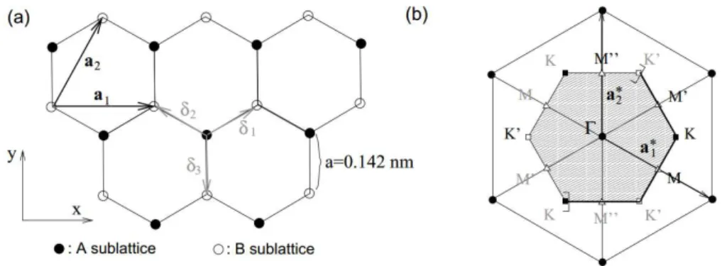
4 Carbon atoms condense in graphene in a honeycomb lattice because three hybrid sp2 orbitals, having a mutual 120o angle in the xy-plane, are induced in each atom. The honeycomb lattice is not a Bravais lattice since two neighboring sites are not equivalent, i.e. they cannot be connected by a lattice vector. Nevertheless, the honeycomb lattice can be viewed as a triangular Bravais lattice with a two-atom basis (A and B) as depicted in Figure 2-2.
Figure 2-2 - (a) Graphene honeycomb lattice. (b) Reciprocal lattice of the triangular lattice. The shaded region
represents the first Brillouin zone (BZ), withits centre Γ and the two inequivalent corners K (black squares) and
K′(white squares). Reproduced from [25].
The triangular Bravais lattice shown in Figure 2-2(a) is spanned by the basis vectors:
𝒂 = √ 𝑎𝐞 and 𝒂 =√ 𝑎(𝐞 + √ 𝐞 ) eq. 2-4
whilst the nearest neighbors vectors are denoted by:
𝜹 = 𝑎(√ 𝐞 + 𝐞 ), 𝜹 =𝑎(−√ 𝐞 + 𝐞 ) and 𝜹 = −𝑎𝐞 eq. 2-5
The first Brillouin zone is the region enclosed by the sets of planes that are perpendicular bisectors to the reciprocal lattice vectors:
𝒂∗ = 𝜋
√ 𝑎(𝐞 −
𝐞
√ ) and 𝒂
∗ = 𝜋
𝑎 𝐞 eq. 2-6
5
2.1.2
Electronic Band Structure of Graphene
In graphene, three electrons per carbon atom are involved in the formation of strong
covalent bonds (in three hybridized sp2 states), and one electron per atom yields the π bonds (in a non-hybridised pz state). Since the π electrons are the ones responsible for the electronic
properties at low energies (the electrons form energy bands far away from the Fermi energy), in this section, we will restrict our discussion to the energy bands of π electrons within the tight binding approximation.
The Hamiltonian for an arbitrary electron in a solid, labelled by the integer l, is given by:
= − ℏ ∇ + ∑ 𝒓 − 𝑹
𝑁
=
eq. 2-7
where each ion on a site Rn produces an electrostatic potential felt by the electron. In the
tight-binding approach, however, one assumes that electrons are tightly bound to the atom to which they belong, i.e., they can be described with great accuracy by a bound state of the atomic Hamiltonian
𝑎 = − ℏ ∇ + 𝒓 − 𝑹
eq. 2-8
The contributions to the potential energy ∆ = ∑𝑁≠ 𝒓 − 𝑹 from the other ions at the sites Rn, with ≠ , is treated perturbatively. The total Hamiltonian is the sum over all
electrons:
= ∑ 𝑎
𝑁
𝒓 − 𝑹 + ∆ eq. 2-9
A trial wave function for this Hamiltonian must be a linear combination of the atomic orbitals, 𝜑 𝒓 − 𝑹 , which respect the lattice translation symmetry required by the
Bloch’s theorem. A wavefunction that fulfils this requirement is:
𝒓 = ∑ 𝒌∙𝑹𝑛𝜑 (𝒓 + 𝜹 − 𝑹 ),
𝑹𝒏
6 where j = A/B labels the atoms on the two sublattices A and B and 𝜹 is the nearest neighbor vector which connects atoms within the unit cell. By taking 𝜑 𝒓 − 𝑹 as eigenfunctions of the 2pz orbital and considering only the interaction of C atom with its first neighbors, the band
structure of graphene obtained from the diagonalization of the Hamiltonian of eq. 2-9 is depicted in Figure 2-3.
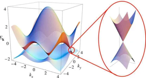
Figure 2-3 - Electronic dispersion of graphene. The conduction band and the valence band touch each other at K
and K’ points. The zoom shows that the dispersion relation close to these points resembles the energy spectrum of
massless Dirac particles. Reproduced from [26].
The band structure nearby the K and K' points has a linear dispersion behavior, as highlighted in the inset of Figure 2-3. In this region, the dynamics of the charge carriers is governed by a Hamiltonian which is very similar to the Dirac Hamiltonian (massless). In fact, charge carriers located around the K and K’ points behave as relativistic particles, whose energy dispersion is given by [26]:
= ±ℏ | | = ±ℏ √ + eq. 2-11
2.1.3
Graphene Production
7 graphene properties can be effectively integrated into modern products. At present, dozens of methods to achieve large-scale production of defect-free graphene are being investigated; some of them are depicted in Figure 2-4.
Figure 2-4 - Several methods of mass-production of graphene which allow a wide choice in terms of size, quality
and price for any particular application. Reproduced from [8].
Liquid-phase exfoliation of graphite oxide consists in exposing graphite to a strong oxidizing agent which promotes the increase of the interplanar space between the graphite layers. A prolonged ultrasonically treatment is then employed to aid graphite to splits into layers, thereby yielding a significant fraction of monolayer flakes in suspension. The reduction of the obtained graphene oxide pellets to its parent graphene state can be achieved by either thermal or chemical approaches. Some of these methods may yield very high quality of the reduced graphene oxide (rGO), similar to pristine graphene, but they can demand the use of large quantity of hazardous agents or can be time consuming to carry out. Viable commercial applications based on liquid-phase exfoliation of graphite such as graphene-based paints and inks have already been demonstrated [8].
8 characteristics (face and orientation), however, epitaxial graphene grown on SiC has the critical advantage to be compatible with standard lithography procedures already used by the semiconductor industry. The two major drawbacks of this technique are the cost of the SiC wafers and the high temperatures (above 1000 ºC) needed for the growth of high quality graphene. Nonetheless, investigations had demonstrated that the UHV Si sublimation process can be improved to produce monolayer graphene films with high mobilities, which may find applications within years when the existing high-frequency transistors, based on III–V materials (InGaAs, GaN, etc.), reaches their limit [8].
Another promising technique to produce graphene is based on the chemical vapor deposition of graphene from a gaseous carbon source onto the surface of a metal catalyst. The production of square meters of uniform polycrystalline graphene films has already been achieved via CVD of graphene [9, 10], which is fundamental for many applications. The transfer of the graphene from the metal catalyst to a target substrate is the major drawback of this method, though improvements had been made over the last years [27]. We discuss this method in details in the next sections.
2.2
Crystal Growth
In this section, a brief background of the exiting crystal growth theories is provided and the application of the concepts presented to the graphene case is highlighted.
2.2.1
Chemical Vapor Deposition of Thin Films
9 layer and the rate at which the active species are consumed at the surface of the catalyst. These fluxes are [28]:
𝑎 𝑎 = ℎ − eq. 2-12
𝑎 𝑎 = eq. 2-13
where, 𝑎 𝑎 is the flux of active species through the boundary layer, 𝑎 𝑎
is the flux of consumed active species at surface, ℎ is the mass transport coefficient, is the surface reaction constant, is the concentration of gas in the bulk, and is the concentration of the active species at the surface. At steady state, theses fluxes are equal to each other and to the total flux. The elimination of in eq. 2-12 and eq. 2-13, leads to:
𝑎 𝑎 = 𝑎 𝑎 = 𝑎 = ℎ +ℎ eq. 2-14
The above equation states the existence of three growth regimes: the surface reaction controlled regime, ℎ , the mass transport limited regime, ℎ and the mixed regime, ℎ ~ . Synthesis under atmospheric conditions and relative low temperatures (Figure 2-6) are usually limited by diffusion of the gas molecules through the boundary layer as transport reactions occur much more slowly than surface reactions due to the Arrhenius dependence of the later (ℎ ). This essentially leads to gas phase reactions in the bulk gas
flow, which are often associated with thickness nonuniformity of the as grown films. This occurs because a small variation in the thickness of the boundary layer can induce a variation in the amount of active species that are diffusing through it.
10
Figure 2-5. Schematic representation of the fundamental transport and reaction steps underlying CVD. Since no
dissolution of carbon is considered, this model can be only applied to metals with low carbon solubility such as
Cu or for lower temperature CVD in which carbon solubility is also insignificant. Reproduced from [30].
Figure 2-6 - Deposition rate as a function of temperature. Reproduced from [31].
Surface reaction limited regime can be achieved by lowering the pressure of the CVD reactor. At low pressures, the flux of active species is lower, essentially leading to fewer
collisions and a higher diffusivity coefficient in the gas phase, Dg,
∝ 𝑃; ℎ = ; eq. 2-15
where P is the total pressure and δ is the boundary layer thickness. Both the diffusivity (Dg) and
11 appropriate synthesis conditions, the diffusion through the boundary layer is enhanced, and it is no longer the rate limiting step (ℎ ). As a result, the growth is limited by surface reactions which generally lead to better film uniformity as long as the temperature is held uniform across the substrate.
Graphene synthesis under atmospheric pressure conditions using Cu foils as catalyst usually leads to monolayer graphene at low methane partial pressures and to multilayer domains at higher methane partial pressures. [12, 13] Low pressure CVD in contrast, normally yields monolayer graphene that is uniform over large areas, and is nearly independent of methane partial pressure. [12, 14, 15] This suggests that graphene growth mechanism is kinetic controlled at the surface and self-limiting under low pressure conditions.
2.2.2
Crystal Growth Theories
Under appropriated synthesis conditions, graphene growth is governed by surface dynamics and can be viewed in the framework of existing crystallization theories. Here we discuss the several crystal growth theories that had been put forward over the years, emphasizing the application of their fundamental concepts to the 2D case of graphene. This provides a useful insight regarding the mechanisms and the kinetics related to the graphene growth.
2.2.2.1 Surface Energy Theory
The conglomeration of atoms which give rise the formation of the first sub-microscopic nucleus of the solid crystal is triggered by fluctuations within the precursor supersaturation (or solution supercooling) in a process known as nucleation (Figure 2-7). The probability of such small clusters grow to form a stable nucleus depends on the temperature, degree of supersaturation and change in free energy associated with its formation. The growth of stable nucleus leads to the formation of a crystal. The microscopic conditions of the growing surface, such as surface discontinues, have a critical effect over the evolution of the growing crystal as showed by Kossel and others [32, 33, 34]. However, the first theories of heterogeneous nucleation treated the formation of stable nuclei on flat surfaces from the thermodynamic point of view.
12 volume. This concept was originally introduced by Gibbs [35] who believed that crystal growth was governed by the same mechanism responsible for the formation of water droplets in mist. Wulff [36] extended Gibbs’s ideas by proposing that anisotropic growth rates could be related to the different surface free energies at the different faces of a growing crystal, i.e the equilibrium shape of a crystal is the one which minimizes the function:
∆ = ∑ 𝐴 eq. 2-16
where 𝐴 is the area of the i-th plane with an interfacial energy of . The interfacial energy or surface energy gives a measure of the disorder of intermolecular bonds at a given surface. Since depends on the crystallography of the growing crystal, it can be very low for some crystal planes, making faceting energetically favored. The surface constructed from the inner envelope of planes perpendicular to the vector is known as Wulff construction and gives the equilibrium shape of the given crystal as illustrated in Figure 2-8.
Figure 2-7. Nucleation and growth mechanism of graphene on Cu. The decomposition of methane leads to
supersaturation of carbon adspecies at the Cu surface. When ccu reaches a critical supersaturation point (cnuc)
13
carbon species are consumed (iii) or until the domains merge together full covering the surface of Cu (iv).
Reproduced from reference [37]
In general, the Wulff construction provide a good agreement with the experimentally observed crystal shapes as long as the growth occurs near to equilibrium, with the attachment of adatoms at the edge of the growing island being the limiting step. Indeed, it was experimentally observed (see section 2.4.3.1) that atmospheric pressure and low carbon feedstock concentration yields regular hexagonal graphene with edges dominated by the zigzag direction in accordance with Wulff theory. The reason for that is the uneven attachment of the diffusive carbon adspecies at graphene’s armchair and zigzag edges. As armchair edges have a higher density of unterminated carbon atoms (4.7 nm-1) than the zigzag edges (4.1 nm-1), it is expected that the former grows faster than the latter, resulting in the conversion of all armchair edges to zigzag by the attachment of new carbon atoms [38].
Figure 2-8 - Surface free energy plotted as a function of the angle θ describing the normal directions to the {hkl}
planes in the Wulff construction. The equilibrium shape of the crystal is given by the dash-dotted curve.
Reproduced from [39].
2.2.2.2 Surface Nucleation Model
14 uninterruptedly until the whole layer is completed. The rate of this advance is proportional to the adatom supersaturation, , and to the mean surface diffusion distance, 𝑥 , [40]:
= ∙ ∙ 𝑥 ∙ ∙ 𝑥 (− 𝑎) eq. 2-17
where is a frequency factor and 𝑎 is the total evaporation energy. The migration distance 𝑥 of an adsorbed atom is given by 𝑥 = 𝜏𝑎where is the surface diffusion coefficient and 𝜏𝑎 is the mean life time of an adantom.
Figure 2-9 - The various atomic positions in the KVS model.
Burton, Cabrera and Frank [41] systematically studied this stepwise stacking, emphasizing the role of screw dislocations as continuous sources of steps on the surface of the crystal. The so called BCF theory views systems as composed of a staircase of terraces, wherein adatoms diffuse until they encounter a step along which they continue to diffuse until they are assimilated by a kink site. On terraces, the local mass conservation of mobile atoms leads to:
= ∇ + − 𝜏 eq. 2-18
where Dis the diffusion coefficient of mobile atoms adsorbed on terraces, c is their surface concentration, F is the incoming flux, and 𝜏 is the typical adatom desorption time. Since adatom
concentration in the vicinity of steps is not equal to the equilibrium concentration under nonequilibrium growth conditions, the diffusion mass flux arriving at the steps defines the boundary conditions for eq. 2-18. Thus, by denoting the upper and lower sides of a step by ±, the equation for the flux of adatoms coming from the upper and lower terraces are respectively given by [42]:
15
+= ( +) = 𝑣+( +− ∗ ) + 𝑣 +− − eq. 2-20
where ± denote the adatom concentration on the lower and upper terraces Figure 2-10 (a) and
∗ refers to the local equilibrium concentration. The attachment-detachment kinetics of
adatoms to the step edge is governed by the kinetic coefficients, 𝑣± (Figure 2-10 (b)), whilst the direct exchange of adatoms between terraces is related to the transparency coefficient, 𝑣 (step crossing probability).
(a) (b)
Figure 2-10 – Vicinal surface considered in BCF theory. (a) The values ± are the adatom densities on the right
(+) and left (−) sides of the step; (b) Kinetic mechanisms governing the growth; D is the diffusion constant, F is
the deposition flux, 𝜏 is the desorption time, and 𝑣± are step attachment coefficients from the lower and upper sides, respectively. Reproduced from [43, 44].
The equilibrium concentration, ∗ , has the Arrhenius form:
∗ = 𝑥 ⁄
eq. 2-21
where is the reference equilibrium concentration and is the chemical potential. The later depends of the step curvature, 𝜅, and of the step stiffnes, ̃ = + ′′, where is the free energy per step length. Thus, the chemical potential can be expressed by:
= Ω̃𝜅 eq. 2-22
16
∗ = + 𝛤𝜅 eq. 2-23
where the constant 𝛤 gives a measure of the edge energy of the step. The growth velocity can be obtained by considering the total flux of adatoms arriving at a step:
v
Ω = = + + −
= ( +) − ( −)
= 𝑣+[ +− + 𝛤𝜅 ] + 𝑣−[ −− + 𝛤𝜅 ] eq. 2-24
The parameters 𝑣± and 𝑣 determines the nature of the growth. When steps are perfectly permeable, 𝑣 → ∞, and + = − = + 𝛤𝜅 + v Ω 𝑣⁄ ++ 𝑣− . The critical consequence of this condition is that atoms may diffuse through many steps before they are incorporated to the crystal lattice, thereby making step dynamics non-local on stepped surfaces. This boundary condition is often used for solidification fronts and was invoked by Meca et al. [22] to describe the “epitaxial” growth of graphene on copper foils (Figure 2-11).
Figure 2-11 – Graphene nuclei shapes obtained on different copper facets and the corresponding shapes obtained
from simulations using the BFC model. In this work was considered the anisotropic diffusion of carbon atoms
induced by the crystallinity of the underlying substrate and the anisotropy of carbon attachment at the graphene
edge. Reproduced from [22].
Another important effect arises when completely asymmetric boundary conditions, 𝑣 → , 𝑣+ → ∞, 𝑣− → , are assumed. The so-called Ehrlich–Schwoebel effect accounts for
17 energy barrier, ΔEES, to descend to the lower terrace. This is because an atom crossing a step
edge passes through an area with a low number of nearest neighbors. These boundary conditions is known as “one sided-model” and is frequently used to describe the step flow (or step motion) induced on vicinal surfaces heated to high temperatures under ultrahigh vacuum conditions (UHV). In this regime, the sublimation of the surface atoms result in macroscopic mass fluxes which leads to surface morphological transitions such as mound formation and step bunching (Figure 2-12). In chapter 4, we invoke these concepts to model the growth of graphene at high temperatures and under LPCVD conditions.
(a) (b) (c)
Figure 2-12 – (a) AFM image of a screw dislocation during the growth of an insulin crystal; (b) STM image of
Si(111) surface showing three macrosteps formed from bunching of many monatomic steps; (c) Hole created on
Si by a lithographic process and filled in after a annealing step at 1300ºC. The 3-fold crystallographic symmetry
of the substrate is expressed in the pattern of steps generated around the filled hole. Reproduced from [42, 45]
2.2.2.3 Reaction Rate Theory
18
τ𝑎 = 𝑣− exp 𝑎/ eq. 2-25
where is the substrate temperature, 𝑣 is the surface vibration frequency and 𝑎 is the re-evaporation energy. Similarly, one can assign characteristic times for the adatom diffusion and for the binding rate between individual atoms and small i-clusters. The characteristic parameters of each material together with the independent experimental variables (P and ) are essential to describe the nucleation and growth at the early stages.
As an example, the growth of graphene on Ru(0001) was explored by Zangwill and Vvedensky [47] using a simple rate model based on the experiments of Loginova et al. [48]. Starting from the assumption that precursor atoms arrive at the substrate at a rate R and stay in a state of mobile adsorption characterized by a life time τa and a diffusion constant D, the
authors of this work stated that migrating adatoms attach directly to the edges of an existing islands or combine with other adatoms forming mobile clusters. In the latter case, clusters composed of = atoms [48] diffuse across the surface with a diffusion constant D' until =
of them combine yielding an immobile island of size i×j [49, 50]. Islands such that continue to grow predominantly by the incorporation of 5-atoms clusters, albeit adatoms attachment at island edges cannot be completely ignored. The rate equations for these kinetic steps are expressed in terms of the homogeneous densities of adatoms n, 5-atoms clusters , and islands
N as [47]:
= − + − 𝑁 + ′
𝑁 − 𝜏𝑎
eq. 2-26
= − − ′ 𝑁 − ′ eq. 2-27
𝑁
= ′ eq. 2-28
19 decrease due cluster dissociation (at rate ), cluster incorporation at island edges (at rate
′ 𝑁), and clusters combination (at rate ′ ). The density of islands (N) in eq. 2-28 increases
by the combination of 5-atoms clusters as discussed before.
The parameters D, D', K and K' have the Arrhenius form previously discussed (eq. 2-25). This set of rate equations retains enough physical content to enable the modeling of a realistic growth process as depicted in Figure 2-13.
Figure 2-13. Carbon adatom density modeled using rate equations (black curve) compared with the corresponding
LEEM data of Loginova et al. [48](red data points). Reproduced from [47].
2.3
Precursor Catalysis
2.3.1
General Aspects of the Catalytic Mechanism
20 transition metals (Co, Ru, Ir, etc.) that have high carbon solubility it has been demonstrated that hydrocarbon decomposes and carbon atoms dissolve into the metal film to form a solid solution. In this case, CVD growth of graphene occurs by carbon bulk diffusion and precipitation during the cooling step [52].
It is highly desirable to understand the underlying atomic details of the precursor pyrolysis in hope to optimize graphene growth conditions. Unfortunately, this knowledge is still very limited, and even the most fundamental question, what the active surface species is at the initial stage of growth, remains unclear. Nevertheless, several attempts had been made to explain the reaction mechanism as discussed by Muñoz and Gómez-Aleixandre in reference [29]. A model based on spectroscopic ellipsometry (SE) experiments [53] and theoretical calculations [54, 55] is schematized in Figure 2-14.
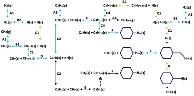
Figure 2-14 - Reaction mechanisms in CVD graphene. The blue arrows indicate the more probable (but not unique)
reaction mechanisms. Reaction of type A: adsorption-desorption. B: dehydrogenation-hydrogenation. C: surface
diffusion or migration (more favorable for dimers C2). D: dimerization with or without simultaneous
dehydrogenation (Dimers with hydrogen are not stable at high temperatures). E: polymerization - (cracking)
decomposition. F: aromatization – decomposition. G: decomposition of aromatics. The green arrows indicate
reactions with hydrogen. Reproduced from reference [29].
21 of the H2 molecules at the bare metal surface also occurs (Reaction B2), thus for metals that exhibit high hydrogen solubility, such as Cu, the surface is expected to be saturated by hydrogen [53, 56], whereas the recombination and desorption of the hydrogen atoms is more likely to occur at metal surfaces which show low hydrogen solubility, such as Ni (Reactions B2, A1). Therefore, in the case of Cu, the hydrocarbon molecules which are introduced in the subsequent step should face a surface partially covered with atomic hydrogen. The resulting competitive mechanisms between the dissociative chemisorption of H2 (reactions A1-B2) and the physical adsorption and dehydrogenation of CH4 (reactions A2-B1) on the metal surface is outlined in Figure 2-14.
According to theoretical calculations [54, 57], dehydrogenation reactions of methane into CHx radicals possibly take place up to x = 2, with CH monomer dissociation being the rate-limiting step in case of Cu catalyst. Molecular dimers are formed by the binding of two of CH compounds in a reaction which is possibly accompanied by simultaneous dehydrogenation (Reaction D). Indeed, it was suggested [55] that C-C dimers are stable on all sites of Cu surface whereas carbon dimers containing hydrogen are very unfavorable on surfaces with low adsorption energies, desorbing or decomposing even at very low temperatures, as experimentally demonstrated [58]. Hence, in the case of Cu, the product of reaction D (Figure 2-14), C2Hz with z = 0, must be considered the most probable end for the dehydrogenation cycle, signaling the formation of C-C bonds with sp2-hybridization. In contrast, complete monomer dehydrogenation and carbon bulk diffusion can be expected in the case of high-solubility metals such Ni.
22 The size of the stable nuclei is subject of controversy. Despite the lack of direct
experimental measurements of the cluster’s atomic structure, Ab initio calculations indicate that
shell structured C21 is a very stable cluster over Rh(111), Ru(0001), Ni(111) and Cu(111) [61]. Nevertheless, once nucleated the growth of a stable island must proceeds by the attachment of carbon species onto graphene edges. Theoretical analysis of graphene-edge reconstruction showed that C insertion into the front of a growing graphene nucleated on Cu (111) should occur preferentially (but not exclusively) in the form of dimers to armchair (AC) edges [62]. Other possibility was raised by Loginova et al. [48] who monitor the evolution of the density of carbon adatoms on Ru(0001) using the reflectivity of low energy electrons. According to these authors, graphene islands must grow mainly by the addition of 5-carbon atoms clusters instead of the standard monomer attachment. This conclusion was derived from the results described in section 2.4.2.
2.3.2
Activation Energy of Precursor Decomposition
Various gas, liquid, and solid precursors (C- and H-based compounds) have been used for graphene synthesis [63, 64, 65]. Zhancheng Li et al. [66] studied the mechanisms of graphene growth related with different carbon sources by dividing the CVD process into three stages. At stage I, precursor molecules collide with the surface, adsorbing on it, or scattering back to the gas phase. If they adsorb, stage II takes place and carbon source molecules dehydrogenate or partially dehydrogenate, forming active surface species which coalesce, nucleate, and grow to graphene at the stage III.
23
2.4
Graphene Growth on Metal Surfaces
The ability of transition metals to provide low activation energy pathways for reactions resides in the fact that their outermost d orbitals are incompletely filled with electrons. This makes transition metals prime candidates for catalysis since they can easily give and take electrons, either by the facile change of oxidation states or by the formation of intermediate compounds.
Graphene CVD was first reported on Ni and Cu substrates [52, 68], then followed by intense research activities and publications using a variety of other transition metal substrates such as Ru and Ir [69], Pd [70] and Pt [71]. Hereafter, we will discuss the general aspects related to the graphene CVD on metal substrates.
2.4.1
Graphene Growth on Ni
24
Figure 2-15. Schematic diagrams of graphene growth mechanism on Ni(111) (a) and polycrystalline Ni surface
(d). Optical image of graphene grown on Ni(111) (b) and polycrystalline Ni (e). Maps of I2D/IG of Raman spectra
collected on the Ni(111) surface (c) and on the polycrystalline Ni surface (f). Reproduced from reference [73]
Other important aspect of CVD graphene on Ni is that the thickness and quality of the films are strongly affected by the carbon segregation process, which ultimately depends on the cooling rate. Medium cooling rates are found to lead to optimal carbon segregation and produce continuous few layer graphene. The specific growth parameters used by several groups are summarized in Table 1 reproduced from ref. [73].
2.4.2
Graphene growth on Ru
25 active surface species driving graphene domain growth is 5-C clusters [48]. This supposition was made by noting that the growth velocity of the graphene front, 𝑣, is a highly nonlinear function of the supersaturation. Indeed, the adjust of the experimental curves of Graphene
Growth rate vs. C monomer coverage shown in Figure 2-16(a) leads to:
𝑣 = [( ⁄ ) − ] eq. 2-29
where is the carbon adatoms density and is its equilibrium density.
In addition, it was demonstrated that graphene first nucleates at step edges, which are believed to lower the barrier to graphene nucleation. However, as the C monomer concentration increases, multiple nucleation events take place at the terraces of the Ru substrate, as depicted in Figure 2-16(b).
(a) (b)
Figure 2-16 – (a) Island growth rate as function of monomer concentration; (b) Time evolution of C monomer
concentration during C deposition. Nucleation start to occur at the steps edges of Ru substrate, and then it takes
place at the Ru terraces at higher C concentrations. Reproduced from [48].
26 the uncovered parts of Ru surface, crossing the typical distribution of terraces and monatomic steps of single crystal metal surfaces. At lower pressures or higher temperatures, however, it was observed that graphene no longer traverses the atomic steps, but continues growing on the same terrace level, i.e. together with the Ru terrace. According to the authors, this can only mean that Ru atoms are transported to the growing step edge where they enter underneath the graphene layer. Both growth modes are presented in Figure 2-17. This work provides a noteworthy evidence of the influence of the substrate dynamics during the graphene growth.
Figure 2-17 - In situ STM scans showing: (a-b) the growth of graphene (blue) across the steps of the Ru(0001)
surface (orange) at 665º C; (c-d) graphene growth at higher temperatures (or low pressures) accompanied by the
extension of the underneath Ru terrace. e) Extensive faceting of the Ru surface induced by the above graphene
layer. Reproduced from [74].
2.4.3
Graphene growth on Cu
27
2.4.3.1 Atmospheric pressure CVD – APCVD
The controlling and characterization of single-crystal graphene grains, prior to the coalescence of a complete monolayer, was the subject of the work of Qingkai Yu et al. [12]. In their study, carried out at 1050 ºC under atmospheric pressure of a gas mixture of CH4 diluted in Ar (concentration 8 ppm) and H2, they synthesized hexagonally shaped single-crystal grains. They found that the junction formed between coalescing domains deteriorate the electrical transport, even when the edges of the individual graphene domains were aligned and parallel to zigzag directions. Moreover, it was shown that graphene grains do not have well-defined epitaxial relationship with the Cu substrate and that spatially ordered arrays of graphene domains can be artificially initiated by pre-patterned growth seeds, as shown in Figure 2-18.
Figure 2-18. (a-c) SEM image showing an array of seed crystals patterned on Cu foil by e-beam lithography. (d)
SEM image of a seeded array of graphene domains next to a randomly-nucleated set of graphene domains in an
area without seeds. Scale bars in (a-c) are 10 µm and the scale bar in (d) is 200 µm. Reproduced from [12].
28 growth progresses, the feeding flow is then increased to provide continuous growth for the graphene domains. It was demonstrated that through this process the nucleation density of graphene domains can be lower as ~100 nuclei/cm2 and the dimension of single crystal grain up to ~1.2 mm. According to the authors, the electro-polishing of the Cu substrate, followed by a long thermal pre-treatment, is also an important step for the growth of these large graphene domains.
Figure 2-19. (a) APCVD growth of graphene at 1050 °C with a linear increase of temperature of the polystyrene
source and total reactant gas flow. (b-d) SEM image of the obtained hexagon-shaped graphene domains.
Reproduced from [65].
The morphological evolution of graphene crystals in atmospheric pressure CVD on ultra-smooth, epitaxial Cu(100), Cu(110), and Cu(111) thin films, was also investigated. The growth of large graphene domains at low density was achieved on the inside of an enclosure formed by bending a thick copper foil to form an envelope [9]. It was speculated that the inside of the enclosure offers a much lower partial pressure of methane and a “better” environment during growth, providing a much lower pressure of unwanted species and a quasi-static background of Cu vapor.
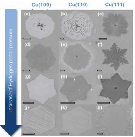
29 of the growth species around the nucleus perimeter; (d) anisotropic hydrogen etching of graphene domains.
Moreover, the trend displayed in Figure 2-20 suggests that hydrogen shifts the growth kinetics from edge-attachment-limited to diffusion-limited. In other words, if the attachment of carbon at graphene edge is the fastest reaction, the growth of graphene nuclei will be limited by the rate at which diffusive carbon adspecies reach the graphene border. This growth mode is much more common during LPCVD process, which is discussed in the next section.
Figure 2-20. Graphene island morphology dependence on H2:CH4 in APCVD. First, second, and third columns
represent the island structure on Cu(100), Cu(110), and Cu(111). Reproduced from [16].
2.4.3.2 Low pressure CVD – LPCVD
30 𝜋 − ⁄ P. In the particular case of graphene synthesis, it was additionally found a
relationship between the grown graphene and the underneath substrate crystallography.
Wood et al. [17], combining electron backscatter diffraction with spatial Raman techniques, studied the effects of polycrystalline Cu on graphene growth. They verified that Cu(100) surfaces often causes slow growth of multilayer graphene, whereas high index Cu facets frequently induces fast growth of compact graphene islands with anisotropic lobed shapes. On the other hand, Cu (111) surface was found to promote fast growth of monolayer graphene with few defects. They concluded that the growth mechanism of graphene was crystallographically dominated, strongly depending on the surface energy of the Cu crystal structure and little affected by the surface roughness. These results triggered the attention of other research groups for the largely neglected influence of the Cu substrate in graphene nucleation and growth.
Zang et al. [14] reported the growth of large-grain, single-crystalline graphene flowers
with grain size up to 100 μm using a vapor trapping LPCVD method. Controlled growth of graphene flowers with four lobes and six lobes had been achieved by varying the growth pressure and the methane to hydrogen ratio. However, electron backscatter diffraction characterization revealed that the graphene morphology had little correlation with the crystalline orientation of the underlying copper substrate. According to the authors, graphene morphology mostly relates to the local environment around the growth area (i.e. temperature, total pressure and H2:CH4 ratio) rather than the crystalline structure of the underneath copper crystal.
Contradicting the study mentioned above, Wofford et al. [20] showed that 4-fold-symmetric graphene islands nucleate and grow preferentially on the Cu (100)-textured surface, though each of the four lobes of these graphene domains had a different crystallographic alignment with respect the underlying Cu. According to the authors, this well-ordered
31
Figure 2-21. Bright (a) and dark field (b-e) LEEM images showing the spatial distribution of lobes of
4-fold-symmetric graphene islands nucleated on Cu(100). Copper step edge accumulation (hillock formation) is
illustrated in (f-i). Reproduced from [20].
The complex interplay between graphene and the underneath substrate was also subject of others studies [22, 16] where shape, orientation, edge geometry, and thickness of the graphene domains were found to be controlled by the crystallographic orientations of Cu substrates. In fact, it was demonstrated that flower-like graphene islands develop dendritic branches which extend hundreds of microns in the , and directions on Cu(100), Cu(110), and Cu(111), respectively. Jacobberger and Arnold [16] attributed this phenomenon to the development of Mullins-Sekerka morphological instabilities [75] during the growth. Meca et al. [22], on the other hand, relate the morphological evolution of the graphene islands to the anisotropic diffusion of carbon atoms induced by the crystallinity of the underlying substrate and to the anisotropy of carbon attachment at the graphene edges (see Figure 2-11).
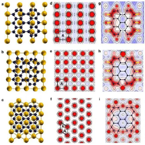
32 computational modelling, the authors calculate the most stable position at which a nanoscale nucleating domain (C28) may preferentially locate above each Cu surface. Their results are shown in Figure 2-23.
Figure 2-22. (a-d) Shape and orientation dependence of LPCVD graphene domains on polycrystalline Cu. (e,f,g,h)
SEM images of representative LPCVD graphene domain shapes grown on Cu{101}, Cu{001}, Cu{103}, and
orientations close to Cu{111}, e.g., Cu{769}, respectively.
According to Figure 2-23(a-b), the graphene C28 cluster is stabilized on Cu surfaces (101) and (001) when its dangling bonds at the zigzag edge form directional bonds with the Cu surface atoms along the directions. On Cu(111), however, the C28 become stable when its atoms at the zigzag edge hybridize with two neighboring Cu surface atoms as depicted in Figure 2-23 (c). In all these cases, the armchair edge atoms hybridize mainly among themselves, enhancing electron density near the corner of the C28 cluster (Figure 2-23-(g-i)) and promoting the growth in the [-101] direction.
33 the growth conditions and/or crystallographic orientations of the substrate. Atmospheric pressure CVD, meanwhile, generally led to graphene domains of six-fold-symmetric hexagons.
Figure 2-23. Computational modeling of graphene clusters on Cu{101}, Cu{001}, and Cu{111}. Red circles
correspond to the surface atoms (high electron density), while regions with depleted electron density are equivalent
to available adatomsites (labeled A). Strong one-to-one hybridization occurs along the Cu direction between
the electron orbitals of the zigzag edge atoms of C28 and Cu surface atoms on Cu(101) and Cu(001) indicated by
yellow lines in g and h. Weaker one-to-two atom bonding between one C and two Cu atoms is observed on
34
3
Experimental Setup and
Characterization Tools
3.1
CVD Reactor
All graphene growth experiments presented in this thesis were carried out in a cold-wall reactor which operates under high vacuum conditions. I actively participated in the construction project, being responsible for all assembly and initial testing, as well as the project of complementary components. Services of welding and fabrication of parts such as ducts and connections were made in the machine shop of the physics department of UFMG.
The system consists of a cylindrical stainless steel chamber (SS316) with an internal diameter of 250 mm and height of 300 mm. It is connected to a turbo-molecular pump (Edwards HFA 301/451), which in turn is connected to a mechanical rotary pump (Edwards RV12). Note, however, that although the pumps are connected in series, the chamber can be pumped directly by the mechanical rotary pump as depicted in the diagram of Figure 3-1. This allows one to operate in low vacuum, 10-3 Torr, which is pretty much the ultimate limit of the mechanical pump. Naturally, when the mechanical pump is connected directly to the chamber, the turbo-molecular pump is isolated from the system by a Gate valve coupled to a cf flange 4-1/2''. This operation is done manually.
35 The pressure is monitored at the outlet of the turbo-molecular pump by a Pirani pressure gauge, and inside the chamber by another Pirani, and by a cold cathode gauge, which are connected as diagrammed in Figure 3-1(in red). Operating in high vacuum, with the two pumps working in series, it is possible to achieve pressures below × − Torr in a short period of time (~ 30 min).
Inside the chamber, a resistive heater is suspended by two copper cylinders which are attached to an electrical feedthrough installed on a cf flange at the base of the chamber. Apart from serving as support for the heater, the copper pieces are also used to transfer the electrical power from an AC voltage source (which is connected to a voltage transformer) through the vacuum system wall, to the electrodes (carbon screws) connecting the heater (Figure 3-2)
Originally, the CVD reactor was put in operation using a commercial resistive heater made of pyrolytic graphite covered with pyrolytic boron nitride (Boralectric® Sample Heater, purchased from Tectra, Germany). However, after few months of usage, the heating element stoped working due the degradation of pyrolytic graphite in the contact. The perspective of the long waiting time that would be necessary to import another component encouraged us to produce our own heater. To this end, we carved in a graphite bar a very thin region which came to be the ohmic heater displayed in Figure 3-2 (b). The working area of this resistive circuit is 1 cm2 and its thickness is approximately 0.5 mm. It can achieve temperatures up to 1300 ºC with currents near to 90 A. The effects of heat transfer by irradiation on sensors and connectors are attenuated by two concentric heat shields (confectioned in tantalum) surrounding the base of the heater. Air coolers are positioned on the outer walls of the chamber to help cool the system.
36
Figure 3-2 – (a) Commercial sample heater; (b) Homemade graphite heater.
Gaseous reactants are admitted into the reactor via a gas feedthrough connected to a gas mixer which is coupled to mass flow controllers (M100B MASS-FLO®) through a pipeline. Flow controllers for the gases methane, hydrogen and argon are currently installed, but a small change in the gas line allows the replacement of methane by ethylene. A photograph of the complete system is shown in Figure 3-3.
Figure 3-3 – Photography of the system built for graphene chemical vapor deposition.
Copper foils were placed on the heater mounted inside the chamber in order to serve as metal catalyst and substrate in the chemical vapor deposition of graphene. The growth routine and parameters sets are discussed in details in the following sections. However, it is worth to mention here that during the growth, graphene domains nucleated on the Cu surface and merge together to form a uniform graphene sheet as depicted in Figure 3-4. One can investigate either the film proprieties as well as graphene single-domains characteristics (before full surface coverage) by controlling the synthesis time. Both studies are presented in the next sections.
37
Figure 3-4 – Formation of a continuous graphene film by coalescence of monocrystalline domains of graphene.
3.2
Optical Microscopy Characterizations
Optical microscopy was employed to characterize the as-grown graphene immediately after the CVD growth. The major advantage of this technique is the possibility to access critical features of the grown graphene, such as grain size and morphology, in a fraction of the time usually demanded by other imaging methods (e.g. scanning electron microscopy).
The selective oxidizing of the underlying copper through thermal annealing in air enable the acquisition of high quality optical images of graphene grain boundaries as well as separated domains directly on the metal substrate, without the necessity to transfer the grown graphene to a Si/SiO2 substrate. The reason for that is the increase of the interference color contrast between Cu and Cu oxide produced by the oxidation of the Cu regions uncovered with graphene (Figure 3-4).

![Figure 2-6 - Deposition rate as a function of temperature. Reproduced from [31].](https://thumb-eu.123doks.com/thumbv2/123dok_br/14990809.11200/23.892.267.659.560.865/figure-deposition-rate-function-temperature-reproduced.webp)