Graphene to graphite: electronic changes within DFT calculations
A.Z. AlZahrani and G.P. SrivastavaSchool of Physics, University of Exeter, Stocker Road, Exeter EX4 4QL, U.K.
(Received on 22 August, 2009)
Calculations based on the first-principles pseudopotential plane-wave method and density-functional theory are performed to investigate the electronic properties of graphene, bilayer graphene, multilayer graphene, and graphite. From an analysis of the electronic band structure close to the Fermi level, we have quantified the gradual change in the Fermi surface topology from the point-like structure for graphene to a warped triangular shape for graphite. We have also discussed the gradual change in the electron and hole effective masses and velocities as the system evolves from graphene to graphite.
Keywords: Graphene; Bilayer graphene; Multilayer graphene; Graphite; Density functional theory; Local density approxima-tion; Pseudopotential theory; Fermi surface; Electronic structure
I. INTRODUCTION
Recently, carbon-based materials such as graphene (a sin-gle hexagonal layer of carbon atoms) and graphite (three-dimensional hexagonal structure of carbon atoms) have gen-erated a lot of interest due to their exotic electronic properties [1, 2]. From the electronic structure point of view, mono-layer graphene has a linear band dispersion near the corner (K) point of its Brillouin zone originating from the π and π∗bondings between the two carbon basis atoms within the
hexagonal unit cell. This results in carriers (electrons and holes) to behave like massless Dirac particles with very large Fermi velocity [3]. The carrier mass and velocity are found to change strongly with the increase in the number of atomic layers in a graphene sample [3]. The basic understanding of the electronic band structure and the Fermi surface topol-ogy of graphite has been gained for a long time [4–8]. Mc-Clure [5] has described the energy band structure of graphite close to the Fermi level using the Slonczewski-Weiss model. This work has revealed that the electron and hole Fermi surfaces are highly elongated and aligned along the high-symmetry edges of the Brillouin zone. The band structure calculations obtained by Zunger [7] have shown that the elec-trons are confined to narrow holes close to the Brillouin zone edges. Moreover, Tatar and Rabii [8] have reported that the constant-energy Fermi surfaces of graphite show clear sym-metry of the bands above and below the Fermi level.
Despite these basic understandings, an important area that has not been investigated thoroughly is the change in the key electronic parameters, such as carrier effective mass, carrier velocity, and Fermi surface topology, as the system evolves from the strictly two-dimensional (sp2) graphene structure to
the three-dimensional (sp2+pz) graphite structure. For a full
understanding of the origin of these changes, it is of particu-lar importance to thoroughly investigate the basic electronic structure such as the dispersion of the band structure near the high-symmetry edges (such as K and H points) and the Fermi surface at these particular points.
In this paper, we present a first-principles theoretical in-vestigation of the electronic band structure of graphene, bi-layer graphene, multibi-layer graphene, and graphite. From these calculations, the effective masses and velocities of the carriers have been estimated, and compared with available experimental measurements, for each of these structures. An attempt has been made to explain the gradual change in
the electronic properties from the two-dimensional graphene structure to the three-dimensional graphite structure.
II. COMPUTATIONAL METHOD
We have performed first-principles calculations within the density functional theory [9] using the local density approximation (DFT-LDA). The Perdew-Zunger exchange-correlation scheme [10] was considered to treat the electron-electron interaction. The electron-electron-ion interaction was treated by using the ultrasoft pseudopotential for carbon [11]. The single-particle Kohn-Sham [12] wave functions were ex-panded in the framework of a plane wave basis set with a kinetic energy cutoff of 60 Ryd. Self-consistent solutions of the Kohn-Sham equations were obtained by employing the 14×14×14 and 14×14×4k-points Monkhorst-Pack sets [13] within the Brillouin zones for graphite and other structures, respectively. For Brillouin zone integration the eigenvalues at the specialkpoints were thermally smeared by using the Methfessel-Paxton scheme [14] with a broad-ening factor of 0.00002 Ryd. These parameters have been carefully chosen after several convergence test calculations.
We adopted a supercell technique for modelling the multi-layer graphene. A supercell contained seven atomic multi-layers of carbon atoms and a vacuum region equivalent to eight atomic layers. Relaxed atomic positions were obtained by using the total-energy and force minimisation methods. The equilib-rium atomic positions were determined by relaxing atoms in all except the eighth layer, which was kept in its bulk posi-tion.
III. RESULTS AND DISCUSSION
III.1. Bulk graphite
We made a series of total energy calculations with differ-ent choices of the in-plane lattice constant a and the ratio c/aof the out-of-the plane to the in-plane lattice constants. From our calculations we determined that the minimum en-ergy configuration results for the choicesa=2.448 ˚A and c/a=2.711. These values are in agreement with several previousab initiocalculations [15, 16].
and along the inter-planar direction (the KH direction in the Brillouin zone), is shown Fig. 1(a). Within about 1 eV around the Fermi level we have four electronic bands, two derived fromπorbitals and two from theπ∗orbitals of the
basis atoms. The inner pair of theπ/π∗bands is degenerate and shows very little dispersion along the KH direction in the Brillouin zone. This pair of bands is electron-like and hole-like towards the K and H points, respectively. The width of the electron-like part of the band is very slightly wider than the width of the hole-like part. Also, since the band crosses the Fermi level at approximately KH/3, it indicates that the hole state is more elongated than the electron state. These results are in agreement with previous first-principles works (see, e.g. Ref. [8]). The outer pair of theπ/π∗ bands are
dispersive along the KH direction, with theπandπ∗bands dispersing up and down the energy axis, respectively. Our calculated energy gap between theπandπ∗bands is 0.07 eV at the H point and 1.41 eV at the K point.
K H
−0.75 −0.50 −0.25
0 EF
0.25 0.50 0.75 Electrons Holes Energy (eV) Energy (eV) π π π * * * π π , π
K Γ M
−20 −15 −10 −5 0 5 10 15 20 (b) (a) Experiment Theory K H M Kx Ky Kz Γ
FIG. 1: The band structure plot of (a) bulk graphite along the KH direction and close to the Fermi level and (b) monolayer graphene along the high-symmetry directions (KΓM). The hexagonal Bril-louin zone is also shown.
In Fig. 2(a) we have plotted the in-plane dispersion of the electronic bands near the Fermi level. [We performed cal-culations along several in-plane directions, and found sim-ilar results.] An attempt to fit such curves close to the
K point suggests a purely quadratic behaviour, indicating that the carriers are normal (massive) electrons. From these calculations we estimated the effective electron mass value m∗=0.043m
e. This value is consistent with the reported
theoretical value of 0.045me[8, 17] and close enough to the
experimental result of 0.06me [18]. We also calculated the
electron (in-plane) velocity of the magnitude 0.94×10⁶m/s.
This result is in good agreement with the angle-resolved pho-toemission data obtained by Zhouet al. [19] who obtained a value of 0.91×10⁶m/s. When fitting the in-plane disper-sion of hole bands we needed to include both the linear and quadratic terms. This suggests that the behaviour of holes can be described as a mixture of Dirac-like (massless) and normal (massive) particle. Our conclusions regarding the quasi-particle nature of the electrons (as normal) and holes (as a mixture of normal and Dirac-like) near the Fermi level in graphite support the phase analysis of quantum oscilla-tions [20] and the quantum Hall effect [21].
K K K K 0.005 0.005 0.005 0.005 0.01 0.01 0.01 0.01 0.015 0.015 0.015 0.015
Wavevector, k (2/a)
Wavevector, k (2/a) π π
−1.6 −1.55 −1.5 1.3 1.35 1.4 −2.2 1.45 6.98 1.5 −2.18
Energy, (eV) 7
−2.16 7.02 −2.14 7.04 −2.12 7.06 −2.1 Energy, (eV) K K K (b) (d) (a) (c)
FIG. 2: The in-plane electronic band structure for the innermostπ∗ band near the the K point for (a) graphite, (b) monolayer graphene, (c) bilayer graphene, and (d) multilayer (7-layer) graphene. The insets indicate the dispersion curves for the outer pairs of theπ/π∗ bands.
The shape and symmetry of the Fermi surface in graphite has long been a topic of discussion, with contradictory views in the 1950s [22], 1960s [6] and 1970s [23]. First-principles band structure calculations by Tatar and Rabii in 1982 [8] provide the accepted picture for the band structure, and shape and symmetry of the Fermi surface. It should be noted that Tatar and Rabii constructed the Fermi surface by adopting two parametrized fitting procedures of bands. In our work the Fermi surface was mapped without the need for any pa-rameterization of bands. Our calculations have presented re-sults, shown in panel (a) of Figs. 3 and 4, in close agreement with those by Tatar and Rabii. We find that the Fermi surface is elongated along the KH direction. The shape of the Fermi surface can be described as a warped and squeezed cylinder, with almost equal width at the K and H points. The squeezed feature can be seen as a ‘neck’ at KH/3. The warped trian-gular cross-sections at thekz=0 andkz=KH heights can be
(a) (b)
(c) (d)
FIG. 3: Top view of the Fermi surfaces of (a) graphite, (b) mono-layer graphene, (c) bimono-layer graphene, and (d) multimono-layer graphene.
(b)
(d) (a)
(c) K K
H
FIG. 4: Diagrams showing details of the full extent of the Fermi sur-faces, of (a) graphite, (b) monolayer graphene, (b) bilayer graphene, and (d) multilayer graphene.
III.2. Monolayer graphene
The electronic band structure of graphene is shown in Fig. 1(b). Due to only two basis atoms in graphene there is only one pair ofπ/π∗bands, which is degenerate at the K point, coinciding with the Fermi level. This means that this band is partially filled at the K point, and thus is contributed by both electron-like and hole-like states. Figure 2(b) shows that the dispersion of this band on the planar Brillouin zone around the K point (i.e. close to the Fermi level) is entirely linear (Dirac like) for both electrons and holes. The presently computed dispersion curve for theπband agrees very well with the angle-resolved photoemission measurements made by Ohtaet al[24]. The small level of disagreement between theory and experiment with regards to the energy locations at various in-plane wave vectors is well within the error margin of the experimental measurements. Our results are also in very good agreement with the results obtained by Latit and Henrard [25] who used an almost identical theoretical and computational method.
From our calculations of the in-plane dispersion curves slightly above and slightly below the Fermi energy we have estimated velocity results of 1.11×10⁶ m/s and 1.04×10⁶ m/s for electrons and holes, respectively. We attribute the difference between the hole and electron velocities of ap-proximately 6% to the asymmetry of their band states. These results are in excellent agreement with the cyclotron reso-nance study by Deaconet al.[3] who measured the electron velocity of 1.093×10⁶m/s and estimated the hole velocity to be 5% lower than the electron velocity. Our calculated elec-tron velocity is also in excellent agreement with the value of 1.1×10⁶m/s deduced by Jianget al. [26] using infrared
spectroscopic studies.
The Fermi surface for the monolayer graphene is shown in Fig. 3(b). Although the Fermi surface for an ideal graphene sheet has an area of zero size, the finite size of the plotted shape is due to the thermal broadening in the calculations. The resulting shape of the Fermi surface is a triangle centred at the K points in the Brillouin zone. As our calculations have been made using a supercell geometry, the resulting Fermi surface extends normal to the graphene sheet with both ends being triangles of equal dimensions. A clearer picture of the computed shape is shown in Fig. 4(b).
III.3. Bilayer graphene
We have modelled the bilayer graphene using the symmet-ric double layer (i.e. the Bernal, or AB, stacking of graphite) arrangement. Due to a basis of four atoms, there are two pairs of π/π∗ bands. Consistent with previous theoretical works
be-haviour of the dispersion relation is well accepted [2]. From our results we extract the carrier effective mass 0.022meand
velocity 1.10×10⁶m/s. The results from the tunnelling mea-surements done by Liet al. [28] suggest that the velocity of the carriers in bilayer graphene is 1.07×10⁶m/s, which is in fairly good agreement with our results.
The inter-layer interaction in the bilayer graphene re-sults in a noticeable change in the shape of the Fermi sur-face around K, the Brillouin zone edge point. The triangu-lar Fermi surface for the monolayer graphene changes to a hexagonal shape. A detailed side view in Fig. 4(c) suggests that an identical hexagonal shape is maintained for both elec-trons and holes. This is rather different from the results of earlier tight-binding calculations (see, e.g. [2]) which have explained the change in the Fermi surface from the mono-layer to the bimono-layer structure in terms of trigonal distortion (or warping).
III.4. Multilayer graphene
From the electronic band structure calculations for a seven-layer graphene system, we find that there are seven pairs ofπ/π∗bands. The innermostπ/π∗pair is degenerate at the K point, making the system a zero-gap semiconductor. The outer six pairs of theπ/π∗bands are split, with the min-imum and maxmin-imum gaps at K between theπandπ∗bands
being 0.14 eV and 1.45 eV, respectively. The energy gap of 1.45 eV between the outermost pair is close to that for bulk graphite. The splittings of the π andπ∗ bands are due to different amounts of interactions between the various atomic layers.
We further made calculations for the in-plane electronic band structure, close to the K edge of the Brillouin zone. We observe that the in-plane dispersion of the electronic band structure (shown in Fig. 2(d)) is quite similar to the disper-sion in bulk graphite, but with a slightly more curvature close to the K edge. The values of the electron effective mass and velocity for the multilayer graphene are different com-pared with bulk graphite. The effective mass of the multi-layer graphene is reduced by roughly 28%, and the velocity, of 1.0×10⁶m/s, has increased by 6.4%. Our calculated
elec-tron velocity agrees well with value deduced by Sadowski et al. [29] from their observed cyclotron resonance-like and electron-positron-like transitions in infrared transmission ex-periments. As is the case with the bilayer graphene, we could not find any experimental or other theoretical measurements of the electron effective mass for a multilayer graphene to compare or contrast our results with. The Fermi topology for the multilayer graphene shows a warped triangular shape, as shown in panel (d) of Figs. 3 and 4.
III.5. Gradual changes from graphene to graphite
From our work we are able to draw conclusions regarding the gradual development in the electronic properties with the dimensionality change from the two-dimensional graphene to the three-dimensional graphite. Within the energy range ±2.0 eV around the Fermi level, the occupied and
unoccu-pied bands are of the orbital charactersπandπ∗, respectively. The number of the pair ofπ/π∗bands is directly related to the number of basis atoms in the unit cell: e.g. one for graphene, two for bilayer graphene and for bulk graphite, and seven for the seven-layer graphene. For a multilayer graphene there is noticeable splitting in theπandπ∗bands, except for the innermost pair at the K point.
The in-plane electronic band dispersion is Dirac-like for graphene, a mixture of linear and quadratic for bilayer graphene and multilayer graphene, and quadratic for bulk graphite. The electron velocity decreases from the single-layer graphene to the bisingle-layer and multisingle-layer graphene, and further to bulk graphite. The electron effective mass grad-ually increases from the bilayer graphene to multilayer graphene and then to bulk graphite. The shape of the Fermi surface changes as follows: triangle for graphene, hexagonal for bilayer graphene, warped triangle for multi-layer graphene, and more warped triangle for bulk graphite. While the cross-section of the Fermi surface does not change along the KH direction for ideal monolayer graphene, bilayer graphene and multilayer graphene, it has a neck-like feature at the KH/3 point for bulk graphite.
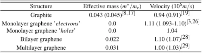
Structure Effective mass (m∗/me) Velocity (106m/s) Graphite 0.043 (0.045)[8,17] 0.94 (0.91)[19] Monolayer graphene ’electrons’ 0.0 1.11 (1.093-1.10)[3,26]
Monolayer graphene ’holes’ 0.0 1.04
Bilayer graphene 0.022 1.10 (1.07)[28] Multilayer graphene 0.031 1.00 (1.03)[29]
TABLE 1: Electron and hole effective masses and velocities in monolayer graphene, bilayer graphene, multilayer graphene, and graphite. Available experimentally measured results are presented
in parentheses.
IV. SUMMARY AND CONCLUSION
We have studied the electronic properties of graphene, bi-layer graphene, multibi-layer graphene, and bulk graphite us-ing the plane-wave pseudopotential method and the den-sity functional theory within the local denden-sity approxima-tion. The shape of the Fermi surface is found to be trian-gle for graphene, hexagonal for bilayer graphene, warped triangle for the multilayer graphene, and more warped tri-angle for bulk graphite. For graphite the cross-section of the Fermi surface has a neck-like feature at the KH/3 point. The in-plane electronic band structure near the zone edge K is Dirac-like for graphene, a mixture of linear and quadratic for bilayer graphene and multilayer graphene, and quadratic for bulk graphite. Our work suggests that the electron mass (ve-locity) gradually increases (decreases) with the thickness of the graphene layer. The electron effective mass is calculated to be 0.022me, 0.031me, and 0.043me for bilayer graphene,
multilayer graphene, and graphite, respectively. The electron and hole velocities in monolayer graphene are 1.11×10⁶and 1.04×10⁶ms−1, respectively. The electron velocity
gradu-ally reduces to 1.10×10⁶, 1.0×10⁶, and 0.94×10⁶ms−1for
systems are in agreement with experimentally measured re-sults.
Acknowledgements
A. AlZahrani gratefully acknowledges financial support from King Abdulaziz University (KAU), Saudi Arabia. The
calculations reported here were performed using the Univer-sity of Exeter’s SGI Altix ICE 8200 supercomputer.
[1] R. J. Nicholas, A. Mainwood, and L. Eaves, Phil. Trans. R. Soc. A366, 189 (2008).
[2] A. H. Castro Neto, F. Guinea, N. M. R. Peres, K. S. Novoselov and A. K. Geim, Rev. Mod. Phys.81, 109 (2009).
[3] R. S. Deacon, K.-C. Chuang, R. J. Nicholas, K. S. Novoselov, and A. K. Geim, Phys. Rev. B76, 081406 (2007).
[4] P. R. Wallace, Phys. Rev.71, 622 (1947). [5] J. W. McClure, Phys. Rev.108, 612 (1957).
[6] S. J. Williamson, S. Foner, and M. S. Dresselhaus, Phys. Rev.
140, A1429 (1965).
[7] A. Zunger, Phys. Rev. B17, 626 (1978).
[8] R. C. Tatar and S. Rabii, Phys. Rev. B25, 4126 (1982). [9] P. Hohenberg and W. Kohn, Phys. Rev.136, B864 (1964). [10] J. P. Perdew and A. Zunger, Phys. Rev. B23, (1981) 5048. [11] D. Vanderbilt, Phys. Rev. B41, 7892 (1990).
[12] W. Kohn and L. Sham, Phys. Rev.140, A1133 (1965). [13] H.J. Monkhorst and J.D. Pack, Phys. Rev. B13, 5189 (1976). [14] M. Methfessel and A. T. Paxton, Phys. Rev. B40, 3616 (1989). [15] M. T. Yin and M. L. Cohen, Phys. Rev. B29, 6996 (1984). [16] M. C. Schabel and J. L. Martins, Phys. Rev. B46, 7185 (1992). [17] F. Rozploch, J. Patyk, and J. Stankowski, Acta. Phys. Pol.112,
557 (2007).
[18] D. E. Soule, IBM J. Res. Dev.8, 268 (1964).
[19] S. Y. Zhou, G.-H. Gweon, J. Graf, A. V. Fedorov, C. D. Spataru, R. D. Diehl, Y. Kopelevich, D.-H. Lee, S. G. Louie, and A. Lanzara, Nat. Phys.2, 595 (2006).
[20] I. A. Luk’yanchuk and Y. Kopelevich, Phys. Rev. Lett. 93, 166402 (2004).
[21] I. A. Luk’yanchuk and Y. Kopelevich, Phys. Rev. Lett. 97, 256801 (2006).
[22] J. C. Slonczewski and P. R. Weiss, Phys. Rev.109, 272 (1958). [23] J. A. Woollam, Phys. Rev. B3, 1148 (1970).
[24] T. Ohta, A. Bostwick, J. L. McChesney, T. Seyller, K. Horn, and E. Rotenberg, Phys. Rev. Lett.98, 206802 (2007). [25] S. Latil and L. Henrard, Phys. Rev. Lett.97, 036803 (2006). [26] Z. Jiang, E. A. Henriksen, L. C. Tung, Y.-J. Wang, M. E.
Schwartz, M. Y. Han, P. Kim, and H. L. Stormer, Phys. Rev. Lett.98, 197403 (2007).
[27] H. Min, B. Sahu, S. K. Banerjee, and A. H. MacDonald, Phys. Rev. B75, 155115 (2007).
[28] G. Li and E. Y. Andrei, Nat. Phys.3, 623 (2007).