juan pablo vasco cano
R E F L E C T I V I T Y C A L C U L AT I O N S I N L3 P H O T O N I C C R Y S TA L S L A B C AV I T I E S
juan pablo vasco cano
adviser
Prof. Dr. Paulo Sergio Soares Guimarães co-adviser
Prof. Dr. Herbert Vinck Posada
Thesis presented to
universidade federal de minas gerais as partial requirement for the title of
master in physics Instituto de Ciências Exatas
Departamento de Física
Juan Pablo Vasco Cano: Reflectivity calculations in L3 photonic crystal
slab cavities,
© January2013 supervisors:
Prof. Dr. Paulo Sergio Soares Guimarães
Departamento de Física Instituto de Ciências Exatas
Universidade Federal de Minas Gerais Belo Horizonte, Brasil
Prof. Dr. Herbert Vinck Posada
Departamento de Física Facultad de ciencias exactas
Universidad Nacional de Colombia Bogotá, Colombia
location:
A B S T R A C T
In this work, a detailed study is made of the reflectivity spectrum of L3photonic crystal slab cavities. The scattering matrix method for patterned multilayer photonic structures is implemented to study the coupling between the scattering and bounded states in the crystal. Some modifications are made in the original treatment of the method in order to describe arbitrary geometrical shapes of the incident light spot and to calculate the reflectivity in a cross-polarized scheme. The lineshape of the fundamental mode resonance is well fitted by the Fano formula, evidencing an electromagnetic Fano interference phe-nomenon in the reflection process. It is found that the lineshape of the Fano resonance can be accurately controlled and reversed by the polarization of the incident field, and the continuum contribution in the Fano phenomenon can be enhanced increasing the incident spot size. Good agreement is obtained between the theoretical and experi-mental results.
The outline of the work is as follows: Chapter one presents a gen-eral state of the art in the photonic crystal area. Then, in chapter two, the fundamental concepts of the solid state physics and electromag-netism in inhomogeneous and periodic media are described. In chap-ter three a revision is made of the standard plane wave expansion method applied to two dimensional photonic crystals. In chapter four the scattering matrix treatment of patterned multilayer structures is formulated in a general form, to study the diffractive properties of photonic structures. Chapter five presents the implementation of the scattering matrix method to photonic crystal slabs and in chapter six the principal results of this work are presented and discussed. Finally, chapter seven contains the principal conclusions and perspectives.
R E S U M O
Neste trabalho é feito um estudo detalhado do espectro de refletivi-dade de cavirefletivi-dades L3 em cristais fotônicos. O método de matriz de espalhamento aplicado a estruturas fotônicas multicamadas é imple-mentado para estudar o acoplamento entre os estados dispersados e confinados pelo cristal. Algumas modificações são feitas no trata-mento inicial do método, a fim de descrever geometrias arbitrárias do feixe de luz incidente e calcular a refletividade em um esquema de polarização cruzada. A forma de linha da ressonância do modo fundamental é bem ajustada pela fórmula de Fano, evidenciando um fenômeno de interferência de Fano eletromagnético no processo de reflexão. Verifica-se que a ressonância de Fano pode ser sintonizada com precisão via a polarização do campo incidente. Demonstra-se ainda que a importância relativa das contribuições da componente contínua e da componente discreta na interferência de Fano pode tam-bém ser controlada através da variação do tamanho do feixe incidente. Um bom acordo é obtido entre os resultados teóricos e experimentais.
O esboço do trabalho é o seguinte: O Capítulo 1 apresenta o estado geral da arte na área de cristais fotônicos. Em seguida, no Capítulo
2, são descritos os conceitos fundamentais da física do estado sólido e eletromagnetismo em meios heterogêneos e periódicos. No Capí-tulo 3é feita uma revisão do método padrão de expansão em ondas planas aplicado a cristais fotônicos de duas dimensões. No Capítulo
4, o tratamento de matriz de espalhamento para estruturas fotônicas multicamadas é formulado de uma forma geral para estudar as pro-priedades de difração de estruturas fotônicas. O Capítulo5apresenta a implementação do método de matriz de espalhamento a lâminas de cristal fotônico e no Capítulo 6, os principais resultados deste tra-balho são apresentados e discutidos. Finalmente, o Capítulo7contém as principais conclusões e perspectivas.
P U B L I C AT I O N S
1. P.T. Valentim, I.J. Luxmoore, D. Szymanski, J.P. Vasco, H. Vinck-Posada, P.S.S. Guimarães, D.M. Whittaker, A.M. Fox and M.S. Skolnick, “Fano Resonance in GaAs2D Photonic Crystal Nanocav-ities”,AIP Conf. Proc.no.1399, pp.1013-1014,2011.
2. P.T. Valentim, J.P. Vasco, I.J. Luxmoore, D. Szymanski, H. Vinck-Posada, A.M. Fox, D.M. Whittaker, M.S. Skolnick, and P.S.S. Guimarães, “Asymmetry tuning of Fano resonances in GaAs photonic crystal cavities”,Submitted to Applied Physics Letters.
3. J.P. Vasco, P.T. Valentim, H. Vinck-Posada, and P.S.S. Guimarães, “Fano resonances in L3photonic crystal slab cavities”,To be
Sub-mitted for publication.
A G R A D E C I M I E N T O S
Primero que todo quiero agradecer especialmente a mi orientador Paulo Sergio por su acompañamiento durante mi proceso de forma-ción como investigador. Su confianza y apoyo fueron claves en el de-sarrollo de este trabajo. Al profesor y gran amigo Herbert Vinck por su constancia y valiosas discusiones, que tornaron en repetidas oca-siones los panoramas complejos en sus contrapartes más simples.
Agradezco a CNPq, FAPEMIG, CAPES y al INCT-DISSE por su finan-ciamento durante mi maestría, que fue esencial para la fina- lización de esta tesis.
Finalmente, agradezco de corazón a todos aquellos que me acom-pañaron, motivaron y brindaron su apoyo durante mi maestría. Ellos también hacen parte de este trabajo!
C O N T E N T S
i preliminary concepts 1
1 state of the art 3
1.1 High-Q photonic crystal cavities 3 1.2 Nonlinear photonic crystals 5
1.3 Fano resonances and their applications 7 1.4 Quantum well infrared photodetectors 9 1.5 Summary 10
2 fundamental theory 11
2.1 Fundamentals of solid state physics 12 2.2 Fundamentals of electromagnetism 14
ii semi-analytical techniques 19
3 plane wave expansion method 21 3.1 Two-dimensional photonic crystal 21 3.2 Supercell approach 24
3.3 Implementation 25
4 scattering matrix method 27
4.1 Maxwell equations in the momentum representation 28 4.2 Band structure and expansion of the in-plane fields 29 4.3 Scattering matrix 31
4.4 Reflectivity and transmission 32 4.5 Incident field 34
iii results 37
5 implementation of the scattering matrix method 39 5.1 Implementation 39
5.2 Cross-polarized reflectivity calculations 40
6 reflectivity calculations in l3 photonic crys
-tal slab cavities 43 6.1 Theoretical results 43 6.2 Experimental results 52
7 conclusions and perspectives 57
iv appendix 59
a fourier coefficients of ǫ(x,y) 61 a.1 Square lattice 61
a.2 Hexagonal lattice 62
a.3 Superposition of dielectric functions: defective super-cells 63
b the l3 cavity 67 bibliography 71
Part I
1
S TAT E O F T H E A R TThe first studies in photonic structures, performed by Lord Rayleigh in one-dimensional crystals [1], go back to the year 1887. Rayleigh found that it is possible to obtain angular regions where the light is partially or totally reflected when the incident angle is changed; be-sides this, the reflection occurs only for some colors or wavelengths which are complementaries to the set of colors transmitted. These re-gions of high reflectivity were called, one century latter, stop bands or photonic band gaps. Subsequent studies made in the decade of1970
by Bykov show the effect of the photonic band gap in the spontaneous emission rate of active samples embedded into one-dimensional crys-tals [2]. Nevertheless, it was only in the year 1987 with the works of Yablonovitch and John [3, 4], that the concept and the name of “photonic crystal” were well established: photonic crystals are sys-tems whose dielectric function is periodic in space. The main idea proposed by Yablonovitch was to use three-dimensional crystals with the goal of controlling the spontaneous emission rate through a suit-able engineering of the electromagnetic density of states. At the same time, John proposed ways to induce light localization and its control in such systems.
The revolutionary works of Yablonovitch and John led to an explo-sion of publications in the field which, from that moment on, have had an exponential growth until now. The extraordinary properties of photonic crystals and their effects on the electromagnetic flux radi-ation make them promising systems for many applicradi-ations in physics and technology. Some of these are briefly showed and explained in the following sections.
1.1 high-q photonic crystal cavities
The study of light interaction with matter in solid state cavity sys-tems has become very important in the recent years due to their potential applications in fundamental physics, solid state lasers and quantum information. Based on cavity quantum electrodynamics (C-QED), the key parameters responsible for the enhancement of spon-taneous emission rates of the emitters (quantum dots for example) are the quality factorQand the modal volumeV. This enhancement phenomenon known as Purcell effect is determined by the fraction
Q/V. Therefore, it is important to build cavities with high Q and low V to attain strong coupling between the emitter and the cavity
4 state of the art
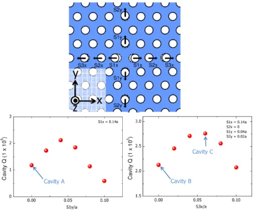
mode. There are several types of nanocavities proposed in the liter-ature. The main ones [5] are micropillars, microdisks and photonic crystals. Of these, photonic crystal cavities, which are point defects in a regular photonic crystal, are promising systems to achieve this purpose. These cavities can have high quality factors and low modal volumes even in the optical regimen, with the benefit that they can be embedded in a solid state system, enabling the insertion of emitters as quantum dots. There are many works focused in the optimiza-tion of the fracoptimiza-tion Q/V in photonic crystal cavities through small perturbations of their geometrical parameters.Figure1shows the re-sults obtained for theQoptimization in a photonic crystal slab cavity maintaining the modal volume not bigger than6% of its initial value. The largest values of the quality factor in these calculations have an order of magnitude of 105. These results were taken from reference [6].
The enhancement of the spontaneous emission of a light source within a cavity is determined by the Purcell factor, which is proportional to the fractionQ/V. Therefore, the quality factorQand the modal volumeV become very important parameters in the cavity quantum electrodynamics area.
Figure1: Scheme and results for the Q optimization of a photonic crystal slab cavity.S1x,S2x,S3x,S1yandS2ycorrespond to the hole shifts.
Cavity B and C have aQfactor about twice of the value for cavity A. Taken from reference [6].
1.2 nonlinear photonic crystals 5
Q factor is inversely proportional to the width of the transmission peak, the detection limit of such sensors is determined by the quality factor of the cavity. In this way, a higherQproduces a high precision sensor.Figure2shows the results obtained for theQoptimization in a nanobeam photonic crystal cavity; there are showed the system and the geometrical parameters (top), the behavior of Q as function of these parameters and the refractive index (bottom-left), the transmis-sion spectrum of the cavity sensing at different sample concentrations and the wavelength mode as function of the refractive index and
tem-perature. These results was taken from reference [7]. The shift induced in the resonance frequency of a photonic crystal cavity by a liquid, in which the crystal was immersed, can be used to determine the refraction index of the liquid. Therefore, the quality factor of the cavity determines a limit in the precision of this sensing.
Figure2: (Top) Scheme of a nanobeam photonic crystal cavity. (Bottom-left) Results for the behavior of Q and sensitivity as functions of the geometrical parameters and the refractive index of the crystal. (Bottom-right) Results for the transmission spectrum of the cavity at different sample concentrations, and its wavelength fundamen-tal mode refractive index and temperature dependences. Taken of the reference [7].
1.2 nonlinear photonic crystals
trans-6 state of the art
mission for the same input signal. To achieve bistability in photonic structures it is necessary to embed a nonlinear material, such as a Kerr-type one which induces a electric field intensity dependence in the refractive index.??shows the transmission spectrum of a waveg-uide bend with three embedded defects made of Kerr-type nonlinear material for two different input powers (left), and the transmission as a function of the input power showing bistability phenomena in the response function of the structure. These results was taken of the reference [8]. Reference [9] is another important work in this topic.
Nonlinear properties of photonic crystal circuits are required to achieve all-optical signal processing.
Figure3: (Left) Transmission spectrum of a waveguide bend with embed-ded Kerr-type nonlinear material for two different input powers (solid and dashed lines). (Right) Transmitted light as function of the input power showing bistability phenomena. In the diagram of the structure shown in the inset, the black circles represent the Kerr-type materials. Taken of the reference [8].
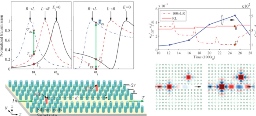
Since the first works in nonlinear photonic crystals, beginning with Berger [10], there is great interest to obtain efficient all-optical switches and all-optical transistors based in photonic crystals with embedded nonlinear materials. Nozaki et al. [11] proposed and built an optical switch which consumes sub-femtojoule energies to operate. The ba-sic principle of operation is based in the nonlinear properties of the cavity material used in the system.Figure4shows the scheme of the photonic switch; the pump power has the function to control the reso-nance frequency of the H0nanocavity and determine the states “off” and “on” of the switch: when there is an input pump power the re-fractive index of the cavity increases, then the resonance frequency decreases and the wavelength increases consequently. Therefore, as is showed in the bottom-left of the Figure (dashed lines), the transmis-sion goes to zero and the signal is not transmitted. When there is not an input pump power, the resonance frequency of the cavity coincides with the frequency of the input signal and therefore it is transmitted. In the bottom-right, the intensity distribution of the fundamental H0
mode, which has a very low modal volume, is shown. An interesting work in which an optical transistor based in the all-optical switching is studied, is discussed in the reference [12].
1.3 fano resonances and their applications 7
all-optical microprocessors chips.Figure5, taken of the reference [13], shows the schematization of an all-optical gate in a photonic crystal slab (top-right) based on the same idea of the all-optical switching shown in Figure 4. The two cavities shown inFigure 5 are made of nonlinear materials. The table of theFigure5shows the principles of
the gates AND, NAND, OR and NOR in this all-optical system. All-optical switching is the basic principle of operation of all-optical transistor and logic gates, which will be the fundamental components of an all-optical microprocessor.
Figure4: (Top) Structure of the photonic crystal switch; the input pump con-trols the states “off” and “on” of the switch, determining a zero or total transmission of the signal, respectively. (Bottom-left) Princi-ple of operation of the switch. (Bottom-right) Intensity distribution of the fundamental H0cavity mode. Taken of the reference [11].
For the gate AND, the fundamental resonances of the two cavities are
f1 andf2 respectively, with the conditionf1=f2. The initialization is
f1 6=f0, wheref0 is the frequency of the input signal. There are two normally incident pump lightsI1andI2associated to the logic states. When there is onlyI1 the power is not sufficient to shift the resonance of f1 to f0 (f16=f0), and the signal is not transmitted (logic0). When there is only I2 the results is also f2 6= f0 (logic 0), however, when there areI1andI2the power is sufficiently high to makef1 =f0, and the signal is totally transmitted (logic 1). The principles of the other gates NAND, OR and NOR share the same idea.
1.3 fano resonances and their applications
dis-8 state of the art
Figure5: (Top-left) Nonlinear response of the cavity resonance to the power of the pump light. (Top-right) Diagram of the all-optical gates based in a photonic crystal structure. (Bottom) Principles of all-optical gates AND, NAND, OR, and NOR. Taken of the reference [13].
1.4 quantum well infrared photodetectors 9
are the nonlinear cavities. The intensities of the RL and LR regimes as well as the contrast ratio are shown in the top-right, and the electric field distributions are shown in the bottom-right. Clearly the contrast
is high between the two operating states. The asymmetric sharp peak of Fano resonances produces a very high variation in the transmission function of the photonic structure in a range narrower than the full width of the resonance itself.
Figure6: (Top-left) Comparison between Lorentzian-shape and Fano-shape spectrums for the linear (solid line) and nonlinear regimes (dash-dotted and dashed lines): ω0 is the frequency of the linear reso-nance,ωi is the frequency of operation,TRL andTLRare the
trans-missions for the two operating states right to left and left to right respectively. (Bottom-left) Scheme of the photonic structure, C1
andC2are the nonlinear cavities. (Top-right)IRL,ILRandC(Ii)as
functions of time. (Bottom-right) Electric field distributions in the two operating states of the diode. Taken of the reference [15].
1.4 quantum well infrared photodetectors
quan-10 state of the art
tum well photodetector embedded in a photonic crystal slab. The first order mode have its electric field highly concentrated in the center of the structure (photodetector region). In bottom the results for the de-tectivity, detectivity enhancement and signal enhancement are shown with respect to the standard QWIP (illuminated at45◦). The photonic crystal slab quantum well infrared photodetector (PCS-QWIP) can be
20times more efficient than the standard QWIP.
Photonic crystal slabs can be used to enhance the absorption in quantum well infrared photodetector through a resonant coupling with the crystal modes.
Figure7: (Top) Photonic crystal slab quantum well infrared photodetector (PCS-QWIP), the first order mode is highly concentrated in the center of the slab, which is the QWIP region. (Bottom) Results for the detectivity, detectivity enhancement and signal enhancement with respect to the standard QWIP. Taken of the reference [18].
1.5 summary
2
F U N D A M E N TA L T H E O R YWhen a wave propagates in a dispersion medium, it undergoes multi-ple scattering if the wavelength involved is comparable with the size of the scatterers. In particular, the electrons or electron waves undergo multiple scattering in periodic arrays of atoms or atomic crystals. Con-structive interference between the electronic waves originates allowed electronic states as valence and conduction bands, on the other hand, destructive interference originates forbidden electronic states. The al-lowed electronic energies are represented by bands and the forbid-den ones by electronic band gaps. Analogously, the photons or elec-tromagnetic waves undergo multiple scattering in periodic arrays of dielectrics. A material in which there is a periodic variation of the di-electric function, with period that is of the same order of magnitude of the wavelength involved, is usually called a photonic crystal. In the same manner as for an atomic crystal, in a photonic crystal construc-tive interference originates bands or allowed states and destrucconstruc-tive interference originates photonic band gaps or forbidden states. In this way, the physical origin of the photonic band gaps and the electronic band gaps is, in essence, the same: interference phenomena produced by multiple scattering in a medium with a periodic distribution of scatterers. Whereas the electronic band gaps are produced in atomic crystals, the photonic band gaps are produced in photonic crystals. Therefore, it is expected that a large number of features that charac-terize atomic crystals are inherited by photonic crystals, such as Bra-vais lattices, primitive cells, Brillouin zones, energy bands, impurity bands and Bloch states. Nevertheless, there are important differences: the electron dynamics is governed by the scalar Schrödinger equation, whilst the electromagnetic dynamics is governed by the fully vectorial Maxwell equations. Another important difference is related with the statistical nature of the electrons; since electrons are fermions the in-teractions electron-electron are relevant in atomic crystals, in contrast to photon-photon interactions, which at typical energies in photonic crystals can be neglected.
Even though in photonic crystals literature the word photon is widely used, the emergence of band gaps can be explained through a classi-cal treatment of the Maxwell equations in materials with a periodic refractive index. It is important to mention that the principal char-acteristic of photonic crystals is their capability to modify the electro-magnetic density of states, which can affect dramatically the radiative
12 fundamental theory
dynamics of active systems immersed in such crystals.
In this chapter a quick review is made of the fundamentals of solid state physics and electromagnetism in inhomogeneous media, theo-retical pillars in the study of photonic crystals.
2.1 fundamentals of solid state physics
The characterization of the electronic states in atomic crystals is ad-dressed in the solid state physics. In this way, a mathematical and physical understanding of the concepts underlying their methods and interpretations is of great importance to embark the study of the physical mechanisms that characterize the photonic states in periodic media.
Bravais lattice
In the study of any crystalline solid it is very important the concept of Bravais lattice; this specifies a periodic array in which the basic units of the crystal are organized. Such basic units can be atoms, molecules, or in general, an atomic basis with an arbitrary number of particles. The Bravais lattice contains all the geometrical informa-tion about the crystalline structure, without any specificainforma-tion of its composition. Mathematically, a Bravais lattice is defined as all the points of the space whose vector positionRcan be written as a linear combination, with integer coefficients, of the primitive lattice vectors
a1,a2 anda3:
R=n1a1+n2a2+n3a3. (1) It is said that the vectorsa1,a2 anda3 generate or expand the crystal lattice, and the vectorRis called the lattice vector.
Primitive cell
That portion of volume, area or length, which fills the space under translations of the lattice vector, without overlapping of neighboring portions, is known as the primitive cell or primitive unit cell of the lattice. A primitive cell contains only one lattice point, therefore, if n
2.1 fundamentals of solid state physics 13
Reciprocal lattice and Brillouin zone
Given a arbitrary plane wave eik.r and a Bravais lattice described by a lattice vector R, it is possible to choose a set of G vectors which make the plane wave inherit the periodicity of the lattice. the set of
G′s determine a lattice known as the reciprocal lattice, which is the Bravais lattice in k or Fourier space. Mathematically, the reciprocal lattice is defined as:
eiG·(r+R)=eiG·r. (2)
Since the reciprocal lattice is another Bravais lattice, in the same way as in real space, the reciprocal primitive lattice vectorsb1,b2 andb3 are defined as the vectors which expand such lattice, and the recipro-cal lattice vector as a linear combination, with integer coefficients, of the primitive vectors:
G=m1b1+m2b2+m3b3. (3) The Wigner-Seitz cell of the reciprocal space is known as the first Brillouin zone. The vectors in the real and reciprocal space are related through the following expressions:
bi·aj=2πδij, G·R=2πl, (4) wherelis an integer number.
Bloch’s theorem
Bloch’s theorem states [19]:The eigenstatesψ of the one-electron Hamil-tonianH= − h22m∇2 +U(r), whereU(r+R) =U(r) for allRis a Bravais lattice, can be chosen to have the form of a plane wave times a function with
the periodicity of the Bravais lattice: In the theory of ordinary differential equations an equivalent form of the Bloch theorem is called the
Lyapunov-Floquet theorem.
Ψnk(r) =eik·runk(r). (5)
Where n is the band number, k is the wave vector and unk(r) is a
periodic function with the periodicity of the Bravais lattice: unk(r+ R) = unk(r). The eigenstate of expression (5) is called a Bloch state.
The Bloch states are subject to the boundary condition:
Ψnk(r+R) =eik·RΨnk(r). (6)
For all Rin a Bravais lattice. The condition (6) is known as the Bloch boundary condition.
Energy bands
14 fundamental theory
find the energy functionE(k), which is the dispersion relation or the energy bands of the electron in the atomic crystal. Since the reciprocal lattice is a Bravais lattice, the dispersion relation can be parametrized translating the function E(k) to the first Brillouin zone, subtracting from k the appropriated reciprocal vector. The equivalents vectors
k and k+G corresponds to the same point in this zone, however
E(k)6=E(k+G). Therefore, it is convenient to introduce a new index
n, known as the band index, to represent the values of E(k)
asso-ciated to each translation of k to the first Brillouin zone from the another ones. Being n the band index, En(k) is the correct form to represent the energy for one electron with a wave vectorkin the first Brillouin zone. This convention which indexes the electron energies is known as the reduced scheme zone.
2.2 fundamentals of electromagnetism
The electromagnetic states in a photonic crystal are governed by the wave equation in inhomogeneous media, which can be written as an eigenvalue problem whose differential operator is Hermitian. This fact is of great importance, since most of the quantum mechanical the-ory of observables can be directly applied in the characterization of the photonic crystal through a fully treatment. In this way, the theory of photonic crystals takes advantage of the methods used in quantum mechanics to describe the scattering dynamics of classical electromag-netic fields in periodic media. See for example the reference [20].
Since photonic crystals are dielectric systems, their physical properties are described by the electromagnetic theory.
Maxwell equations and wave equation
The electromagnetic field dynamics is described by the Maxwell equa-tions which in MKS units, when free charges and electric currents are absent, take the form:
∇ ·D(r,t) =0,
∇ ·B(r,t) =0,
∇ ×E(r,t) = − ∂
∂tB(r,t), ∇ ×H(r,t) = ∂
∂tD(r,t). (7)
WhereE,H,DandBare the electric, magnetic, electric displacement and magnetic induction fields respectively. The fields Hand B, and
E and Dare related by the known constitutive relations [21]. In the usual treatment of photonic crystals nonmagnetic materials are con-sidered, therefore, the magnetic permeability of the medium is the same as for the free space, and the constitutive relation between H
andBis written as:
2.2 fundamentals of electromagnetism 15
The dielectric function of the medium will be assumed real, isotropic and frequency independent. In this way, ifǫ0is the dielectric constant of vacuum and ǫ(r) is the relative dielectric function of the medium, the constitutive relation betweenEandDis written as:
D(r,t) =ǫ0ǫ(r)E(r,t). (9) Replacing the relations (8) and (9) in the equations (7), the Maxwell equations take the form:
∇ ·ǫ(r)E(r,t) =0,
∇ ·H(r,t) =0,
∇ ×E(r,t) = −µ0
∂
∂tH(r,t), ∇ ×H(r,t) =ǫ0ǫ(r)
∂
∂tE(r,t). (10)
In order to obtain the relations that govern the propagation of the fields HandE independently, equations (10) are decoupled through simple vector identities leading to the electromagnetic wave equa-tions:
∇ × 1
ǫ(r)∇ ×H(r,t) = −
1 c2
∂2
∂t2H(r,t), (11)
1
ǫ(r)∇ × ∇ ×E(r,t) = −
1 c2
∂2
∂t2E(r,t), (12) wherec, the speed of the light in vacuum, is defined as √µ1
0ǫ0. In
gen-eral, HandE are complicated functions of space and time. Since the Maxwell equations are linear, it is possible to separate the time and space dependence expanding the fields in a set of harmonic modes. For one harmonic mode the fields become:
H(r,t) =H(r)e−iωt,
E(r,t) =E(r)e−iωt. (13) This is not a great limitation because it is known by Fourier analysis that any time dependence in the fields can be described as a suitable combination of this kind of modes. With the expressions (13), the wave equations reduce to:
ˆ
ΘH(r) =∇ × 1
ǫ(r)∇ ×H(r) =
ω2
c2 H(r), (14) ˆ
LEE(r) = 1
ǫ(r)∇ × ∇ ×E(r) =
ω2
16 fundamental theory
Eigenvalue problems
The equations (14) and (15) establish ordinary eigenvalues problems with differential operators ˆΘand ˆLErespectively. These problems are implicitly dependent on each other, since the fields H and E are re-lated through the Maxwell equations. Hence, the solution of any one automatically determines the solution of the other. It is important to mention that the operators ˆΘand ˆLEare linear, so that any linear com-bination of the solutions is also a solution. The key difference between equations (14) and (15) is that ˆΘ is an Hermitian operators, whilst
ˆ
LE is not. Therefore, the eigenvalue problem (14) is essentially sim-pler than the problem (15). The Hermiticity of ˆΘ evokes the known spectral theorem of quantum mechanics, which states that the eigen-values of an Hermitian operator are real and the eigenfunctions of such operator form a basis for the space of states and, for different eigenvalues, are orthogonal [22]. In this way, the following relations are guaranteed:
The analogy between quantum mechanical formalism and the electromagnetic treatment of inhomogeneous media, allows taking advantage of the theoretical methods used in atomic crystals to apply them in photonic crystals.
ω2
c2 =
ω2 c2 ∗ , Z
H∗i(r)·Hj(r)d3r=N2δij. (16) WhereNis a normalization factor. In addition, it is possible to show that for ǫ(r) > 0, ˆΘ is positive semidefinite, i.e., ωc22 > 0. Under this
condition, the frequenciesωare always real numbers [23].
Variational principle
In analogy to quantum mechanics, the electromagnetic variational principle establishes a connexion between the concentrations and os-cillations of the fields (wave functions) in the medium (potential), and the energies associated to these normalized distributions, keeping the orthogonality between the eigenstates of the Maxwell operator. For-mally, the variational principle assigns the minimum eigenvalue ω20
c2,
and consequently the mode of lower frequency, to the field H0 that minimizes the functional:
Φ[H] =
R
H∗(r)·ΘHˆ (r)d3r
R
H∗(r)·H(r)d3r . (17) The functionalΦis known as the Rayleigh-Ritz quotient. The next low frequency mode will minimize Φ within the subspace of functions orthogonal toH0. The variational expression (17), written in terms of the electric field, takes the form:
Φ[E] =
R
|∇ ×E(r)|2d3r R
2.2 fundamentals of electromagnetism 17
Expression (18) establishes that the way to minimize the functionalΦ
is concentrating the electric field in regions of high dielectric dielectric constant and minimizing the spatial oscillations [23].
Electromagnetism in periodic media
When ǫ(r+R) = ǫ(r), for any R in a Bravais lattice, the dielectric function represents a photonic crystal or medium with periodic re-fractive index. The concepts of primitive cell and Wigner-Seitz cell remains unaltered in these arrays whose atomic basis is composed of dielectric materials. The electromagnetic field description is realized through the Bloch theorem, therefore,EandHare represented as the product of a plane wave and a periodic function with the periodicity of the lattice. In the same way, the dispersion relation or photonic band diagramωn(k)is constructed in the first Brillouin zone, which can be reduced taking advantage of the symmetry properties of the crystal 1. A formal treatment about group theory and symmetries in photonic crystals is realized in the reference [24].
Part II
3
P L A N E WAV E E X PA N S I O N M E T H O DThe plane wave expansion method (PWE), or Fourier expansion, ploits the periodicity of the dielectric system to make a periodic ex-pansion of the fields and the dielectric function in a plane wave basis. Such expansion is introduced in equations (14) and (15) to obtain a system of infinite algebraic equations through simple integral orthog-onality relations. In principle, any functional basis can be used to expand the fields in photonic crystals [25], however, the plane wave basis is quite simple in their mathematical structure, and makes a very good description of the crystals studied in the present work.
In this chapter a general review is made of the PWE method applied to two-dimensional photonic patterns with infinite thickness. The principal purpose is to give a background for the scattering matrix treatment which is studied inChapter4. Studies of photonic crystals with the PWE method can be reviewed in the references [26,27,28].
3.1 two-dimensional photonic crystal
A two-dimensional photonic crystal consists of a two-dimensional pe-riodic pattern in a plane (xyplane for example), and a non-periodic or homogeneous pattern in the other dimension. Particularly, here will be studied crystals with general periodic patterns in thexyplane, and a homogeneous distribution in z direction (infinite thickness). Since there is a reflection symmetry plane at any value ofz, due to the in-finiteness and homogeneity in this direction, the wave vector of the crystal resonances must be totally contained in the planexy. This fact classifies all the resonances in two distinct polarizations sets or sym-metries: transverse electric (TE) and transverse magnetic (TM). The former, in which the electric field is confined to thexyplane, has the non-zero fields components Hz, Ex and Ey. The latter, in which the magnetic field is confined to the xy plane, has the non-zero fields componentsEz,Hx andHy.
TE case
TE modes have electric and magnetic information, consequently any of the equations (14) or (15) can be used to find the solutions. How-ever, the magnetic field wave equation (14) is easier to solve since only one of the magnetic components is different from zero, so that the di-mensionality of the magnetic problem is smaller than the electric one.
22 plane wave expansion method
Once the component Hz is found, it is possible to find Ex and Ey through Maxwell equations (10). As it was mentioned inSection2.2, in periodic mediaHzcan be written as a Bloch state (5):
The fundamental principle of the PWE method is to make an expansion of the all periodical functions in the crystal using a plane wave basis.
H(r) =zHˆ z(x,y) =zHˆ zP(x,y)eik||·r, (19) where k|| = xkˆ x+ykˆ y and HPz(x,y) is a periodic function with the periodicity of the lattice. There is no dependence in z because the system is homogeneous in this direction. The key of the PWE method is to expand HPz(x,y) and ǫ(x1,y) in a plane wave basis whose wave
vectors determine the reciprocal lattice (2):
HPz(x,y) =
X
G
CGeiG·r, (20)
1
ǫ(x,y) =η(x,y) =
X
G
ηGeiG·r, (21)
where G = xGˆ x+yGˆ y is the reciprocal lattice vector (3), and the summation indexGindicates a symmetric sum over the all reciprocal vectorsG. From expressions (20) and (19), the total magnetic field in
ztakes the form:
H(r) =zˆX
G
CGei(G+k||)·r. (22)
The expressions (21) and (22) are replaced in equation (14):
∇ ×X
G′
ηG′eiG ′
·r∇ ×zˆX
G
CGei(G+k||)·r
=ω
c 2
ˆ
zX
G
CGei(G+k||)·r. (23)
Considering the following vectorial identities:
∇ ×zfˆ (x,y) = (x∂ˆ y−y∂ˆ x)f(x,y),
∇ ×xfˆ (x,y) = −z∂ˆ yf(x,y),
∇ ×yfˆ (x,y) =z∂ˆ xf(x,y), (24) the vectorial equation (23) is reduced to the following scalar equation:
X
G′G
ηG′CG
h
(Gx+kx)(G ′
x+Gx+kx) + (Gy+ky)×
(Gy′ +Gy+ky)
i
ei(G′+G)·r=ω
c 2X
G
CGeiG·r. (25)
3.1 two-dimensional photonic crystal 23
region of the plane wave basis RO, which is not necessarily the unit cell1. The integrals have the solutions:
Z
RO
ei(G′+G−G′′)·rda=AROδG′+G,G′′,
Z
RO
ei(G−G′′)·rda=AROδG,G′′. (26) The Kronecker delta functions produced in the integrals (26) simplify the equation (25), leading it to the final expression:
X
G
ηG′−G
h
(Gy′ +ky)(Gy+ky) + (G ′
x+kx)(Gx+kx)
i CG
=ω
c 2
CG′, (27)
where the result Gi′′ = Gi′ +Gi obtained in (26) was used, and the dummy indexG′′ was replaced byG′.
TM case
Taking into account that the only non-zero components of the TM modes areEz,HxandHy, and under the same argument exposed for the TE modes, the solution is obtained for theEzcomponent through the equation (15). In this way, the electric field can be written as a
Bloch state: Even though theE
eigenvalue equation has only one component in the TM case, the eigenvalue problem is not Hermitian, therefore, a slow convergence is expected. E(r) =zˆX
G
CGei(G+k||)·r. (28)
The function ǫ(x1,y) is expanded in the same way as for the previous TE case, and the expressions (21) and (28) are replaced in equation (15):
X
G′
ηG′eiG ′
·r∇ × ∇ ×zˆX
G
CGei(G+k||)·r
=ω
c 2
ˆ
zX
G
CGei(G+k||)·r, (29)
which is reduced, using the vectorial identities (24), to the following scalar equation:
X
G′G
ηG′CG(Gx+kx)2+ (Gy+ky)2
ei(G′+G)·r
=ω
c 2X
G
CGeiG·r. (30)
24 plane wave expansion method
At this point, equation (30) is multiplied by e−iG′′·r, and integrated
using the results (26), to obtain the final eigenvalue problem:
X
G
ηG′−G(Gx+kx)2+ (Gy+ky)2
CG=
ω c
2
CG′, (31)
where the dummy indexG′′ was changed toG′.
Note that expressions (27) and (31) are eigenvalue systems of alge-braic equations whose eigenvalues are ωc2, and whose eigenvectors are determined by the CG coefficients. The plane wave basis must be truncated in these expressions to solve numerically the problem.
3.2 supercell approach
When an impurity or defect is introduced into the crystal, localized modes can arise in the structure, with energies in the photonic band gap. The rigorous description of defects is made through calculations in finite crystals [29], nevertheless, the complexity involving this kind of studies suggests the introduction of approximations that simplify the problem, maintaining an accurate representation of the system.
When the periodicity of the crystal is broken with defects, it is possible to restore it considering such defects inside a periodic larger cell or supercell.
The supercell approach is one of these approximations. It consists in restoring the periodicity of the crystal considering a bigger “prim-itive cell”, called supercell, with the defect inside it. The complete crystal is built replicating the supercell under translations of the lat-tice vector in the new Bravais latlat-tice, without overlapping between neighboring supercells. In this manner, the description of the fields in the defective crystals can be made through Bloch states and any method based in this kind of states and the periodicity of the system will be also valid for crystals with defective supercells. If there is a suf-ficiently large distance between consecutive defects allowing one to neglect the overlapping of their electromagnetic fields, the supercell approach is said to be good. It is important to say that if the magni-tude of lattice vector in the supercell is larger, the magnimagni-tude of the reciprocal lattice vector becomes shorter in relation to those without supercell considerations (regular lattice). This fact implies a reduction of the Brillouin zone size, and thekvectors will suffer a higher num-ber of translations in a reduced zone scheme. In this way, the bands associated to the supercell are folded with respect to ones associated to the regular primitive cell, due to the additional translations of k
needed to describe the complete system in a smaller Brillouin zone. To clarify this, suppose a one- dimensional crystal with lattice vector
3.3 implementation 25
will be affected by a factor of one-half, B = 12b. The new Brillouin zone has a size of πa; so that, the vectors k lying between πa and 2πa becomes linearly dependent to those lying between 0 and πa. There-fore, in a reduced zone scheme the bands associated tok between πa and 2πa are translated to the new first Brillouin zone defined between
0 and πa, producing an apparent folding of the bands with respect to the crystal with regular primitive cell. For more details consult refer-ence [30].
3.3 implementation
4
S C AT T E R I N G M AT R I X M E T H O DThe scattering matrix method (SMM) is a powerful tool to solve the problem of the scattering by a large finite number of objects. Basi-cally, the method studies the individual scattering by each object and then evaluates the coupling phenomena between them. Even though the treatment of the electromagnetic fields in the SMM is quite rigor-ous, it is based on an intuitive physical idea: the fields scattered by the structure are causally related with the fields incident in it. In the photonic crystal area, the SMM has been used to solve the scattering properties of finite two-dimensional periodic arrays of cylinders, el-lipses and squares [29, 32, 33]. Nevertheless, such scattering objects have an infinite length in the non-periodic direction, which is a great limitation to study photonic crystals with finite thickness, known as photonic crystal slabs. To overcome this difficulty Whittaker and Cul-shaw [34] proposed a new approach: they solve the problem trans-ferring the infiniteness in the perpendicular direction of the periodic pattern to the extent of the pattern itself. In this way, the photonic structure consists of a multilayer system with periodic infinite pat-terns perpendicular to the layer growth direction. Each layer has a finite thickness and represents a complex scattering object which cou-ples to the other ones. Initially, the scattering matrix treatment of this kind of systems was applied by Ko and Inkson [35] to solve the electron tunneling in multilayer semiconductor heterostructures; the work [34] is nothing more than the electromagnetic equivalent formu-lation for photonic structures.
The scattering matrix treatment applied to multilayer photonic struc-tures can be summarized as follows: the band structure is solved in each layer to describe the states in the direction perpendicular to the pattern as simple plane waves; these states are used to represent the electromagnetic field in terms of forward and backward propagating waves; the scattering matrix is calculated using this representation, and finally, the problem is completely solved applying the boundary conditions of the electric and magnetic fields in each interface of the multilayer system. Once the scattering matrix is obtained, it is possi-ble to relate the outgoing waves to the incoming ones in the structure, which allow the calculation of diffractive properties as the reflection and transmission.
In this chapter the main aspects of the method, which is developed in detail in the original work of Whittaker, are presented. Some new
28 scattering matrix method
contributions are made in the description of the incident field and the calculation of the reflectivity.
4.1 maxwell equations in the momentum representation
If a time harmonic dependence is considered for the fields (as it was discussed in Section 2.2), the electric field is rescaled as ωǫ0E → E and the frequency is rescaled as √µ0ǫ0ω = ω/c → ω, the Maxwell curl equations (10) take the following form:
∇ ×H(r||,z) = −iǫ(r||,z)E(r||,z),
∇ ×E(r||,z) =iω2H(r||,z), (32)
where thezdependence has been made completely explicit. The equa-tion∇ ·E=0is automatically satisfied in the curl equation ofH, and
∇ ·H = 0 is satisfied if the expansion ofH is made in a zero diver-gence basis. Since the layers of the system are composed by photonic structures, the magnetic and electric fields in each layer can be written as Bloch states:
H(r||,z) =X
G e
Hk||(G,z)e
i(k||+G)·r||,
E(r||,z) =X
G e
Ek||(G,z)e
i(k||+G)·r||. (33)
Note that the periodic pattern is contained in the xy plane, and the growth direction of the structure isz. The expressions (33) are more general than the (22) and (28) ones, since the expansion coefficients, and consequently the fields, have a functional dependence in z. The explicit reciprocal lattice vectorGis also considered in the functional dependence of the expansion coefficients and in the summation index, which is different fromSection 3.1 where only the magnitude of G
was written to specify the indexes; this is made with the purpose to use a more appropriate notation in the mathematical developments discussed below.
The fields can be represented as column vectors whose components correspond to their Fourier coefficients in the expansions (33), and the dielectric function as a square matrix populated by its expansion coefficients in a plane wave basis:
h(z) =hHek||(G1,z),Hek||(G2,z),· · ·
iT ,
e(z) =hEek||(G1,z),Eek||(G2,z),· · ·
iT ,
ˆ
ǫG′G(z) =eǫ(G ′
−G,z) = 1
ARO
Z
RO
ǫ(r||,z)e−i(G′−G)·r||. (34) In this wayh,eand ˆǫare the momentum representation ofH,Eand
4.2 band structure and expansion of the in-plane fields 29
AROrepresents the area where the plane wave basis is orthogonal as was discussed inSection3.1. The Maxwell curl equations (32), written in this representation, take the form:
ikˆyhz(z) −h ′
y(z) = −iǫeˆ x(z),
hx′(z) −ikˆxhz(z) = −iǫeˆ y(z),
ikˆxhy(z) −ikˆyhx(z) = −iǫeˆ z(z),
ikˆyez(z) −e ′
y(z) =iω2hx(z),
ex′(z) −ikˆxez(z) =iω2hy(z),
ikˆxey(z) −ikˆyex(z) =iω2hz(z), (35) where ˆkx and ˆky are diagonal matrices with components (kˆx)GG = kx+Gx and (kˆy)GG = ky+Gy respectively, and the primes denote differentiation with respect toz.
4.2 band structure and expansion of the in-plane fields
The purpose here is to solve the band structure in the periodic pattern of each layer to obtain states whose zdependence are in the form of plane waves. A convenient symmetric expansion of the magnetic field, which has zero divergence, is:
H(r||,z) =X
G
φx(G)
ˆ
x− 1
q(kx+Gx)zˆ
+
φy(G)
ˆ
y− 1
q(ky+Gy)zˆ
ei(k||+G)·r||+iqz. (36)
The band structure of the
two-dimensional periodic pattern is used to obtain states that propagate in the direction
perpendicular to the pattern.
Hereφx(G)andφy(G)are the expansion coefficients, andqdenotes wave number inz direction. In the momentum representation φx =
[φx(G1), φx(G2),· · ·]T and φy = [φy(G1),φy(G2),· · ·]T, therefore, the magnetic field of the expression (36) is represented as:
h(z) =eiqz
φxxˆ+φyyˆ−
1
q(kˆxφx+kˆyφy)zˆ
. (37)
Replacing (37) in the equations (35) and multiplying by iηˆ, where ˆ
ηǫˆ = 1, the momentum representation for the electric field is ob-tained:
e(z) = 1
qe
iqz ˆ
ηˆ
kykˆxφx+ (q2+kˆykˆy)φy
ˆ
x−
ˆ
kxkˆyφy+ (q2+kˆxkˆx)φx
ˆ
y+qkˆyφx−kˆxφy
ˆ
30 scattering matrix method
With the field representationsh(z)ande(z), equations (35) determine two linear independent identities:
ω2φx=
ˆ
kyηˆkˆy+η qˆ 2+kˆxkˆx
φx+
ˆ
ηkˆxkˆy−kˆyηˆkˆx
φy,
ω2φy=
ˆ
kxηˆkˆx+η qˆ 2+kˆykˆy
φy+
ˆ
ηkˆykˆx−kˆxηˆkˆy
φx.
(39) The two identities (39) are reduced to the following eigenvalue prob-lem forω:
H(q2+K) +Kφ=ω2φ, (40)
where the blocks2×2 K,H,Kand the vectorφare defined as:
K= kˆxkˆx kˆxkˆy
ˆ
kykˆx kˆykˆy
!
, H= η 0ˆ
0 ηˆ
!
,
K= kˆyηˆkˆy −kˆyηˆkˆx −kˆxηˆkˆy kˆxηˆkˆx
!
, φ= φx
φy
!
. (41)
The band structure of the two-dimensional photonic crystal with infi-nite thickness (Section3.1) can be calculated using equation (40) mak-ing q = 0. Reorganizing the terms in equation (40), the eigenvalue problem forqis written as:
E ω2−K−Kφ=q2φ, (42)
whereEis a diagonal block matrix2×2of ˆǫ, and satisfiesEH=1. It is important to mention that the quantities q, in the eigenvalue prob-lem (42), can be complex even ifEis real.
The in-plane components of the fields, in each layer of the structure, can be expanded in terms of forward and backward propagating waves with wave umbersqn, and amplitudesanandbnrespectively, which are determined through the continuity conditions in each in-terface of the structure. In the momentum representation such expan-sion takes the form:
hx(z)
hy(z)
!
=X
n
φxn φyn
!
eiqnza
n+eiqn(d−z)bn
, (43)
The forward and backward plane waves are natural solutions of the wave equation when the medium is homogeneous, which is the case of each layer in thez direction.
wheredis the thickness of the layer. An arbitrary sign inqnis chosen to makeIm{qn}> 0and prevent exponential growths in thez depen-dence, which would make the method unstable. The expansion (43) can be written is a more compact form:
h||(z) =Φ ˆ
f(z)a+fˆ(d−z)b, (44) where Φ is a matrix with columns φn, ˆf(z) is a diagonal matrix with components ˆf(z)nn = eiqnz. h||(z), a and b are column
4.3 scattering matrix 31
(b1,b2,· · ·)T respectively. In a similar way, using the expressions (37) and (38), the eigenvalue equation (40) and the magnetic field expan-sion (43), the equivalent electric field expansion is obtained:
−ey(z)
ex(z)
!
=e||(z) = ω2−KΦqˆ−1fˆ(z)a−fˆ(d−z)b, (45)
where ˆqis a diagonal matrix with components ˆqnn=qn. The expres-sions for magnetic (44) and electric (45) fields can be compacted in a single matrix expression:
e||(z)
h||(z) !
=M fˆ(z)a
ˆ
f(d−z)b !
, (46)
whereMis defined as:
M= ω
2−KΦqˆ−1 − ω2−KΦqˆ−1
Φ Φ
!
. (47)
4.3 scattering matrix
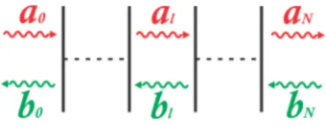
The scattering matrix relates the amplitudes of the forward and back-ward propagating waves in different layers of the structure:
al
bl′
!
=S(l′,l) al′
bl
!
= S11 S12
S21 S22
! al′
bl
!
. (48)
The subscriptldenotes the l-th layer in the multilayer media shown in Figure 8, where the forward and backward waves amplitudes are shown schematically. The fact that the scattering matrix relates the waves in different layers of the structure makes it numerically stable. It is not the case for the transfer matrix [36], in which the waves are related in the same layer, leading to numerical overflows for large
k+G [34]. The boundary conditions of e and h imply that e|| and
h|| must be continuous in each interface of the system, i.e., in z= d
for the layerl andz= 0for the layerl+1. Using the expression (46) these continuity relations become:
Ml ˆ
flal
bl
!
=Ml+1 al+1 ˆ
fl+1bl+1
!
. (49)
Here ˆfl =fˆl(dl). The relation (49) in terms of the matrixI(l,l+1) =
M−l1Ml+1, called interface matrix, takes the form:
ˆ
flal
bl
!
=I(l,l+1) al+1
ˆ
fl+1bl+1
!
= I11 I12
I21 I22
! al+1 ˆ
fl+1bl+1
!
32 scattering matrix method
The scattering matrix S(l′,l+1) can be calculated recursively from
S(l′,l)andI(l,l+1)defined in (48) and (50). Eliminating theaandb
dependences the block components ofS(l′,l+1)are:
S11(l ′
,l+1) = (I11−fˆlS12(l ′
,l)I21)−1fˆlS11(l ′
,l),
S12(l ′
,l+1) = (I11−fˆlS12(l ′
,l)I21)−1(fˆlS12(l ′
,l)I22−I12)fˆl+1, S21(l
′
,l+1) =S22(l ′
,l)I21S11(l ′
,l+1) +S21(l ′
,l),
S22(l ′
,l+1) =S22(l ′
,l)I21S12(l ′
,l+1) +S22(l ′
,l)I22fˆl+1, (51)
Figure8: Multilayer system. ai corresponds to the forward waves and bi
corresponds to the backward waves. Adapted from [34].
with the initial conditionS(l,l) =1. Since the matrix ˆf, which contains the evanescent behavior, is never inverted directly, the scattering ma-trix is stable throughout the structure. Denoting as l= 0the surface of the system and l = N its substrate, see Figure 8, the amplitudes
aandbin each layer are defined in terms of the matricesS(0,l) and
S(l,N):
The scattering matrix determines the causality relation between the waves entering in the system,a0and
bN, and the waves
scattered by it,b0
andaN.
al= (1−S12(0,l)S21(l,N))−1(S11(0,l)a0+S12(0,l)×
S22(l,N)bN),
bl= (1−S21(l,N)S12(0,l))−1(S21(l,N)S11(0,l)a0+
S22(l,N)bN). (52)
4.4 reflectivity and transmission
The calculation of the reflectivity and transmission in the structure requires the vector coefficients b0 and aN, which represent the re-flected and transmitted waves, respectively. With the scattering matrix
S(0,N) and the vector coefficienta0 (the incident field), it is straight-forward to obtainb0 andaN:
4.4 reflectivity and transmission 33
space field representation to calculate the diffractive properties. Equa-tion (46) accomplishes this translation:
e||(0)0
h||(0)0
!
Ref
=M0 0
ˆ
fl(d0)b0
!
,
e||(zt)N
h||(zt)N
!
T ra
=MN ˆ
fl(zt)aN
0 !
, (54)
where d0 and zt are the perpendicular distances from the structure at which the reflectivity and transmission are calculated respectively, and the vector bN is considered null since there is no field incident from the outside at the substrate. Taking into account that e|| =
[−ey,ex]T, h|| = [hx,hy]T and the z field components are obtained from thexandycomponents through Maxwell curl equations (35), it is possible to construct the field expansion from the expressions (33) atd0 for reflected fields and atzt for transmitted fields:
HRef(r||) = X
G
hRefx (0)Gxˆ+hRefy (0)Gyˆ +hRefz (0)Gzˆ
ei(k||+G)·r||,
ERef(r||) = X
G
eRefx (0)Gxˆ+eRefy (0)Gyˆ+eRefz (0)Gzˆ
ei(k||+G)·r||,
HT ra(r||) =X
G
hT rax (zt)Gxˆ+hT ray (zt)Gyˆ +hT raz (zt)Gzˆ
ei(k||+G)·r||,
ET ra(r||) =X
G
eT rax (zt)Gxˆ+eT ray (zt)Gyˆ+eT raz (zt)Gzˆ
ei(k||+G)·r||. (55) Here the superscripts Ref and T ra denote the reflected and trans-mitted fields, respectively. To obtain the vector a0 from the incident fields HandEtheir expansion coefficients, in the basiseiG·r||, are in-troduced into the corresponding components of h|| and e||, and the translating equation (46) is used again, but now inverted:
a0 =M−0,111e||+M−0,112h||. (56) Once the fields are expressed in the complex space, it is possible to calculate the reflectivity and transmission:
R= Φ Ref z ΦInc z
, T =
Φ T ra z ΦInc z
. (57)
Φz is the flux of the Poynting vector in zdirection across a desired areaA:
Φz=
Z
A
Sz(r||)da=
1 2ǫ0ωc
Z
A
34 scattering matrix method
When the integration is made in an area of orthogonality (ARO) of the plane waves eiG·r||, the integral (58) reduces to:
The general reflectivity and transmission coefficients are calculated through the flux of the Poynting vector across a desired area.
Φz=
ARO
2ǫ0ωc
Rehe†||·h||i. (59)
The operation† denotes the transposed-conjugated. Moreover, if the area of integration is a circle of radius r the integral (58) has the analytical solution1:
Φz =
πr ǫ0ωc
X
G′G J1
r|G′−G| |G′−G|
h e
e∗x(G)ehy(G ′
) −ee∗y(G)ehx(G ′
)i, (60)
where J1 is the Bessel function of order one. The equations (57) are generalized expressions to calculateRandT; when there is no pattern in the plane xythese quantities reduce to the square modulus of the well known Fresnel coefficients.
4.5 incident field
With the aim of making a general description of a linearly polarized incident field,HandEcan be initially written in the following form:
E=E0(cosαεˆ1+sinαεˆ2)ek||·r||,
H=H0(−sinαεˆ1+cosαεˆ2)ek||·r||,
k|| =k0sinθ(cosϕxˆ+sinϕyˆ), (61) where α(polarization angle), θ (incident angle) andϕ (polar angle) are defined in Figure 9, E0 = ǫ0ωcZ
1
2, H0 = Z− 1
2 and k0 = √ǫω
c.
Z = q µ0
ǫ0ǫ is the intrinsic impedance of the external medium with
dielectric constantǫ. The polarization vectors are defined as:
ˆ
ε1 =sinϕxˆ−cosϕyˆ, ˆ
ε2 =cosθcosϕxˆ+cosθsinϕyˆ−sinθzˆ. (62)
The TE and TM polarizations (Section3.1) correspond to the particu-lar casesαT E=0andαT M= π2 respectively.
In many situations it is necessary to provide a specific spot shape to the incident field; this is accomplished taking advantage of the plane wave basis that describes the system: since there is a complete basis, it is possible, in principle, to expand any shape of the incident field. In practical terms the dimension of the basis must have a cutoff because only problems with finite matrices can be solved numerically in a computer; however, if the dimension is large enough, the expansion will describe this arbitrary-shape field with good accuracy. With this in mind, an arbitrary-shape functionP(r||), defined to have maximum
4.5 incident field 35
Figure9: Scheme of the incident field in the structure.αis the polarization angle,θ is the incident angle,ϕ is the polar angle and the ˆεi are
the polarization vectors.
value1and minimum value0, can be expanded with the same plane wave basis used in the patterned multilayer system:
P(r||) = X
G e
P(G)eiG·r||. (63)
It is possible to take advantage of the plane wave basis to describe an arbitrary shape of the incident field.
The procedure for providing the geometrical shape of this function to the incident field is to multiply each component of such field by
P(r||), consequently, the incident vector coefficients in the momentum representation become: e|| h|| ! Inc =
−ey
ex hx hy =
−Ey
h e
P(G1),eP(G2),· · ·
iT
Ex
h e
P(G1),eP(G2),· · ·
iT
Hx
h e
P(G1),Pe(G2),· · ·
iT
Hy
h e
P(G1),eP(G2),· · ·
iT
. (64)
HereEx,Ey, Hx andHyare the field components in the expressions (61). In this way, the problem to provide a geometrical shape to the in-cident field is reduced to the calculation of the coefficientseP(G). With
Part III
5
I M P L E M E N TAT I O N O F T H E S C AT T E R I N G M AT R I XM E T H O D
The scattering matrix method, as it was studied inChapter4, is a very powerful tool to calculate the diffractive properties of patterned mul-tilayer structures. One special kind of these structures are photonic crystal slabs (PCS), which are two-dimensional photonic crystals with a finite thickness in the third dimension. In PCS there are two con-finement mechanisms for light [37]: the distributed Bragg reflection produced by the periodic refractive index pattern, which consists in constructive and destructive electromagnetic interference phenomena throughout the crystal, and the index guiding produced by the high contrast refractive index between the slab and the external medium, which can be understood as the total internal reflection when an aver-age refractive index for the slab is considered. PCS have become very interesting systems in the last years because their potential applica-tions, see Chapter 1, and easier fabrication techniques at submicron length-scales. For these reasons, it is important to make a detailed study of their diffractive physical properties, which can be accom-plished through the implementation of the scattering matrix method.
In this chapter it is presented how to implement the scattering matrix method in symmetric1 PCS with L3 cavities, which are very special defects introduced in photonic crystals2. The particularization to L3 cavities is made with the purpose to focus in their reflectivity calcula-tions, the principal results of this work (seeChapter6). Nevertheless, the development exposed here is general and can be applied to an-other kind of defects or non-defective PCS.
5.1 implementation
The scattering matrix method is implemented to calculate the reflec-tivity spectra of a L3 PCS cavity at normal incidence. Since there is no substrate in the photonic crystal, it can be considered as a three layer structure: a layer of thickness d interposed between two semi-infinite layers. In this way, the index l, defined in Section 4.3, takes the possible values0,1and2.Figure10ashows a scheme of the pho-tonic crystal in zdirection. The layer l = 1 has a dielectric function
1 Symmetric photonic crystal slabs are characterized by having no substrate, therefore, the material below the slab is the same material above it, and consequently there is a reflection symmetry plane in the middle of the slab.
2 SeeAppendix B.
40 implementation of the scattering matrix method
ǫ(x,y)which is constant alongzin the layer, and contains an hexag-onal photonic pattern of air holes in the plane3; the layersl= 0 and
l=2have a dielectric constant associated to air,ǫ=1; and the quan-tities a0,b0 anda2 represent the incident, reflected and transmitted waves respectively. A representative scheme of the reflectivity calcu-lation in the L3cavity is shown inFigure10b.EIncandHInc refer to the incident electric and magnetic fields respectively with wave vec-tor kInc, ϕ is the polarization angle, which is the same αat normal incidence as was defined in Figure 9. The red circle with radius rs (bigger one) in the figure corresponds to the incident excitation spot, and the green circle with radius ra (smaller one) corresponds to the integration area of the reflected Poynting vector. Both, excitation and reflected flux calculation, are made at the same distanced0away from the crystal, which is incorporated in the method as the thickness of a virtual interface separating the same medium, see equation (54).
The PCS can be seen as a system of one layer with finite thickness interposed between two semi-infinite layers.
Figure10: (a). Photonic crystal slab in thezdirection: the layerl=0,l =1
(with thicknessd) andl=2correspond to air, the photonic struc-ture and air respectively; the incident field is represented bya0,
the reflected one byb0, and the transmitted one bya2. (b)
Rep-resentative scheme of the reflectivity calculation: the subscripts
Incdenote the incident quantities,ϕis the polarization angle;rs
andra denote the radius of the incident spot and the radius of
the Poyting flux area respectively;d0is the distance at which the crystal is excited and at which the reflectivity is calculated.
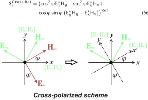
5.2 cross-polarized reflectivity calculations
Currently, it has become usual to measure reflectivity spectra of pho-tonic crystals by cross-polarized spectroscopy [38], which consists in