UNIVERSIDADE FEDERAL DO PARÁ INSTITUTO DE TECNOLOGIA
PROGRAMA DE PÓS-GRADUAÇÃO EM ENGENHARIA ELÉTRICA
GIANNI MASAKI TANAKA PORTELA
DISPOSITIVOS DE CONTROLE NÃO RECÍPROCOS BASEADOS EM CRISTAIS FOTÔNICOS PARA UTILIZAÇÃO NA FAIXA DE FREQUÊNCIAS
ÓPTICA
TD 14 / 2015
UFPA / ITEC / PPGEE Campus Universitário do Guamá
UNIVERSIDADE FEDERAL DO PARÁ INSTITUTO DE TECNOLOGIA
PROGRAMA DE PÓS-GRADUAÇÃO EM ENGENHARIA ELÉTRICA
GIANNI MASAKI TANAKA PORTELA
DISPOSITIVOS DE CONTROLE NÃO RECÍPROCOS BASEADOS EM CRISTAIS FOTÔNICOS PARA UTILIZAÇÃO NA FAIXA DE FREQUÊNCIAS
ÓPTICA
Tese submetida à Banca Examinadora do Programa de Pós-Graduação em Engenharia Elétrica da UFPA para a obtenção do Grau de Doutor em Engenharia Elétrica na área de Telecomunicações
UFPA / ITEC / PPGEE Campus Universitário do Guamá
Portela, Gianni Masaki Tanaka , 1984-
Dispositivos de controle não recíprocos baseados em cristais fotônicos para utilização na faixa de
frequências óptica / Gianni Masaki Tanaka Portela. -2015.
Orientador: Victor Alexandrovich Dmitriev. Tese (Doutorado) - Universidade Federal do Pará, Instituto de Tecnologia, Programa de Pós-Graduação em Engenharia Elétrica, Belém, 2015.
1. Dispositivos optoeletônicos. 2. Comunicações óticas. I. Título.
CDD 22. ed. 621.381045
AGRADECIMENTOS
Ao Conselho Nacional de Desenvolvimento Científico e Tecnológico (CNPq), por ter financiado integralmente as atividades relacionadas a este projeto.
À Universidade Federal do Pará (UFPA), referência em ensino, pesquisa e extensão na Amazônia.
Ao Professor Dr. Victor Dmitriev, por todo o suporte que tem me oferecido ao longo da minha carreira científica e por ser o idealizador do Laboratório de Nanoeletrônica e Nanofotônica da UFPA, local onde desenvolvi as pesquisas relacionadas a este projeto.
Aos colegas do referido laboratório, pelo auxílio fornecido.
À minha mãe, Eliza, e minha namorada, Mayara, por sempre estarem ao meu lado, me incentivando a seguir na carreira científica apesar de todos os obstáculos enfrentados.
Aos professores e funcionários do Instituto de Tecnologia e do Programa de Pós-Graduação em Engenharia Elétrica da UFPA, pela contribuição decisiva na minha formação intelectual.
SUMÁRIO
INTRODUÇÃO ... 1
OBJETIVOS ... 6
METODOLOGIA ... 7
ARTIGO 1: Compact optical switch based on 2D photonic crystal and magneto-optical cavity ... 11
ARTIGO 2: Possible mechanisms of switching in symmetrical two-ports based on 2D photonic crystals with magneto-optical resonators ... 15
ARTIGO 3: Magneto-optical resonator switches in two-dimensional photonic crystals: geometry, symmetry, scattering matrices, and two examples ... 20
ARTIGO 4: Three-port circulators with low symmetry based on photonic crystals and magneto-optical resonators ... 29
ARTIGO 5: Optical component: nonreciprocal three-way divider based on magneto-optical resonator ... 39
ARTIGO 6: Multifunctional two-dimensional photonic crystal optical component based on magneto-optical resonator: nonreciprocal two-way divider-switch, nonreciprocal 120° bending-switch, and three-way divider ... 46
CONSIDERAÇÕES FINAIS ... 57
PRODUÇÃO CIENTÍFICA E TECNOLÓGICA ... 60
LISTA DE ILUSTRAÇÕES
Fig. 1: Chave óptica com dobramento de 60° operando nos estados (a) on e (b) off ... 6
Fig. 2: Dispositivo multifuncional operando como (a) divisor por 2 e (b) divisor por três ... 7
Fig. 3: Cavidade ressonante apresentada em [7] ... 6
RESUMO
O estudo da tecnologia de cristais fotônicos vem sendo realizado por muitos grupos de pesquisa, principalmente por conta das muitas aplicações práticas deles. Cristais fotônicos são estruturas constituídas por materiais com diferentes índices de refração, arranjados periodicamente em uma, duas ou três dimensões. Podem ser empregados na construção de dispositivos fotônicos passivos, para utilização em sistemas ópticos. Dispositivos baseados em cristais fotônicos têm dimensões reduzidas, quando comparados aqueles tradicionalmente empregados, favorecendo o aumento na densidade de integração de componentes de sistemas ópticos. Tendo como base a realização de estudos sobre os grupos de simetrias de várias configurações geométricas de cristais fotônicos e a execução de uma série de simulações computacionais, foram desenvolvidos oito dispositivos passivos inéditos, com novos princípios de operação. Cinco chaves, um circulador, um divisor de potência não recíproco e um dispositivo multifuncional foram projetados, com base na tecnologia de cristais fotônicos. Os dispositivos desenvolvidos podem ser utilizados, por exemplo, em computadores ópticos da próxima geração, bem como em sistemas de comunicações ópticas.
ABSTRACT
The study of the photonic crystals technology is being performed by many research groups, mostly because of their many practical applications. Photonic crystal structures are comprised by materials with different refractive indexes, periodically arranged in one, two or three dimensions. They can be employed in the construction of passive photonic devices, for use in optical systems. Photonic crystal based devices have reduced dimensions when compared to the traditionally employed ones, favoring an increase on the component integration density in optical systems. On the basis of studies related to the symmetry groups of several geometrical configurations of photonic crystals and by performing many computational simulations, eight unprecedented passive devices were developed, with new operating principles. Five switches, one circulator, one nonreciprocal power divider and one multifunctional device were designed, on the basis of photonic crystals technology. The designed devices can be used, for example, in the next generation optical computers, as well as in optical communication systems.
1
INTRODUÇÃO
O desenvolvimento da tecnologia baseada em estruturas conhecidas como cristais fotônicos (em inglês, photonic crystals) vem ocorrendo de forma bastante acelerada ao longo dos últimos anos. Vários grupos de pesquisa ao redor do mundo têm se dedicado ao estudo das propriedades de cristais fotônicos e dos modos de utilização dos mesmos nas mais diversas aplicações.
Basicamente, cristais fotônicos são estruturas concebidas pelo homem e são caracterizados por possuírem uma distribuição espacial periódica de materiais com diferentes índices de refração [1]. Esta periodicidade está associada à existência de uma faixa de frequências proibida, conhecida como photonic band gap. De modo geral, quanto maior o contraste dielétrico entre os diferentes materiais que compõem um cristal fotônico, maior o photonic band gap do mesmo.
Ondas eletromagnéticas com frequência localizada no intervalo correspondente ao photonic band gap de um determinado cristal fotônico não podem se propagar ao longo do mesmo. Neste caso, elas são completamente refletidas pelo cristal [2].
Uma série de analogias pode ser feita entre tais cristais e os materiais semicondutores, amplamente empregados, por exemplo, na microeletrônica [3]. Nestes últimos, há uma variação periódica do potencial eletrônico, que por sua vez está associada à existência de bandas de energia proibidas para os elétrons.
A tecnologia de cristais fotônicos pode ser empregada nos mais diversos sistemas. Neste trabalho, foi dada atenção especial às aplicações desta tecnologia em sistemas de comunicações ópticas com alta densidade de integração de componentes. Um dos principais modos de utilização da tecnologia de cristais fotônicos nestes sistemas consiste na utilização de dispositivos passivos, tais como chaves, circuladores, divisores de potência e dispositivos multifuncionais, baseados na mesma.
2
Uma das grandes vantagens da tecnologia de cristais fotônicos, quando comparada às outras tradicionalmente empregadas em sistemas de comunicações ópticas, é a possibilidade de construção de novos dispositivos com dimensões reduzidas, favorecendo o aumento na densidade de integração de componentes nestes sistemas. Além disso, permite o projeto de sistemas completamente ópticos, que possuem desempenho muito superior quando comparados aqueles em que há necessidade de conversão de sinais ópticos em elétricos e vice-versa.
Ao longo dos meses de atividades relacionadas a este projeto de doutorado em engenharia elétrica, foram desenvolvidos oito novos dispositivos passivos baseados em cristais fotônicos bidimensionais, para utilização em sistemas de comunicações ópticas com alta densidade de integração de componentes.
As pesquisas realizadas motivaram a publicação de seis artigos científicos em periódicos da área. Estes artigos são listados a seguir, em ordem crescente de complexidade dos dispositivos desenvolvidos:
1. DMITRIEV, Victor; KAWAKATSU, Marcelo; PORTELA, Gianni. Compact
optical switch based on 2D photonic crystal and magneto-optical cavity. Optics Letters, v. 38, p. 1016-1018, 2013;
2. DMITRIEV, Victor; PORTELA, Gianni; ZIMMER, Daimam. Possible
mechanisms of switching in symmetrical two-ports based on 2D photonic crystals with magneto-optical resonators. Optics Letters, v. 38, p. 4040-4043, 2013;
3. DMITRIEV, Victor; PORTELA, Gianni; BATISTA, Raphael. Magneto-optical
resonator switches in two-dimensional photonic crystals: geometry, symmetry, scattering matrices, and two examples. Applied Optics, v. 53, p. 4460-4467, 2014;
4. DMITRIEV, Victor; PORTELA, Gianni; MARTINS, Leno. Three-port
circulators with low symmetry based on photonic crystals and magneto-optical resonators. Photonic Network Communications (versão eletrônica, 12 de Julho de 2015);
3
6. DMITRIEV, Victor; PORTELA, Gianni. Multifunctional 2D photonic crystal optical component based on magneto-optical resonator: nonreciprocal two-way divider-switch, nonreciprocal 120° bending-switch and three-way divider. Optical Engineering, v. 53, 115102, 2014.
Os três primeiros artigos desta lista apresentam cinco novas chaves ópticas baseadas em cristais fotônicos bidimensionais compostos por materiais magneto-ópticos. Basicamente, uma chave pode ser usada no controle da propagação de um sinal eletromagnético em um canal de comunicações, permitindo ou bloqueando a passagem do sinal. Portanto, elas possuem os seguintes estados de operação: estado ligado (em inglês, on), em que há transmissão do sinal eletromagnético da entrada para a saída da chave, com baixas perdas de inserção; estado desligado (em inglês, off), em que a saída da chave é completamente isolada da entrada, não havendo transmissão do sinal de entrada [4]. Neste caso, a transição entre os estados de operação é controlada a partir do ajuste de um campo magnético DC aplicado sobre os dispositivos. A Fig. 1 apresenta uma das cinco chaves desenvolvidas operando nos estados on e off.
Fig. 1: Chave óptica com dobramento de 60° operando nos estados (a) on e (b) off.
4
aplicado sobre a cavidade ressonante que o compõe [5]. Normalmente é empregado na proteção de fontes de sinais contra reflexões parasitas em sistemas de comunicações.
Já o quinto artigo descreve um divisor de potência não recíproco inédito, baseado em um cristal fotônico magneto-óptico bidimensional. Um divisor de potência convencional possui a função de dividir a potência de um sinal de entrada entre duas ou mais saídas, de modo igual [6]. O divisor desenvolvido é capaz de dividir a potência de um sinal de entrada entre três saídas e, além disso, possui função de isolamento integrada, ou seja, a fonte de sinais conectada à entrada é protegida contra eventuais reflexões parasitas oriundas de cargas não casadas idealmente conectadas às saídas.
Por fim, o sexto artigo trata do projeto de um dispositivo multifuncional inédito, com base em um cristal fotônico magneto-óptico bidimensional, capaz de realizar várias funcionalidades em um sistema de comunicações ópticas. Ele possui as seguintes funções incorporadas: divisão por dois e por três de potência; chaveamento; dobramento de guia de ondas; isolamento. A intensidade do campo magnético DC aplicado sobre o dispositivo e o esquema de conexão de cargas casadas define a função a ser realizada. A Fig. 2 apresenta o dispositivo em questão operando em diferentes modos.
Fig. 2: Dispositivo multifuncional operando como (a) divisor por 2 e (b) divisor por três.
5
publicado no periódico Photonic Network Communications, que por sua vez é classificado no estrato A2 do referido sistema.
Esta tese de doutorado foi baseada na agregação dos seis artigos científicos em questão. Tendo em vista tal modelo, esta tese de doutorado foi dividida em algumas seções, de modo a facilitar o entendimento das pesquisas realizadas.
Na seção “Objetivos”, são apresentados o objetivo geral e os objetivos específicos que nortearam as pesquisas desenvolvidas.
Na seção “Metodologia” são descritos os procedimentos adotados durante o desenvolvimento dos dispositivos em questão, de modo geral. Maiores detalhes podem ser conferidos nos artigos científicos anexados.
As seções “Artigo 1: Compact optical switch based on 2D photonic crystal and magneto-optical cavity” a “Artigo 6: Multifunctional two-dimensional photonic crystal optical component based on magneto-optical resonator: nonreciprocal two-way divider-switch, nonreciprocal 120° bending-divider-switch, and three-way divider” contêm cópias de todos os seis artigos científicos publicados em periódicos e são a base desta tese de doutorado, escrita segundo o modelo de agregação de artigos científicos.
Na seção “Considerações Finais” são apresentadas as conclusões decorrentes da realização desta tese de doutorado, bem como uma lista de pesquisas relacionadas ao assunto que estão em curso.
6
OBJETIVOS
O principal objetivo das pesquisas que deram origem a este trabalho foi o desenvolvimento de novos dispositivos passivos baseados em cristais fotônicos magneto-ópticos bidimensionais, adequados para utilização em sistemas de comunicações ópticas com alta densidade de integração de componentes.
Entre os objetivos específicos das pesquisas que originaram este trabalho, merecem destaque o (a):
Construção de novas abordagens baseadas na Teoria de Grupos, de modo a explicar o funcionamento dos dispositivos estudados a partir das simetrias existentes nos mesmos;
Cálculo de características de desempenho e realização de processos de otimização paramétrica através da utilização de métodos full wave no cálculo de campos eletromagnéticos;
Definição de novas metodologias para o projeto de cavidades ressonantes baseadas em cristais fotônicos bidimensionais;
deter vária em desdo quan magn band dispo magn cavid verif perm
O passo rminação d as configura
[7]. Segun obramento ndo compar
neto-ópticos da de opera ositivos que
Ela con neto-ópticas dade são di ficado na Fi
O mate meabilidade
o inicial pa da cavidade ações possív ndo a refe
de frequên rada a out
s. De modo ação e, co e serão apre nsiste de v s conhecido ispostos sob
g. 3.
Fig
erial empre magnética i
MET
ara o desen ressonante veis de cavi rência em ncias para
ras cavidad o geral, quan onsequentem sentados ao ários furos o como BIG b a forma d
. 3: Cavidade
egado nest iguais a:
0 6,2 0 igTODOLO
nvolvimento e empregad idades resso questão, modos dip des ressonanto maior e mente, melh o longo dest
s inseridos G (em inglês de vários a
ressonante ap
ta cavidad
5 6,25
0 6
ig
OGIA
o dos disp da no proje onantes, foi esta cavid polo que gi
antes basea este desdobr hor o dese te trabalho.
em um m s, Bismuth I anéis concê
presentada em
e possui
0 0 6,25 ;
positivos pr eto dos mes adotada aq ade aprese iram em se adas em cr ramento, m empenho d
material co Iron Garnet ntricos, con
m [7].
permissivid
0
retendidos smos. Dent quela aprese enta um g entidos opo ristais fotô maior a largu de cada um
om propried t). Os furos nforme pod
dade elétri
7
foi a tre as entada rande ostos, ônicos ura de m dos
dades desta de ser
onde sobre mínim respe form o arr opera centr e:
- [ ] é o - 0 é a p - é a p - 0 é a - i é a un - g é um e o material
Nos disp mo e máxi ectivamente Em [7], e mato de Y, b
ranjo final p ação deste ral de 1,3 µm
tensor perm permissivid permeabilid permeabilid nidade imag parâmetro l.
positivos qu imo do par e.
esta cavidad baseado na c possui sime circulador m. Fig. 4 missividade dade elétrica ade magnét dade magné inária; proporciona
ue serão ap âmetro g s
de foi utiliz conexão de etria rotacio é igual a 8
4: Circulador d
elétrica do a do espaço tica do mate ética do espa
al à intensid
presentados ão iguais a
zada no proj três guias d onal de 120 81 GHz, pa
de três portas
material (e livre (em F erial (em He
aço livre (em
dade do cam
s ao longo a 0 (materia
jeto de um c de ondas a 0° (ver Fig. ara operação
apresentado e
m Farad po Farad por me
enry por me m Henry po
mpo magnét
deste traba al não mag
circulador d esta cavidad
4). A largu o no compr
em [7].
or metro); metro);
etro); or metro);
tico DC apl
alho, os va gnetizado) e
de três porta de, de mod gura de ban rimento de
8
licado
alores e 0,3,
9
Após a escolha da cavidade ressonante a ser empregada, foram estudados, para cada dispositivo desenvolvido, aspectos relacionados à simetria. Conforme é possível observar nos artigos agregados, os guias de ondas que compõem cada dispositivo podem ser conectados de diferentes formas à cavidade ressonante escolhida. Deste modo, cada arranjo possui grupos de simetria distintos.
Estas questões foram estudadas a partir de uma série de análises teóricas baseadas na Teoria de Grupos [8]. A partir destas análises, foi possível a obtenção de informações importantes sobre os dispositivos estudados, tais como a estrutura da matriz de espalhamento de cada um deles. Estas análises também incluíram a influência da aplicação do campo magnético DC sobre o comportamento dos dispositivos. Com isso, foi possível selecionar os arranjos mais promissores para o projeto dos dispositivos deste trabalho.
Após esta fase, foram realizadas, para cada dispositivo desenvolvido, várias simulações computacionais, com a utilização dos softwares COMSOL Multiphysics [9] e MIT Photonic Bands (MPB) [10]. Estas simulações permitiram a obtenção das características espectrais dos dispositivos estudados, dentre as quais destacamos as perdas de inserção, os níveis de isolação e a largura de banda.
Através de processos de otimização paramétrica realizados com o uso destes softwares, foi possível o projeto dos dispositivos com características de desempenho ótimas, apresentados nos seis artigos científicos anexados a este trabalho.
Uma das principais estratégias utilizadas ao longo do processo de otimização paramétrica consistiu na realização de algumas modificações na estrutura da cavidade ressonante original, apresentada em [7]. Em especial, cada dispositivo desenvolvido possui um furo central com propriedades geométricas distintas, seja nas dimensões, seja no formato (circular ou elíptico). Como se pode observar a partir da Fig. 4, a intensidade do campo eletromagnético no dispositivo é maior no furo central da cavidade, de modo que quaisquer modificações nas propriedades geométricas do mesmo influenciam significativamente as características de desempenho dos dispositivos que nela se baseiam.
A utilização de furos centrais elípticos, ao invés de furos centrais circulares (convencionalmente utilizados), permitiu, principalmente nas chaves ópticas desenvolvidas, a obtenção de melhores características de desempenho.
10
níveis de transmissão no estado on. Esta faixa, que define a banda de operação da chave, pôde ser alargada a partir da utilização de furos centrais elípticos, conforme pode ser verificado nos artigos que serão apresentados. Em alguns casos, este recurso permitiu um aumento superior a 100% na largura de banda de operação dos dispositivos.
Além disso, durante a fase de otimização paramétrica, foi estudada a influência da utilização de furos de casamento na conexão entre cada um dos guias de ondas e a cavidade ressonante dos dispositivos. Estes furos localizam-se na fronteira entre o guia de ondas e a cavidade e possuem raio ou posição perturbados, quando comparados aos demais furos que fazem parte da estrutura periódica do cristal fotônico. Tais elementos de casamento possuem a função de melhorar o casamento de impedâncias em um dispositivo e podem, deste modo, aumentar a performance do mesmo. Conforme pode ser verificado nos artigos que serão apresentados, esta estratégia se mostrou bastante útil no desenvolvimento de novos dispositivos passivos baseados em cristais fotônicos.
11
ARTIGO 1
Compact optical switch based on 2D photonic crystal and
magneto-optical cavity
Victor Dmitriev,* Marcelo N. Kawakatsu, and Gianni Portela
Department of Electrical Engineering, Av. Augusto Correa 01, Belem, Para 66075-900, Brazil *Corresponding author: victor@ufpa.br
Received December 7, 2012; revised February 18, 2013; accepted February 18, 2013; posted February 20, 2013 (Doc. ID 181365); published March 19, 2013
A compact optical switch based on a 2D photonic crystal (PhC) and a magneto-optical cavity is suggested and an-alyzed. The cavity is coupled to two parallel and misaligned PC waveguides and operates with dipole mode. When the cavity is nonmagnetized, the dipole mode excited by a signal in the input waveguide has a node in the output waveguide. Therefore, the input signal is reflected from the cavity. This corresponds to the stateoffof the switch. Normal to the plane of the PhC magnetization by a dc magnetic field produces a rotation of the dipole pattern in the cavity providing equal amplitudes of the electromagnetic fields in the input and the output waveguides. This corresponds to the stateonwith high transmission of the input signal. Numerical calculations show that at the 1.55μm wavelength the device has the insertion loss−0.42dBin theonstate, the isolation−19dBin theoffstate and the switchoffandonratioPon∕Poffabout 72. The frequency band at the level of−15dBof the resonance curve in offstate is about 160 GHz. © 2013 Optical Society of America
OCIS codes: 130.4815, 230.5298.
Different types of optical 2D photonic crystal (PhC) switches and modulators, which are based on control of light by light, by electric field, or by heat have been suggested recently [1,2,3]. For light control, magneto-optical (MO) effects in 1D PhCs with a MO material can also be used [4]. Changing the waveguide parameters by a dc magnetic field, one can switch on and off (or modulate) the light.
Three-port circulators of different types [5–7] based on MO resonators can also be used as switches if one changes the sign of the applied dc magnetic fieldH0. This causes change in the direction of the circulation from
1→2→3→1to 1→3→2→1 where 1, 2, and 3 de-note the circulator ports. To switch the direction of propagation, dc magnetic field in this case must be changed from H0 to−H0.
In this Letter we will show theoretically a possibility to design a new type of switches (which is based on a MO resonator) by changing the dc magnetic field from 0 to H0. This can reduce significantly the time of switching in comparison with that for the switches based on three-port circulators. Besides, the switch suggested below has reduced dimensions because of the two-port struc-ture instead of the three-port circulator geometry.
The MO cavity of the suggested switch operates with a dipole mode. The cavity is coupled to two parallel and misaligned PhC waveguides. The switching from the stateoffto the stateonis fulfilled by a dc magnetic field H0 applied normally to the PhC. The state off corre-sponds to the high reflection of the electromagnetic wave from the resonator.
An idealized scheme showing the principle of the switch functioning is given in Fig.1. The device consists of a resonator with a magnetic medium which can be magnetized by a dc magnetic field H0 normal to the PhC plane [Fig.1(b)]. The input waveguide 1 and the out-put waveguide 2, which are parallel but misaligned, are connected to the resonator. The resonator on Fig. 1is bounded by the big circles which define the resonator region. The two small circles in these figures represent schematically the distribution of the ac magnetic field
Hzshowing the standing waves (idealized dipole modes) in the resonators for theoff andonstates.
Without external magnetic fieldH0the cavity supports two degenerate right- and left-rotating modes with the frequencies ω− and ω which are equal, i.e., ω−ω.
Their superposition gives a standing dipole mode with a node in the output waveguide [Fig. 1(a)]. This means that the wave incident in port 1 cannot pass to the port 2, and it will be reflected from the resonator. This corre-sponds to the switch stateoff.
A dc magnetic field H0 produces a splitting of the frequenciesω−andωof modes rotating in the opposite
directions (see Fig.2). By choosing the parameters of the magnetized MO resonator, the field pattern of the result-ing standresult-ing wave can be rotated by the angle α≈60°, forming the required distribution of ac electromagnetic fields with equal amplitudes in the input and output ports [Fig.1(b)]. This permits propagation of the incident wave from port 1 to port 2, i.e., defines the state on of the switch. Notice that the central frequency of the switch is approximately in the middle between the frequencies
ω andω− (compare Figs.2and4).
The investigated structure has no geometrical sym-metry (except the plane z0 which is irrelevant in our case), therefore, it is described by the scattering matrix of a general form:
S
S11 S12 S21 S22
: (1)
Let us consider an ideal switch without losses. In theoff
state, when the resonator is nonmagnetized, the device is
Fig. 1. (Color online) Optical switch schemes in the (a)offand (b)onstates with dipole mode in MO cavity.
1016 OPTICS LETTERS / Vol. 38, No. 7 / April 1, 2013
reciprocal, i.e., S12S21. Therefore, the ideal switch without losses in this state should have S11 S22 1 andS12S210. In general, for the magnetized resona-torS12≠S21, but from the desired transmissionS21 1 in theonstate and from the unitary condition we obtain S11S220andS12S211. Thus, the ideal scatter-ing matrices [S] for the two states are:
Son
0 1
1 0
; Soff
1 0
0 1
: (2)
The absence of geometrical symmetry is reflected in the following: (a) we can not obtain for the real scattering matrix relations following from symmetry (such as S11S22, and S21 S12), (b) frequency responses of the switch are not symmetrical with respect to the central frequency, and (c) for a fixed direction of the dc magnetic field, characteristics for the case where the input port of the switch is 1, and for the case where the input port is 2 can be different.
The proposed device was simulated using the software COMSOL [8]. The switch is based on a 2D PhC with the lattice constantain the plane x–y (Fig.5). The crystal is a triangular lattice of air holes of radius 0.3a in a MO material. The geometry of the resonator is similar to that suggested in [5].
In the off state, the material of the resonator is de-scribed by the scalar relative permittivityεr6.25and
the scalar permeability μ0. In the on state, the MO material of the resonator is characterized by the follow-ing permittivity tensor:
εε0 2
4
εr ig 0 −ig εr 0
0 0 εr
3
5; (3)
where εr6.25, and the permeability μ0. Notice that parameter g is approximately proportional to H0. The sign ofgis changed with changing the sign ofH0.
Different transparent magnetic materials can be used for our purposes, among them traditional yttrium iron garnet (YIG) and C:YIG garnets [9], and magnetic semi-conductors, such as EuO and EuS [10,11]. These materi-als can provide high values of the parameterg. We have used in our calculationsg0.301(the Voigt parameter is g∕εr0.0482). Changing the geometry of the device, one can project the switch for lower values ofg.
The proposed device was projected to operate for transmission from port 1 to port 2. The rectilinear wave-guide losses in the magnetized and nonmagnetized states are shown in Fig. 3. For excitation at port 1, the fre-quency responses for power transmission of the switch in the on and the off states are given in Fig. 4. In this figure, the waveguide losses were removed in order to Fig. 2. Frequency splitting between right- and left-rotating
modes of resonator versus parameterg.
Fig. 3. Losses in rectilinear PhC waveguide in nonmagnetized and magnetized states.
Fig. 4. Optical switch frequency responses of power transmis-sion inonandoffstates for excitation at port 1.
Fig. 5. (Color online) Distribution of component Hz of ac
show only the MO cavity losses, which are Pon −0.42dB and Poff−19dB at the central frequency. This corresponds to the ratio of transmitted power in theonandoffstates (Pon∕Poff) equal to 72. The frequency
band at the level−15dB of the resonant curve for theoff state is about 160 GHz. This band is defined by the res-onant nature of the switch. The variation of the losses in the state onin this band is (−0.42÷−1.76) dB.
We also show in Figs. 5 and 6the ac magnetic field component Hz at the central frequency ωa∕2πc
0.3031. As it can be observed, the field amplitude is greatly increased in the MO cavity and the orientations of the standing dipole mode are in accordance with the schemes of Fig. 1.
The required external dc magnetic field H0 can be evaluated as follows. In order to obtain the maximum fre-quency band, we need to use the maximum possible magnetization of the materialMmax(saturation magneti-zation) which gives the maximum value of the parameter gin tensor (3). The magnetic fieldH0 required for this magnetization is H0HiNzMmax where Nz is the demagnetization factor inz-direction andHi is the nec-essary internal dc magnetic field. For a thin magnetic layer, the factor Nz is approximately equal to 1. Thus, the required dc magnetic field H0 is higher than Hi and higher than Mmax and can reach the value
100÷200kA∕m [7,12]. One can diminish the required fieldH0, but at the expense of the frequency band.
Robustness to structural variations (for example, due to fabrication imperfections) of our device is similar to that for the 2D PhC circulators. This issue is discussed in [12].
In conclusion, we have shown in this Letter a theoretical possibility to design a simple and compact optical switch based on 2D PhC and a MO cavity. Its dimensions are bounded by the dimensions of the resonator with the di-pole mode, which are typically 10a×10a, where a is the lattice constant (see Figs.5and6). Our 2D simulation results demonstrated that at the wavelengthλ1.55μm, the proposed switch can have the switchonandoffratio Pon∕Poff 72with the insertion losses−0.42dB in theon state. The frequency band of the switch at the level of −15dB of the resonant curve for the off state is about 160 GHz. We believe that further optimization of the MO resonator and the waveguide-resonator coupling parame-ters can provide better characteristics of the switch.
This work was supported by the Brazilian agency CNPq.
References
1. A. Sharkawy, S. Shi, and D. W. Prather, Opt. Express10, 1048 (2002).
2. D. M. Beggs, T. P. White, L. Cairns, L. O’Faolain, and T. F. Krauss, IEEE Photon. Technol. Lett.21, 24 (2009). 3. M. Yanik and S. Fan, Appl. Phys. Lett.83, 2739 (2003). 4. Z. Wu, M. Levy, V. J. Fratello, and A. M. Merzlikin, Appl.
Phys. Lett.96, 051125 (2010).
5. W. Smigaj, L. Magdenko, J. Romero-Vivas, S. Guenneau, B. Dagens, B. Gralak, and M. Vanwollghem, Opt. Lett.35, 568 (2010).
6. Z. Wang and S. Fan, Opt. Lett.30, 1989 (2005).
7. V. Dmitriev, M. Kawakatsu, and F. de Souza, Opt. Lett.37, 3192 (2012).
8. www.comsol.com.
9. M. C. Sekhar, M. R. Singh, S. Basu, and S. Pinnepalli, Opt. Express20, 9624 (2012).
10. H. Takeda and S. John, Phys. Rev. A78, 023804 (2008). 11. J. O. Dimmock, C. E. Hurwitz, and T. B. Reed, Appl. Phys.
Lett.14, 49 (1969).
12. Z. Wang and S. Fan, Photon. Nanostruct. Fundam. Applic.4, 132 (2006).
Fig. 6. (Color online) Distribution of component Hz of ac
15
ARTIGO 2
Possible mechanisms of switching in symmetrical
two-ports based on 2D photonic crystals with magneto-optical
Possible mechanisms of switching in symmetrical
two-ports based on 2D photonic
crystals with magneto-optical resonators
Victor Dmitriev, Gianni Portela,* and Daimam Zimmer
Department of Electrical Engineering, Federal University of Para, Av. Augusto Correa 01, Belem, Para, 66075-090, Brazil *Corresponding author: gianni_portela@hotmail.com
Received June 18, 2013; revised September 5, 2013; accepted September 8, 2013; posted September 11, 2013 (Doc. ID 192497); published October 4, 2013
We analyze possible mechanisms of switching in two-ports based on 2D photonic crystals (PhCs) with a magneto-optical resonator. The input and output waveguides can be side or front coupled with the resonator. The resonator operates with a dipole mode. In the switch withfront couplingin the nonmagnetic state the standing dipole mode provides equal nonzero wave amplitudes in the input and output waveguides and therefore transmission of the signal from the input to output waveguides. This is the stateon. The applied magnetic field normal to the plane of the PhC rotates the standing dipole mode by 90° setting the nodes in the input and output waveguides. This corresponds to the stateoff. On the contrary, in the switch withside coupling and nonmagnetized resonator, the standing dipole mode excited by a wave in the input waveguide has its node in the output waveguide. Therefore, the signal is reflected from the input port. This corresponds to the stateoffof the switch. Magnetization by a DC magnetic field produces a rotating dipole pattern in the cavity. Due to this rotating, the mode signal passes from the input port to the output one and this is the stateon. © 2013 Optical Society of America
OCIS codes: (130.4815) Optical switching devices; (230.5298) Photonic crystals. http://dx.doi.org/10.1364/OL.38.004040
In 2D photonic crystals (PhCs), switches and modulators that are based on control of light by light, by electric field, by heat, or by DC magnetic field have been suggested recently [1–5]. In particular, changing some parameters of magneto-optical (MO) resonators and waveguides by a DC magnetic fieldH0, one can switch onand offthe light. Three- and four-port circulators of different types [6–9] can also be used as switches if one changes the sign of magnetic fieldH0. In [5], we suggested a nonsymmet-rical switch that is based on a MO resonator with two parallel but misaligned waveguides connected to the resonator. The input waveguide is side coupled to the resonator, but the output waveguide is front coupled.
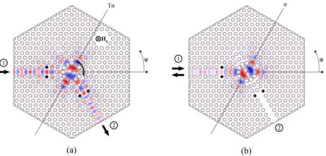
In this work, we consider symmetrical two-ports (shown schematically in Fig.1) that consist of a resona-tor with MO material and two waveguides connected to this resonator. We discuss possible mechanisms of switching by a DC magnetic field H0 in two different geometries of such switches. In the first one, shown sche-matically in Figs.1(a)and1(b), both the input waveguide 1 and the output waveguide 2 are front coupled to the resonator and aligned. In the second switch both wave-guides are side coupled to the resonator. The output waveguide 2, which is parallel to the input waveguide 1, can be oriented in the same direction as the input one or in the opposite direction. In Figs. 1(c) and 1(d) we present the latter case where 180° bending of the output waveguide with respect to the input one can provide more flexibility in design of integrated circuits.
The MO resonator of the two-ports can be magnetized uniformly by a DC magnetic fieldH0in the direction nor-mal to the plane of the two-port x0y (Fig.1).
First, we consider the unloaded nonmagnetic resona-tor, shown schematically in Figs. 2(a)–2(c). The eigen-vectors V1 and V2 with the resonant frequency ω0 corresponding to two orthogonal dipole eigenmodes of the resonator can be written as follows:
V1
1 0
; V2
0 1
: (1)
These two eigenmodes are degenerate [10]. Any combi-nation of them, for exampleV1iV2
V
1
i
; V−
1
−i
; (2)
are also eigenvectors. The last two vectors present rotat-ing in opposite directions eigenmodes with the resonant frequencyω0and they are degenerate as well [Fig.2(c)]. Magnetization of the resonator by a DC magnetic field H0 removes the degeneracy of V and V− [Fig. 2(d)].
a) b)
c) d)
State of switch
on State
of switch
off Standing dipole mode Standing dipole mode Rotating dipole mode 2 2 o 90 H0 1 1 2 2 + x x x x y y y y l l H0 1 1 o 60
Fig. 1. Two-port switches: (a) and (b) front–front coupling of waveguides and resonator (case 1), (a)onstate, (b)offstate; (c) and (d) side–side coupling (case 2), (c)onstate, (d)offstate. Dotted hexagons enclose resonators, circles showHz
compo-nent of idealized dipole modes,H0is DC magnetic field. 4040 OPTICS LETTERS / Vol. 38, No. 20 / October 15, 2013
Now, the rotating clockwise and anticlockwise eigenm-odes V
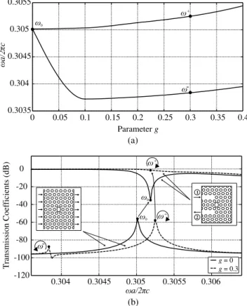
m and V−m have different eigenfrequencies ω andω− [Figs.3(a)and4(a)].
In the nonmagnetic state of the two switches, due to coupling to the waveguides and consequently, lower symmetry, the degeneracy of eigenmodes V1 and V2 of the resonator is removed. Qualitatively, one can expect that the stronger the coupling of the resonator with wave-guides the higher will be the difference between the ei-genfrequencies ofV1 andV2. In the magnetic state, the
coupling of the resonator with waveguides also changes the frequenciesωandω−of the modesV
mandV−m. Be-sides, the quality factorQof the loaded resonator will be lower than that of the unloaded one in both nonmagnetic and magnetic states [see Figs.3(b) and4(b)].
We shall consider separately the two cases shown in Figs. 1(a) and 1(b) (case 1) and Figs. 1(c) and 1(d) (case 2).
Case 1. The excited mode in the nonmagnetic resona-tor isV1[see Fig.2(a)]. From the orientation of dipoleV1, one can see that this mode with the frequency ω0 will correspond to the state on of the switch in Fig. 1(a). In the magnetized resonator, the standing wave with the nodes in the input and output ports will correspond to the stateoffof the switch. Such regime is obtained by the sum of the modes Vm and V−
m with the frequency
ωm≈ωω−∕2[see Fig.1(b)]. Thus, with front–front coupling of waveguides with resonator, in the nonmagne-tized regime the state isonand in the magnetized one the state isoff. One needs to fulfill the requirementsω0≈ωm and rotation of the standing wave due to DC magnetic field by the angle 90° [Fig. 1(b)].
Case 2. In case 2 with side–side coupling, in the non-magnetized regime with properly chosen lengthlwe can have the state off with the standing wave formed by
V2−p3V1∕2[Fig.1(d)], oriented at the angle 60° with respect to the axisy. In the magnetized regime, the state
onis achieved by using one of the rotating modesVmor V−
m[Fig.1(c)]. For functioning the switch, in this case it is necessary to fulfill the requirement ω0≈ω(or ω−).
a) b) c) d) x 2 0 + _ 0 1 + + m m _ _ V V V V V V x x x y y y y 0
Fig. 2. Eigenvectors for nonmagnetized and magnetized un-loaded resonator: (a) dipoleV1oriented alongx, (b) dipoleV2
oriented alongy, (c) two degenerate rotating dipolesVandV− of nonmagnetic state, and (d) two nondegenerate rotating di-polesVmandV−
mof magnetic state.H0is DC magnetic field.
T
ransmission Coef
ficients (dB)
0.3024 0.3028 0.3032 0.3036 0.304
-100 -80 -60 -40 -20 0
g = 0
g = 0.3
1 2
Parameter g
0 0.05 0.1 0.15 0.2 0.25 0.3 0.35 0.4
0.3028 0.303 0.3032 0.3034 0.3036 0.3038 (b) (a) m
Fig. 3. Case 1. (a) Frequency splitting between right- and left-rotating modes of resonator versus tensor parameter g and (b) comparison of frequency characteristics of resonant modes for loaded (right inset) and unloaded (left inset) resonators in nonmagnetized and magnetized PhC.
T
ransmission Coef
ficients (dB)
0.304 0.3045 0.305 0.3055 0.306
-120 -100 -80 -60 -40 -20 0
g = 0
g = 0.3
1
2
Parameter g
0 0.05 0.1 0.15 0.2 0.25 0.3 0.35 0.4
0.3035 0.304 0.3045 0.305 0.3055 (b) (a)
Fig. 4. Case 2. (a) Frequency splitting between right- and left-rotating modes of resonator versus tensor parameter g and (b) comparison of frequency characteristics of resonant modes for loaded (right inset) and unloaded (left inset) resonators in nonmagnetized and magnetized PhC.
Scrutinizing Fig.1, one can see a significant difference in the properties of the two switches. In the component of Figs.1(a)and1(b), DC magnetic field switches off the channel, but in Figs.1(c)and 1(d), on the contrary,H0 switches on the channel.
Notice that in our previous paper [5] devoted to side– front coupled nonsymmetrical switch we erroneously attributed the state on (magnetized resonator) of the switch to a standing wave. A more thorough analysis showed that in fact one of the two rotating modes (ωorω−) is responsible for this regime. Taking the
op-portunity, we thank an anonymous reviewer of our paper [5] who pointed out a possibility to use the rotating modes and indicated paper [11].
In our example, the PhC is a triangular lattice of air holes of radius0.3a(a480nm is the lattice constant) in a magnetic semiconductor. The splitting of the eigen-frequencies of the resonators by the applied magnetic field is shown in Figs.3(a)and4(a).
We have adapted for our purposes the resonator structure suggested in [8]. In order to adjust the reso-nance frequencies inonandoffstates we had to change the geometry of the central hole of the resonator from circular to elliptical. Incase 1, the central elliptical hole of the resonator has the semi-minor axis equal to
0.8475a406.8nm, and semi-major axis equal to
0.8775a421.2nm. Incase 2, it has the semi-minor axis
0.85a408nm and semi-major axis0.95a456nm. In both cases, the radius of the 12 air cylinders of the first ring is 0.38a182.4nm and they form a ring with the radius equal to 760 nm. The 18 air cylinders of the second ring form a ring with the radius equal to 1292.9 nm. The third ring with the radius 1807.2 nm is formed by six air cylinders. The cylinders of the second and the third rings have the radius equal to0.3a144nm. The parameterl [Figs.1(c)and1(d)] is equal to 1047.6 nm.
The guided electromagnetic wave in PhC waveguide is TE mode. The frequency responses of the resonator and the switches were calculated by the software COMSOL [12].
The MO material is described by the following expres-sions for the permittivity and the permeability:
ϵ ϵ0
ϵr −ig 0 ig ϵr 0
0 0 ϵr
!
; μμ0: (3)
(b)
(c) (a)
T
ransmission Coef
ficients (dB)
0.3027 0.3029 0.3031 0.3033
-30 -25 -20 -15 -10 -5 0
off, g = 0.3 on, g = 0
Fig. 5. Switch of Figs.1(a)and1(b). (a) Frequency responses.
Hzdistribution at central frequency: (b) stateonand (c) stateoff.
T
ransmission Coef
ficients (dB)
0.3049 0.3051 0.3053 0.3055
-40 -35 -30 -25 -20 -15 -10 -5 0
off, g = 0 on, g = 0.3
(b)
(c) (a)
Fig. 6. Switch of Figs.1(c)and1(d). (a) Frequency responses.
Hz distribution at central frequency: (b) stateon(arc arrow
In our calculus, we used the values of the parameters
ϵr6.25 andg0.3(information of available parame-ters of the tensorϵone can find, for example, in [13,14]).
In order to exclude the losses in the waveguides (which are at the level of −2÷−3dB) and to consider only the losses of the switch, we calculated first the losses of the nonmagnetized and magnetized waveguide. In the following we subtracted these losses from those calculated for the switch.
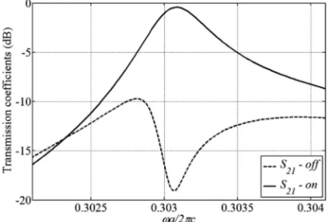
In Fig.5we show the calculated frequency responses and the structure of Hz component of the electromag-netic field of the front–front coupling switch (case 1). One can see that the frequency characteristic in the state
onis defined by the resonance of the modeV1 as it was predicted by our theory [compare with Fig.1(a)]. In the
off state, the frequency band is limited by two rotating modesVm andV−
m of the resonator. Incase 1, the band-width is about 88 GHz at the level of isolation−15dB at wavelength 1.55μm. In case 2 of side–side coupling of switch, the calculated characteristics are given in Fig.6. One can see that in this case we also have the predicted by the above theory behavior of the switch. Incase 2, the bandwidth is about 71 GHz.
Our numerical simulations show that in symmetrical two-ports different mechanisms of switching can be used. The front–front coupled switch without applied DC magnetic field is inonstate and can work as a pass-band filter. When the resonator is magnetized, the switch has the characteristic of a stop-band filter. In side–side coupling, vice versa, the switch with the nonmagnetized
resonator is in the stateoff and behaves as a stop-band filter. With the magnetized resonator, the switch is in the state onand has the characteristic of a passband filter. This work was supported by Brazilian agency CNPq.
References
1. M. Yanik and S. Fan, Appl. Phys. Lett.83, 2739 (2003). 2. A. Sharkawy, S. Shi, and D. W. Prather, Opt. Express10,
1048 (2002).
3. D. M. Beggs, T. P. White, L. Cairns, L. O. Faolain, and T. F. Krauss, IEEE Photon. Technol. Lett.21, 24 (2009). 4. Z. Wu, M. Levy, V. J. Fratello, and A. M. Merzlikin, Appl.
Phys. Lett.96, 051125 (2010).
5. V. Dmitriev, M. Kawakatsu, and G. Portela, Opt. Lett.38, 1016 (2013).
6. V. Dmitriev, M. Kawakatsu, and F. J. M. de Souza, Opt. Lett. 37, 3192 (2012).
7. Z. Wang and S. Fan, Opt. Lett.30, 1989 (2005).
8. W. Smigaj, J. Romero-Vivas, B. Gralak, L. Magdenko, B. Dagens, and M. Vanwolleghem, Opt. Lett.35, 568 (2010). 9. Z. Wang and S. Fan, Photon. Nanostr. Fundam. Appl.4, 132
(2006).
10. S.-H. Kim and Y.-H. Lee, IEEE J. Quantum Electron.39, 1081 (2003).
11. Y. Xu, Y. Li, R. K. Lee, and A. Yariv, Phys. Rev. A62, 7389 (2000).
12.www.comsol.com.
13. M. C. Sekhar, M. R. Singh, S. Basu, and S. Pinnepalli, Opt. Express20, 9624 (2012).
14. E. L. Nagaev, Sov. Phys.-Usp.18, 863 (1975).
20
ARTIGO 3
Magneto-optical resonator switches in two-dimensional
photonic crystals: geometry, symmetry, scattering
Magneto-optical resonator switches in
two-dimensional photonic crystals:
geometry, symmetry, scattering
matrices, and two examples
Victor Dmitriev, Gianni Portela,* and Raphael Batista
Department of Electrical Engineering, Federal University of Para, P.O. Box 8619, Agencia UFPA, CEP 66075-900, Belem, Para, Brazil
*Corresponding author: gianni_portela@hotmail.com
Received 18 February 2014; revised 30 April 2014; accepted 28 May 2014; posted 2 June 2014 (Doc. ID 206529); published 4 July 2014
We discuss different geometrical structures of optical switches based on two-dimensional photonic crys-tals with hexagonal geometry of the unit cell and a magneto-optical resonator. Transition between the statesonandoffin these switches is achieved by an external DC magnetic field. The input and output waveguides can be front–front, side–side, or front–side coupled to the resonator and these different types of coupling can lead to different mechanisms of switching. Analysis of symmetry and scattering matrices of the switches is based on magnetic group theory. Two examples of switches with 60° and 120° bends and their characteristics are also presented. © 2014 Optical Society of America
OCIS codes: (130.4815) Optical switching devices; (230.5298) Photonic crystals.
http://dx.doi.org/10.1364/AO.53.004460
1. Introduction
Different methods can be used to control light in pho-tonic crystals (PhCs). Switches and modulators based on control of light by light, electric field, heat, or DC magnetic field have been suggested recently
[1–4]. In particular, changing some parameters of
magneto-optic (MO) waveguides and resonators by a magnetic field H0, one can switch onand off the light. Three- and four-port circulators of different types [5–7] can also be used as switches if one
changes the sign of the applied DC magnetic field. In our previous papers related to the topic [8,9] we suggested new 2D PhC switches based on an MO res-onator and discussed possible mechanisms of switch-ing. These switches are two-port devices and they have some advantages in comparison to the switches based on circulators. In particular, they have reduced
dimensions and approximately two times smaller time of switching because the external magnetic field is changed from 0 toH0and not from−H0toH0as in case of circulators.
One of the problems of PhC integrated circuits is bending of the waveguides. Even with the small 60° bend of waveguides, the scattering losses of the bend can be significant. For example, optimiza-tion of the 60° bend allowed Frandsen et al.[10] to reduce losses from−8 to −1 dB, but at the expense of a very complex structure of the bend. The switches we developed can simultaneously fulfill the role of 60°, 120°, and even 180° [9] bending elements. Such a diversity of switch geometries can provide a flexi-bility in design of optical integrated circuits.
In this work we discuss the following general topics: geometry and symmetry of switches and cal-culation of their scattering matrices using magnetic group theory. We also present two examples of switches with 60° and 120° bends and their calcu-lated characteristics.
1559-128X/14/204460-08$15.00/0 © 2014 Optical Society of America
2. Possible Geometries of MO Switches in 2D PhCs with a Hexagonal Unit Cell
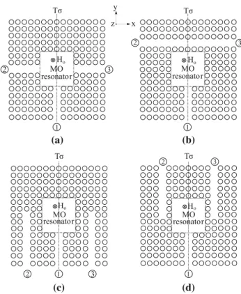
In the first part of our work we shall consider an MO resonator and two waveguides coupled to the resona-tor using the symmetry approach. In Figs. 1–3, we
denote the resonator schematically by a dotted hex-agon without specification of its internal structure. The six-fold rotational symmetry of the hexagon em-phasizes the resonator symmetry. Input waveguide 1 and output waveguide 2 can be front-coupled or side-coupled to the resonator.
Due to the hexagonal geometry of the unit cell of 2D PhCs under consideration, one can consider many possible geometrical variants of the two-ports. Front–front coupled resonators are shown in
Fig.1. Side–side coupling is demonstrated in Fig.2.
Examples of mixed front–side coupling are given
in Fig. 3.
The schemes of Figs.1(c)and2(c)have been inves-tigated in [9], and the possibility to design switch with geometry of Fig. 3(b) has been shown in [8]. Notice that the schemes presented here do not ex-haust all the possible variants.
3. Symmetry Analysis of Scattering Matrices
A. Some Restrictions on Symmetry of the Problem
In the following discussion of possible symmetries we shall exclude from consideration some types of sym-metry. First we shall not discuss the consequences of the periodicity of the crystals, which are mathemati-cally expressed in Bloch’s theorem and geometrically
presented by the Brillouin zone. For nonmagnetic PhCs this can be found, for example, in [11] and for magnetic ones in [12]. Instead, we shall concen-trate on the point group symmetry of the crystals.
The second reduction of the problem complexity is 2D approximation. Though generally any real device or component based on PhCs is three-dimensional (3D), in this paper, we shall consider 2D PhCs described by 2D discrete symmetries, i.e., the sym-metries of plane figures in the planex0y(see Fig.1). The reason for this reduction of dimensionality of the problem is as follows. Two possible elements of sym-metry in a 3D variant corresponding to the third co-ordinatezare the horizontal plane of symmetryz0
and the horizontal axis, for example, thexandyaxis.
(b)
(a) (c)
1 1
1
2 1
2
1 2
2
2 C 2
x y
z
Fig. 1. Examples of front–front coupling of waveguides and resonator and symmetry elements of switches in magnetized and nonmag-netized states: (a) 120° bend, (b) 60° bend, and (c) without bending.
(c)
(e) (f)
(a)
(d)
(b)
1
1
1 1
2 2
1
1
2 C
2
2
2 2
x y
z
Fig. 2. Examples of side–side coupling of waveguides and resonator and symmetry elements of switches in magnetized and nonmagne-tized states: (a), (d), (f) 60° bend, (b) 120° bend, (c) 180° bend, and (e) without bending.
The usual approximation in the analysis of the PhC theory is uniform distribution of the electromagnetic field along the axis z. Thus, instead of the two pos-sible solutions with respect to the third coordinate, namely, the even and odd modes, we can consider only one of them.
The third restriction to the problem is the specific direction of the external DC magnetic field (or magnetization). We choose the direction of uniform magnetization by a DC magnetic field H0, which is perpendicular to the plane x0yof a PhC, i.e., along the axis z. This orientation is typical, for example, for 2D PhC based three-port circulators [5–7]. Such
orientation allows one to consider higher symmetries in comparison to the cases of other possible orienta-tions ofH0. This is because it preserves the two-fold rotational symmetry around the axiszif it exists in the nonmagnetic PhC. All other orientations of the DC magnetic field destroy this rotational symmetry. Besides,H0‖zpreserves the horizontal plane of sym-metry z0 of the nonmagnetic crystal, which is responsible for separation of the eigenmodes as TE and TM [13]. Any other orientation of H0 deletes this plane symmetry and consequently mixes these eigenmodes.
In the following we shall use the Schoenflies nota-tions of magnetic groups [14], whereG,G, andGH are groups of the first (nonmagnetic), second, and third category, respectively.
Symmetry of a two-port depends on symmetry of the PhC, scheme of ports connection, on inner sym-metry of the resonator and symsym-metry of the applied DC magnetic field. In turn, symmetry of the PhC is defined by the symmetry of its materials, geometrical symmetry of its elements, symmetry of unit cells, and the time reversal symmetry (if any).
The resonator can have different formats [5,15–17]. Though its symmetry can be included in
the analysis in the same way as other constituents,
for simplicity we will not discuss details of the geom-etry of the resonator. We assume only that the sym-metry of the resonator is not lower than the symmetry of the other constituents of the problem, i.e., the symmetry of the resonator does not influence the resulting symmetry of the problem.
B. Symmetry of Resonator and Degeneracy of Eigenmodes in Nonmagnetic and Magnetic Regimes
First we consider the unloaded resonator in a non-magnetic regime shown schematically in Fig.4with the symmetry C6v (symmetry of a hexagon). The
standing eigenmodes of our interest are the dipole onesVi(i1;2;…;6). A general form of these modes can be written as follows:
Vi a b : (1)
These modes are highly degenerate. Two of these modes are shown schematically in Fig. 4, namely, with a0; b1 in Fig. 4(a) and a
1∕2; b
3
p
∕2in Fig.4(b). The arrows in the figures indicate orientation of the dipoles. The other eigenm-odes can be obtained by rotation of these two meigenm-odes by 60° and 120° around the axisz. All of these modes have the same resonant frequency ω0 [18].
(a) (d) (b) (e) (c) (f) 1 1 1 1 1 1 2 2 2 2 2 2 x y z
Fig. 3. Examples of combined front–side coupling of waveguides and resonator: (a), (c), (f) 60° bend, (e) 120° bend, (d) 180° bend, and (b) without bending.
V1 V2
x
(a) (b)
y
z
Fig. 4. Examples of standing eigenmodes in nonmagnetized res-onator with symmetryC6v.
The standing modes can be combined in order to produce two rotating degenerate eigenmodes V andV−:
V
1 i
; V−
1
−i
: (2)
These modes also have the resonant frequency ω0 and rotate in opposite directions [Fig.5(a)]. The de-scription in terms of rotating modes is useful in the magnetic regime of switches.
The MO resonator can be magnetized uniformly by a DC magnetic fieldH0in the directionz, normal to the planex0y. Magnetization of the resonator leads to the magnetic groupC6vC6. The degeneracy of the modes Vi is preserved because the group C6vC6 contains the six-fold rotational symmetry. However, the magnetization removes the degeneracy of V and V−. Now, the rotating clockwise and
anticlock-wise eigenmodesV
mandV−mhave different
frequen-ciesω andω− [see Fig.5(b)].
C. Possible Symmetries of Two-Ports
The input and output waveguides connected to the resonator reduce symmetry of the structure. In non-magnetic states, due to coupling to the waveguides and consequently, lower symmetry (the groups C2v,
C2, and Cs), the degeneracy of eigenmodes Vi of
the unloaded resonator is removed. From the group theoretical point of view, this is because the groups C2v, C2, and Cs have no 2D irreducible
representa-tions and, hence, no degenerate modes. The resonant frequencies ofViwill be denoted asωi. Qualitatively,
one can expect that the stronger the coupling of the resonator with waveguides the higher the difference between the frequenciesωi will be.
In the magnetic regime, the coupling of the resona-tor with waveguides also changes the frequenciesω andω−of the modesVmandV−
m. Besides, the quality
factor Q of the loaded resonator will be lower than that of the unloaded one in both nonmagnetic and magnetic regimes.
We start our analysis of the possible groups of symmetry with the geometry of Fig. 1(c), which corresponds to the highest symmetry. The nonmag-netic two-port has the symmetryC2vwith the
follow-ing elements:e(identity), the plane of symmetry σ1 (the planex0), the plane of symmetryσ2(the plane
y0), the two-fold rotation around the z axis C2, and the time reversal T. In the magnetic regime of
Fig. 1(c), the group is C2vC2 with the elements e,
Tσ1 (the antiplane x0), Tσ2 (the antiplane
y0), andC2. The time reversalT in pure form is absent in this magnetic group. The elements and anti-elements of symmetry are shown in Figs. 1
and 2. For the magnetic regime, they are given in
parentheses.
Now, let us consider the two-ports with lower sym-metry. Three subgroups ofC2vcan be considered. For
the two-ports in Figs.1(a),1(b),2(a)–2(c)in the
non-magnetic regime, the symmetry is Cs with the
ele-ments e, the plane of symmetry σ, and the time reversal T. With an applied DC magnetic field H0, the magnetic group is CsC1 having the elements
eand the antiplaneTσ.
Another possible symmetry is the group C2 [Fig. 2(e)]. In the nonmagnetic regime, the group has the elements e, the axis of symmetry C2, and the time reversal T. In the magnetic regime, the group isC2where the axis of symmetry is preserved but the time reversalT is absent.
Still another possibility can exist in the two-port of
Fig.1(c), where the only element present isσ2Tσ2.
The two other elements, namelyσ1Tσ1andC2C2, are absent. Thus, the group of symmetry of this case is the same as for Figs. 1(a), 1(b) and 2(a)–2(c) but
with different orientation of the plane (antiplane) of symmetry.
Notice that all the two-ports of Fig.3 with front–
side coupling are nonsymmetrical.
D. Calculation of Scattering Matrices
The amplitudes of TE (with components Hz, Ex,
and Ey) incident and reflected waves in two-ports
can be represented by 2D vectors of the magnetic field Hi Hi
z1; H i z2
t and Hr Hr
z1; Hrz2t, respec-tively, where t denotes transposition. They are defined by Bloch waves Hi
zn expjωt−kin·r and
Hr
zn expjωt−krn·r, respectively, where j is the
imaginary unit,Hi
znandHrznare complex amplitudes
of the eigenmodes in the waveguides of the two-port (n1;2), and kn is the corresponding wave vector.
The incident and the reflected waves are related by the 2×2 scattering matrix S as follows:
Hr SHi.
In order to define the structure of the scattering matrixSfollowing from symmetry for the unitary elementsσandC2, we use the commutation relation RS SR. For the anti-unitary oneTσ however, the following relation is valid:RS St
R, wheret denotes transposition. The2×2 matrix representa-tions of the elements σ1, σ2, andC2 are Rσ1, Rσ2,
andRC2, respectively:
Rσ1
1 0
0 1
; Rσ2 RC2
0 1
1 0
: (3)
The calculated scattering matrices for the groups C2v andC2vC2[Fig.1(c)] are
SC2v
S11 S12
S12 S11
; SC2vC2
S11 S12
S12 S11
; (4) (a) (b) 0 + _ 0 + + m m _ _ V V V V x x y y 0
Fig. 5. Rotating eigenvectors for (a) nonmagnetized and (b) mag-netized resonator.
and for the groupsCsandCsC1[Figs.1(a),1(b)and 2(a)–2(c)]
SCs
S11 S12
S12 S11
; SCsC1
S11 S12
S21 S11
:
(5) For the groupsC2andC2, the calculated matrices are
SC2
S11 S12
S12 S11
; SC2
S11 S12
S21 S11
: (6)
Finally, for the groupsCs and CsC1[Fig. 1(c), the group elements σ2Tσ2]
SCs
S11 S12
S12 S22
; SCsC1
S11 S12
S12 S22
:
(7) Notice that the elements of matrices (4)–(7),
obtained by symmetry constraints, are frequency independent.
Due to symmetry, the number of independent com-plex parameters of the matrices is reduced from four to three or even two. The matrices in the first column of (4)–(7), corresponding to nonmagnetic regime,
are symmetrical (S21S12), i.e., the corresponding two-ports are reciprocal. The matrices of the second column of (5) and (6) are nonsymmetrical, i.e., the corresponding two-ports are nonreciprocal. However, the matrices of (4) and (7) are symmetrical, i.e., in spite of magnetic regime, these two-ports are recip-rocal. The reflection coefficients from port 1 and port 2 are equal (S22S11) for the matrices (4)–(6), but they are different for the matrices (7). Thus, the presence of the antiplane of symmetry Tσ2 in this two-port leads only to equality of the transmission coefficients S21S12.
4. Photonic Crystal and MO Resonator
The switches discussed below are based on a 2D PhC with the lattice constantain the planex0y. The crys-tal is a triangular lattice of air holes of radius0.3ain an MO material. In the nonmagnetized regime, the material of the resonator is described by the scalar relative permittivity ϵr6.25 and the scalar
per-meability μ0. In the magnetized regime, the MO material of the resonator is characterized by the per-meability μ0 and the following permittivity tensor
ϵ ϵ0 0
@
ϵr −ig 0
ig ϵr 0
0 0 ϵr
1
A; (8)
whereϵr6.25,g0for nonmagnetic regime. Some
examples of materials with magnetic properties that can be used in our switches are given in [19–22].
Using the free software MPB (MIT Photonic-Bands) [23], we have calculated the band diagram
of the PhC (Fig. 6). The TE photonic bandgap corresponds to the normalized frequenciesωa∕2πc
0.285–0.35.
For our purposes we adapted the resonator struc-ture suggested in [5] shown in Figs.11and14. The main parameter for adjusting the resonator fre-quency is the radius of the central hole r0. Using the commercial software COMSOL [24], we have calculated the change in frequency of the localized dipole mode in the nonmagnetized nonloaded resona-tor with respect tor0 (Fig.7). One can see that this parameter can be effectively used in the project of switch synthesis. In the magnetized nonloaded resonator, the splitting of the rotating modes V and V− (see Section 3.B) with respect to the tensor
parameter gis shown in Fig.8.
5. Examples of Switches with 60°and 120°Bending Two new compact optical switches based on a 2D PhC and a magneto-optical cavity are suggested and analyzed below. The resonator is front coupled to two PhC waveguides and operates with a dipole
0 0.10 0.20 0.30 0.40 0.50
TE Photonic Bandgap
Fig. 6. First and second TE frequency bands for nonmagnetized PhC.
r0 /a
0.7 0.8 0.9 1 1.1 1.2
0.28 0.30 0.32 0.34 0.36
TE Photonic Bandgap
Fig. 7. Resonant frequency of dipole mode versus radiusr0of resonator central hole.
g
0 0.1 0.2
0.3029 0.3031 0.3033 0.3035 0.3 +
-Fig. 8. Frequency splitting of dipole modes excited in an MO resonator,r00.8625a.