JOURNAL OF NANO- AND ELECTRONIC PHYSICS Р А А - А Р
Vol. 8 No 1, 01001(4pp) (2016) Том 8 № 1, 01001(4cc) (2016)
2077-6772/2016/8(1)01001(4) 01001-1 2016 Sumy State University
Temperature Dependent IR-Drop Analysis in Graphene Nanoribbon Based Power Interconnect
S. Bhattacharya1,*, D. Das2, H. Rahaman1
1 School of VLSI Technology, Indian Institute of Engineering Science and Technology, Shibpur, India
2 Dept. of Electronics and Communication Engineering, Assam University, Silchar, India
(Received 26 December 2015; revised manuscript received 03 March 2016; published online 15 March 2016)
The paper proposes a temperature dependent resistive model of graphene nanoribbon (GNR) based power interconnects. Using the proposed model, IR-drop analysis for 16nm technology node latest by ITRS is performed. For a temperature range from 150 K to 450 K, the variation of resistance of GNR intercon-nect is ~ 2-5 times lesser than that of traditional copper based power interconnects. Our analysis shows that GNR based power interconnects can show ~ 2-3 times reduction in Peak IR-drop as compared with copper based interconnects for local, intermediate and global interconnects.
Keywords: Graphene nanoribbon (GNR), Temperature, Peak-IR-Drop, Effective-MFP (mean free path), Interconnect.
DOI: 10.21272/jnep.8(1).01001 PACS numbers: 81.05.Uw, 63.22.Np,
61.46.Np.
1. INTRODUCTION
IR-drop has been one of most important challenges of power interconnect in sub-nanometer design [1]. It becomes even more challenging for the high density and high performance designs in which it has adverse effects on timing. The increase in chip operating tem-perature has two-fold effects on timing. Firstly, it creases the interconnect resistance which in turn in-creases the interconnect delay. Secondly, due to the increase in resistance there is more IR-drop which also increases the gate delay. Therefore, it is very essential to analyze the effects of temperature on IR-drop in sub nanometer designs, since the resistivity of the tradi-tional copper based interconnects increases significant-ly in nanometer dimensions [2]. GNR is one of the most promising materials for interconnect modeling for fu-ture generation technologies [2, 3] due to its excellent properties compared with copper in nanometer dimen-sions. Recent studies [3-9] on GNR show its superiority over the traditional copper based interconnect. Howev-er, to the best of our knowledge no investigation has been performed to analyze the effects of the tempera-ture on IR-drop in GNR interconnect. In this paper, we have proposed a resistive model of graphene nanorib-bon (GNR) power interconnect, which is dependent on temperature. Using the proposed model, we have ana-lyzed the IR-drop in GNR based power interconnects. The rest of the paper is organized as follows. Section-II presents the proposed temperature dependent resistive model of GNR interconnect. The results of IR-drop analysis and conclusions are presented in the Sections-III and IV, respectively.
2. TEMPERATURE DEPENDENT RESISTANCE MODEL OF GNR INTERCONNECTS
Due to the presence of large quantum resistance of a monolayer-GNR, a multilayer-GNR structure is pro-posed for modeling nanointerconnect to utilize the long
mean free path as depicted in Fig. 1a. Here, width, thickness, height of multilayer-GNR structure are rep-resented by w, t, ht. The separation between two multi-layer GNR structures is sp. We have considered w 16 nm and t 32 nm for 16 nm ITRS technology node [2]. Fig. 1b shows the 2D-honeycomb lattice struc-ture of single layer-GNR.
Fig. 1– Tri-interconnect model of multilayer-GNR structure (a) and2D honeycomb lattice structure of single layer-GNR (b)
Total number of layers in the multilayer GNR intercon-nect is reported in as [4]
a
S. BHATTACHARYA,D. DAS,H. RAHAMAN J.NANO-ELECTRON.PHYS. 8, 01001 (2016) 01001-2 1 layer t N Integer
(1)
The spacing (δ) between two graphene layers is 0.34 nm which is known as van der walls gap [7]. Using (1) we obtain the number of layers as Nlayer 95 for 16 nm tech-nology node. The total resistance of MLGNR (multilayer graphene nanoribbon) interconnect is given by [7].
(1 MLGNR) Total MLGNR Q
effective l
R R
(2)
where lMLGNR is the length of MLGNR based intercon-nect and λeffective is effective-MFP of MLGNR. Here, ef-fective-MFP is a function of temperature which is mod-eled in this section. The quantum resistance (RQ) is expressed as [4]
2 2. . Q ch layer h e R N N 12.94 . ch layer k N N
(3)
In (3) Nch is the total numbers of conducting channels in monolayer-GNR, Nlayer is the number of layers pre-sent in multilayer GNR, h is Planck’s constant, and e is charge of an electron. The total conducting channels present in monolayer-GNR is expressed in [7].
, ,
( ) ( )
1 1
1 1
[1 ] [1 ]
i n Fe Fe i h
C V
B B
E E E E
n n
k T k T
ch
i i
N e e
(4)where ‘i’ is a positive integer variable, EFe is Fermi-energy, T is room temperature, kB is Boltzmann’s con-stant, nc and nv are known as total number of conduc-tion and valance sub-bands. Here, Ei,nand Ei,h are elec-tron and hole energy for ithsub-band as expressed as [7]
2 F i ihv E w (5)
The total number of channels (Nch) in metallic GNR is equal to 6 [4-5, 7]. The effective MFP of each layer of GNR depends on three important parameters: electron scattering (e), acoustic phonon scattering (ap) and remote interfacial phonon scattering (rip). Electron scattering does not depend on the temperature, but the other two parameters vary with temperature. The elec-tron scattering e can be expressed as [8]
1
( ) 1 ch N ch e defect a N w a
(6)Here, defect is a special kind of MFP of graphene. This MFP is due to the defects present in graphene. The value of defect is assumed to be 1µm [8]. The acous-tic phonon scattering (ap) is expressed as [8]
2 2 2
2 2 s s f ap
A B
h v v w
D k T
(7)
In (7), vf is the Fermi velocity of GNR
( 8 105 m/s),
s
v is the sound velocity of GNR ( 2.1 104 m/s), D
A is deformation potential due to
acoustic phonon, kB is Boltzmann constants, s is 2D mass density in graphene, andTis known as room tem-perature. The remote interfacial phonon scattering can be expressed as [8]
0 1.02 ( 1)
E kT rip EF W e
(8)
Here, is the fitting parameter, EF is the Fermi po-tential ( 0.2 eV), and E0 104 mV. The temperature
dependent effective MFP of GNR is given by applying Matthiessen's rule [4]
1 effective
1 1 1
e ap rip
(9)
Substituting the effective MFP of MLGNR in (2) we obtain the temperature dependent resistance of MLGNR.
3. RESULTS
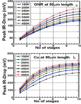
Using the temperature dependent resistance model as discussed in previous section, we have calculated the resistance for different interconnect length and different temperature. In Fig. 2 we have shown the temperature dependent resistance of GNR and Cu interconnect for different interconnect length (5 m to 50 m) for 16 nm technology node. GNR shows ~ 2-5 less resistance than thatof Cu as shown in Fig. 2. With the increase in tem-perature, the effective mean free path reduces, and hence the scattering induced ohomic part of the total resistance of GNR increases. The IR-drop analysis is performed in GNR and Cu interconnects for 5 m (local), 20 m (inter-mediate) and 50 m (global) interconnect lengths. The analysis is per-formed using equivalent circuit model shown in Fig. 3 [9]. In Fig. 3, ten identical CMOS invert-ers are connected in series with temperature dependent resistance for both GNR and Cu. In our analysis, we have assumed the supply voltage as 0.7 V, the input-pulse switches from 0 to 0.7 V for all stages and input-pulse rise and fall time is considered as 100 ps.
TEMPERATURE DEPENDENT IR-DROP ANALYSIS… J.NANO-ELECTRON.PHYS. 8, 01001 (2016)
01001-3 ~ 2-3 less Peak IR-drop than Cu at local, intermediate and global lengths.
Fig. 2 –Resistance vs. temperature plot for GNR and Cu interconnect at 16 nm technology
Fig. 3– Schematic circuit used for power supply voltage drop analysis
Fig. 4 –Peak IR-drop vs. No of Stages at different tempera-ture for 5 m length for GNR interconnect (local level inter-connect) (a) and peak IR-drop vs. No of Stages at different temperature for 5 m length for Cu interconnect (local level interconnect) (b)
Fig. 5 –Peak IR-drop vs. No of Stages at different tempera-ture for 20 m length for GNR interconnect (intermediate level interconnect) and peak IR-drop vs. No of Stages at differ-ent temperature for 20 m length for Cu interconnect (interme-diate level interconnect) (b)
Fig. 6 –Peak IR-drop vs. No of Stages at different tempera-ture for 50 m length for GNR interconnect (global level inter-connect) (a) and peak IR-drop vs. No of Stages at different tem-perature for 50 m length for Cu interconnect (global level in-terconnect) (b)
Table 1 –16 nm PTM CMOS Model Parameters
Model Parameters [10] n-MOS (Si) p-MOS (Si)
Channel Length (L) 16 nm
Channel Width (W) 64 nm 128 nm
Threshold Voltage(VTH0) 0.47 volt – 0.43 volt
Dielectric Constant (ɛox for SiO2)
ɛox 3.9ɛ0,
Where ɛ0 8.85 10– 12 F/m
Oxide Thickness(tox) 0.95 nm 1 nm
Gate Oxide Capacitance (Cox) 0.29 fF 0.28 fF
Junction Depth(Xj) 5 nm
a
b
a
b
a
S. BHATTACHARYA,D. DAS,H. RAHAMAN J.NANO-ELECTRON.PHYS. 8, 01001 (2016)
01001-4 4. CONCLUSIONS
In this work, we have presented a temperature de-pendent resistive model of GNR interconnect and ana-lyzed the effect of temperature on power supply voltage drop (IR-drop). It is observed that with the increase in temperature, the resistance is increased for both GNR and Cu, but GNR shows significantly less increase than the Cu interconnects (~ 2-5 times lesser), which ex-hibits less power supply voltage variation and hence
less impact on the timing of the circuits. It also reduces the power dissipation of GNR based power intercon-nects as compared with Cu.
AKNOWLEDGEMENTS
This work is partially supported by the DIT, Gov-ernment of West Bengal, India under VLSI Design Pro-ject.
REFERENCES
1. A. Vijayakumar, V.C. Patil, G. Paladugu, S. Kundu, 15th International Symposium on Quality Electronic Design (ISQED), 731 (3-5 March, Santa Clara, CA, 2014). 2. International technology roadmap for semiconductors
[ITRS-(2007)].
3. A. Naeemi, J.D. Meindl, IITC-2008, 183 (2008).
4. Azad Naeemi, J.D. Meindl, IEEE T. Electron Dev.56 No 9, 1822 (2009).
5. A. Naeemi, J.D. Meindl, IEEE Electron Dev. Lett.28 No 5, 428 (2007).
6. Chuan Xu, Hong Li, Kaustav Banerjee, IEEE T. Electron
Dev.56 No 8, 1567 (2009).
7. Saeed Haji Nasiri, Mohammad Kazem Moravvej-Farshi,
Rahim Faez, IEEE Electron Dev. Lett. 31 No 12, 1458
(2010).
8. S. Tanachutiwat, Shuhong Liu, R. Geer, Wei Wang, IEEE
International Symposium on Circuits and Systems, 589
(2009).
9. D. Das, H. Rahaman, 5th International Conference on
Computers and Devices for Communication (CODEC), 1 (2012).
![Fig. 1 – Tri-interconnect model of multilayer-GNR structure (a) and 2D honeycomb lattice structure of single layer-GNR (b) Total number of layers in the multilayer GNR intercon-nect is reported in as [4]](https://thumb-eu.123doks.com/thumbv2/123dok_br/17207875.243203/1.892.478.797.603.1011/interconnect-multilayer-structure-honeycomb-structure-multilayer-intercon-reported.webp)