Rodrigo da Silva Mendes Fraústo
Licenciado em Ciências da Engenharia Electrotécnica e de Computadores
RF CMOS Transmitter Front-end with Output
Power Combiner
Dissertação para obtenção do Grau de Mestre em
Engenharia Electrotécnica e de Computadores
Orientador: Prof. Dr. João Pedro Abreu de Oliveira, Prof. Auxiliar, Universidade Nova de Lisboa
Júri
Presidente: Prof. Dr. Rodolfo Alexandre Duarte Oliveira Arguente: Prof. Dr. Luís Augusto Bica Gomes de Oliveira
RF CMOS Transmitter Front-end with Output Power Combiner
Copyright © Rodrigo da Silva Mendes Fraústo, Faculty of Sciences and Technology, NOVA University of Lisbon.
Ac k n o w l e d g e m e n t s
Gostaria de começar por agradecer à Faculdade de Ciências e Tecnologia da Universidade Nova de Lisboa e ao meu orientador Prof. João Pedro Oliveira, por toda a aprendiza-gem, quer a nível académico, quer a nível pessoal. Estas competências adquiridas serão certamente de extrema importância para o meu futuro profissional.
Queria agradecer também a todos aqueles que me acompanharam nesta jornada académica, que tantas voltas teve, tanto pela positiva como pela negativa. A todos eles família e amigos o meu maior agradecimento por terem sido a minha base de suporte e me terem apoiado nos bons e maus momentos.
A b s t r a c t
In this thesis strategies to achieve a high efficiency RF front-end are studied and presented.
A high efficiency Power Amplifier is also proposed and simulated.
The applications for this type of designs are vast, but the main ones are in mobile transmission devices where the only power supply source available is a battery.
In order to perform this thesis several topologies of power amplifiers were studied, and the decision fell to those based on a switching behavior. The reason for this decision was the need for high efficiency (it’s one of the main objectives).
The Class-D power amplifier with its ideal potential efficiency of 100% has proven
the most promising for implementation. The objectives for this thesis in terms of imple-mentation were an efficiency of 20% and an output power of 0dBm.
Finally, a power-combining technique was used to explore the potential of achieving high output power without affecting the efficiency.
Keywords: Class-D, RF power amplifier, CMOS, drain efficiency, radio-frequency,
R e s u m o
Esta tese tem por objectivo o design de um RF front-end de alta eficiência. As utiliza-ções deste tipo de sistemas são vastas, mas as principais incidem sobre dispositivos de transmissão móveis onde a única fonte de alimentação disponível é uma bateria.
Para a realização desta tese diversas topologias de amplificadores de potência foram estudadas, sendo que a decisão tomada foi para as que se apresentam como classes comu-tadas, visto a alta eficiência ser um dos objectivos.
O amplificador de potência Classe-D com a sua ideal eficiência de 100% apresentou-se como o mais promissor para implementação. Os objectivos pretendidos eram de uma eficiência de 20% e uma potência de saída de 0dBm.
Por fim uma técnica de combinação de potência foi utilizada para explorar as potenci-alidades de conseguir uma alta potência de saída sem afectar em demasia a eficiência.
C o n t e n t s
List of Figures xv
List of Tables xvii
Acronyms xix
1 Introduction 1
1.1 Background and Motivation . . . 1
1.2 Thesis Organization . . . 2
2 Units of measurement and Strategies to achieve high power output CMOS PAs 3 2.1 Amplifier Efficiency . . . . 3
2.2 Output Power . . . 4
2.3 Strategies to achieve high power output CMOS PAs . . . 5
2.3.1 Increase Supply Voltage . . . 5
2.3.2 Power combining . . . 6
2.3.2.1 Differential PA architecture . . . . 6
2.3.2.2 On-Chip Transformers . . . 6
3 RF transmission an Overview 9 3.1 Transmitter Architectures . . . 9
3.1.1 Heterodyne Transmitter . . . 10
3.1.2 Direct-Conversion Transmitter . . . 10
3.2 Power Amplifiers . . . 12
3.2.1 Linear Amplifiers . . . 13
3.2.1.1 Class-A Amplifier . . . 14
3.2.1.2 Class-B Amplifier . . . 14
3.2.1.3 Class-AB and C amplifiers. . . 15
3.2.2 Non-Linear Amplifiers . . . 16
3.2.2.1 Class-E Amplifier. . . 19
3.2.2.2 Class-F Amplifier. . . 21
CO N T E N T S
4.1 MOSFET transistor working as a Switch . . . 24
4.2 The CMOS Inverter . . . 25
4.3 The inverter based Class D Voltage-Switching Power Amplifier . . . 26
4.3.1 Principle of operation. . . 29
4.3.2 Ideal analysis . . . 30
4.3.3 Non Ideal analysis. . . 32
4.4 Gate driving . . . 33
4.5 Resonant circuit . . . 34
4.6 Integrated transformer . . . 35
5 Inverter-Based Class-D Power amplifier with power combiner, Design and simulation 39 5.1 Inverter based Class D power amplifier - Design . . . 39
5.2 Inverter based Class D power amplifier - Simulation . . . 42
5.3 Inverter based Class D power amplifier with power combiner - Simulation 45 6 Conclusion and Future work 51 6.1 Conclusion . . . 51
6.2 Future Work . . . 52
Bibliography 55
L i s t o f F i g u r e s
2.1 Voltage-mode transformer. . . 7
3.1 Heterodyne transmitter propose architecture. . . 10
3.2 Schematic of an exemplification of mixing process with a bypass filter before the PA. [10] . . . 11
3.3 Direct-Conversion Transmitter propose architecture. . . 11
3.4 (a) Conceptual oscillator with aφ0phase shift. (b) Open-loop bode diagram, representing the effect of a phase injection. Based on [11]. . . . . 12
3.5 Power amplifiers according linearity of each class. . . 13
3.6 Simplified circuit for current source mode CMOS PAs. . . 13
3.7 Class-A amplifier drain current waveform for two periods. . . 15
3.8 Class-B amplifier drain current waveform for two periods. . . 16
3.9 Class-C amplifier drain current waveform for two periods. . . 17
3.10 Comparison between linear classes drain efficiency. . . . . 17
3.11 Starting point configuration for the understanding of the ideal switching am-plifier. . . 18
3.12 Class-E amplifier. . . 20
3.13 Class-E amplifier dumped network time response. . . 21
3.14 Class-F amplifier. . . 21
4.1 Transistor zones regardingiD versusvDS.. . . 25
4.2 The MOSFET inverter circuit. . . 26
4.3 The first circuit represents the high side, were the NMOS will be conducting, and the second one the low side were the PMOS will be conducting. . . 26
4.4 The first circuit represents the high side, were the NMOS will be conducting, and the second one the low side were the PMOS will be conducting. . . 27
4.5 Voltage-Switching Inverter based Class-D PA. . . 27
4.6 Current-Switching Inverter based Class-D PA. . . 28
4.7 Operation waveform for the voltage switching class D PA at fundamental frequency. . . 30
4.8 Equivalent circuit when on of the transistors is "on". . . 32
4.9 Buffer based power amplifier driver. . . . . 34
L i s t o f F i g u r e s
4.11 1-to-1 transformer taken from [10, pg.821]. . . 36
4.12 Transformer model equivalent adapted from [10]. . . 37
5.1 High-Level implemented architecture for the inverter based Class D power amplifier. . . 40
5.2 Evolution of the PMOS transistor in relation with the channel width ( 4.3). . 40
5.3 The first and second graphic represent the current and voltage at the PA out-put. The last image is theIDC supplied to the PA. . . 43
5.4 PA without driver Output power. . . 43
5.5 The first and second graphic represent the current and voltage at the PA output with the gate driver. The last image is theIDC supplied to the PA and driver. 44 5.6 PA with driver Output power. . . 45
5.7 Two Class D PAs combined. . . 46
5.8 Four Class D PAs combined. . . 46
5.9 Eight Class D PAs combined. . . 47
5.10 Class D PA architecture with power combiner. . . 48
5.11 Class D PA architecture with power combiner. . . 48
L i s t o f Ta b l e s
2.1 Comparison between Power amplifier (PA) classes in terms of peak drain
volt-age and maximum output power [2] . . . 5
3.1 PA power consumption impact in state-of-the-art CMOS transceivers in a va-riety of communications protocols. Adapted from [pg.15] [12] . . . 12
3.2 Conduction angles of the various linear power amplifier class . . . 14
3.3 Power amplifier class F performance overview . . . 22
5.1 Circuit transistors parameters. . . 39
5.2 Resonant circuit parameters . . . 41
5.3 Transistors size and resistance . . . 41
5.4 Transistors size and resistance . . . 44
Ac r o n y m s
BLE Bluetooth low energy.
DAC Digital to analog converter.
PA Power amplifier.
PAE Power Added Efficiency.
C
h
a
p
t
e
r
1
I n t r o d u c t i o n
1.1 Background and Motivation
With the evolution of times, communication has become essential in our lives and tech-nologies. Whether in the way we communicate with each other, using increasingly com-petent mobile devices, or in the way in which the machines and technologies, that are developed, communicate with each other. The need to create a network where multiple devices/machines can communicate with each other, make decisions together or collect data without the need for complex installations has become evident, for example, we can look at the next industrial revolution (industry 4.0) where cybernetic systems create a virtual representation of the real world in order to make decisions in real time and to be totally modular. This allows to look at this type of systems without seeing them as a single unit, but as a set of modules that form an end product.
Another example of the need for wireless communication is in IoT where common everyday devices can communicate and connect to the Internet, making them more pro-ductive and effective.
Taking into account these factors, another concept that became essential, due to the reduced dimensions of many devices and the need for autonomy, was the low power consumption without affecting the functionality.
The essential part of a wireless communication is the emission and reception of a signal that contains information. In this thesis the transmission part is addressed. A high efficiency RF front-end propose and design is presented.
The RF front-end is designed to use in an application where low power is supplied but a need for a high output power exists.
C H A P T E R 1 . I N T R O D U C T I O N
1.2 Thesis Organization
The presented thesis is organized in six chapters including the introduction. The thesis organization is as follows:
Chapter 2 - Units of measurement and Strategies to achieve high power output CMOS PAs In this chapter the units of measurement and combining techniques are addressed. The idea behind it is to give a base knowledge to the thesis reader. Watt output power achieving techniques will be also discuss.
Chapter 3 - RF transmission an Overview In chapter 3 many classes of power ampli-fiers are presented. The classes are distributed between two groups and the distinction is made between them. Each class is briefly described. The main features of the RF am-plifiers, as the output power and the efficiency, are described. The most used transmitter
topologies are also presented and described.
Chapter 4 - Inverter-Based Class-D Power amplifier In this chapter the inverter base Class-D amplifier will be presented. The starting point is the CMOS transistor as a switch, then a study of the inverter circuit is made, ending with the fully Class-D description and analysis. Gate driving and power combining transformers are also addressed.
Chapter 5 - Inverter-Based Class-D Power amplifier with power combiner, Design and simulation The chapter 5 is the design and simulation of the proposed amplifier. The results are showed not only with the Class-D working in a standalone application but also with a power combiner.
Chapter 6 - Conclusion and Future work In this chapter the conclusions and future work are presented.
C
h
a
p
t
e
r
2
Un i t s o f m e a s u r e m e n t a n d S t r a t e g i e s t o
a c h i e v e h i g h p o w e r o u t p u t C M O S PA s
This chapter aims at giving some simple context to this thesis in terms of a better under-standing of the measuring units. Efficiency is a term that seems to be obvious, it’s used
in a variety of situations to describe a system behavior in terms of power consumption when in relation to the output power that the system can achieve. When we talk about an RF power amplifier, efficiency has a similar meaning to what we are used to define in
other applications. The only thing that changes is the power amplifier overall efficiency
where this factor is not only calculated using the power supplied to thePAbut also with the input control signal power. This definitions will be discussed in this chapter.
Another important point is the understating of how to achieve high output power. High efficiency doesn’t always mean that a system have a low power consumption. In the
PAcase, we are speaking about an application that in the majority of times is portable (with a battery) so not only the efficiency is important but also the power consumption.
This chapter will also introduce some concepts in how to achieve a high power output without affecting in a major way the efficiency and power consumption of the system.
2.1 Amplifier E
ffi
ciency
When we talk about the efficiency of a power amplifier the easiest way to measure it is to
get the power that is given by thePAto the load and divide this value with the power that is given by the power supply to thePA. This type of measure is called the drain efficiency
and it’s the most common and easy way to denote the efficiency of the power amplifier.
Drain efficiency is defined by the expression 2.1.
η= Pload P(DC)
C H A P T E R 2 . U N I T S O F M E A S U R E M E N T A N D S T R AT E G I E S T O AC H I E V E H I G H P OW E R O U T P U T C M O S PA S
Looking at aPAdesign from any class or application, we see that this type of measure is not really representing the complete system and could lead to a wrong conclusion about the performance in terms of efficiency. So a better way to perform this measure is to take
in count all the parts of the system. The name of this strategy to measure the efficiency
of the PAis called the Power Added Efficiency (PAE). This measure consists in taking into consideration all the parts of the power amplifier, or by other words, not only the power drawn by thePAbut also the power drawn by the driving stages and the difference
between the output power and the input power. The equation that represents thePAEis
2.2.
η= Pload−Pin P(PA)+
∞
X
n=1
P(Dn)
(2.2)
2.2 Output Power
Output Power is an expression that almost characterizes itself in any application where its used. Being this thesis central topic a Power amplifier, the explanation will be centered on what this expression means for RF power amplifiers.
In a simple phrase output power can be defined as the active power delivered by the power amplifier which flows into the antenna [1]. This power is transmitted under the form of a radiated electromagnetic wave. In antenna design, besides the direction and type of waves, the engineer will, in most cases, create the antenna to be resistive at any frequency of interest. That being said, we can easily imagine the antenna as a resistive load (it is common to design antennas with 50ωof impedance, but the reality is that this value is not true in all cases so the calculations will be in a general case). Starting with the basics, we define instant output power as the voltage times current at any given moment, so we can define the total or average output power by equation 2.3.
Po= lim
T→∞
1 T
Z T /2
−T /2
po(t)dt (2.3)
If we define the output voltage as a simple sine wave with the frequencyfcand the period Tc, we get 2.4
Po= 1 Tc
Z Tc/2
−Tc/2
po(t)dt (2.4)
And if we assume the antenna as a resistive load, and define <.> as the time average operator, we can calculate the output power as 2.5
Po=< vout(t)·iout(t)>=< v
2
out(t)>
RL = V 2 o,rms RL (2.5)
beingVo,rms2 defined as 2.6
Vo,rms2 =
q
< vout2 (t)> (2.6)
2 . 3 . S T R AT E G I E S T O AC H I E V E H I G H P OW E R O U T P U T C M O S PA S
This textbook triviality is not always as useful for a power amplifier as it may look, in reality the power amplifier is not only generating power in the fundamental frequencyfc
but also in its harmonics (that’s why in most cases a strategy is implemented to filter all the undesired frequency’s in order to eliminate the not needed power dissipation). This being said, its more useful to define a fundamental average output power 2.7, where we only take in consideration the fundamental frequency.
Po= V
2
o
2RL
(2.7)
beingVo the amplitude of the sinusoidal output voltage of the fundamental frequency.
This value can be obtained from a Fourier Series expansion ofvout(t) [1].
2.3 Strategies to achieve high power output CMOS PAs
When we talk in a high efficiencyPAwe presume a low power consumption. This affi
r-mation is not always true, because efficiency does not mean that a system will have a
low power consumption, it means that regardless of consumption, the system will have a power output with a ratio close to 1 with its input power. We see that, if we need a solu-tion where the system have a low power consumpsolu-tion, but also a high output power need, some kind of strategy has to be implemented. Some strategy’s can be used to perform this task, the next ones are a collection of them.
Table 2.1: Comparison betweenPAclasses in terms of peak drain voltage and maximum output power [2]
Class Peak Fundamental tone Maximum drain voltage peak drain current output power
Linear PAs 2∗V dd 2∗V ddR V dd2R2
Class D V dd V ddR (π2V dd)2
2R
Class E 3.6∗V dd 1.7∗RV dd 0.577R∗V dd2
Class F 8∗V ddπ 8∗πRV dd (π4V dd)2
2R
2.3.1 Increase Supply Voltage
This strategy is the easiest to think about, if we need high output power, then we supply more power at thePAentry. If we look at equation 2.7we see that more voltage supplied will increase the power output capabilities of the device. But we have to remember the technology that we are working with, modern nm-CMOS are limited in the maximum allowed supply voltage [3].
C H A P T E R 2 . U N I T S O F M E A S U R E M E N T A N D S T R AT E G I E S T O AC H I E V E H I G H P OW E R O U T P U T C M O S PA S
peak voltages superior to the supplied voltage, so the device breakdown voltage needs to be (depending on the PA class) two, tree or four times bigger. Also, some margin its needed to prevent a failure in the device in case of voltage output peaks (common in handling or mismatch conditions) [3].
2.3.2 Power combining
Another strategy used to increase the power output without the concerns of a higher supply voltage is to use an old method to solve complex problems, divide and conquer. The idea behind it is, rather than use a "big"PA, why not use low power output, high efficiency PAs combined in order to achieve the watt level power output [6].
2.3.2.1 Differential PA architecture
By increasing the size of the PA output transistor, power will increase also, but the impedance scales equally to lower values turning sometimes impossible to conveniently convert it to 50Ω [3]. We can bypass this issue using a differential architecture. Basically
the signal will be split into two antiphase paths using a balun or transformer, where two similar PA(half-size) blocks are used, and the signal is merged at the power amplifier output using the same technique [3].Thus, if the PA is not differential, in that case the
signal can be directly fed to and from the power amplifier. There will be losses in the slip-merging process, but we still be able to have a gain of output power.
2.3.2.2 On-Chip Transformers
The real solution for big output CMOS PAs reside in one simple strategy, combine the power of n elements using an on-chip transformer [3]. The transformer combination structures are categorized in two principal categories, series-combining transformers (Voltage-mode) 2.1, that combine the AC voltages on the secondary side resulting in a high output power, or in parallel-combining (current mode) [7].
The big advantage of using the series-combining transformer is that the impedance seen by each amplifier isntimes larger than what would be if connected directly to the antenna. This is a very advantageous situation for the driver design.
The advantages of using parallel-combining transformers are less losses on the sec-ondary, and a better signal symmetry (which is also very important in current-mode transformers to avoid a mismatch and consequentially reduction of power output). The problem is that the number of turns with this approach becomes larger on the secondary side, increasing the area and lowering the self-resonance frequency. Two examples can be found in the literature regarding the two strategy’s, for current mode transformers we have Aokiet al.approach [8] , and for voltage-mode transformers we have the A. Afsahi and L. E. Larson approach [9].
2 . 3 . S T R AT E G I E S T O AC H I E V E H I G H P OW E R O U T P U T C M O S PA S
C
h
a
p
t
e
r
3
R F t r a n s m i s s i o n a n O v e r v i e w
At its core this thesis is the application of various concepts in the design of an RF trans-mitter front-end, so it’s very important to understand what is at stake in this task. This chapter has the intention of providing to the reader a better understanding of the theory behind this thesis.
In a first approach it is important to understand the architecture of a transmitter and the difference between direct-conversion transmitters and heterodyne transmitters, not
only in performance but also in design challenges and inherent problems that each one of them has. Also the concept of digital direct-conversion is introduced to give a theoretical basis about the architecture that will be used in this thesis.
The most critical component of the transmitter is also introduced in this chapter, the power amplifier. The various classes of this device will be studied, and most important the advantages of each one, for a better understanding of the decision to use a Class-D amplifier on this thesis.
Another subject that is introduced are strategies for achieving a High Output Power with integrated CMOS PA, for an understanding of the reason to choose a differential
architecture to achieve this specification.
3.1 Transmitter Architectures
C H A P T E R 3 . R F T R A N S M I S S I O N A N OV E RV I E W
wave into another of a different frequency, usually higher. This process can be realized
through several techniques, which include analog mixing, direct digital conversion and a combination of the two.
Using analog mixing up-conversion as an example, the block used to perform this translation is called a Mixer, it uses a multiplication operation between a rectangular wave coming from an oscillator at the desired RF frequency and the wave at the baseband from theDAC.
At the end of the transmitting chain is the element responsible for amplifying the signal in terms of power so that it is transmitted by the antenna. The name of this block is descriptive of its function: power amplifier. The RF transmitter has three main tasks: modulation, up-conversion and power amplification.
3.1.1 Heterodyne Transmitter
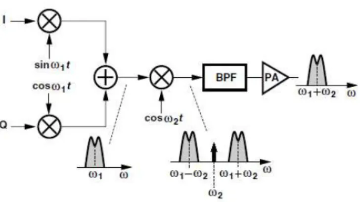
This type of transmitters (Fig.3.1) performs the I/Q up-conversion from the baseband to the desired RF band in two stages. The first one consists in the translation of the baseband signal to an intermediate frequency IF which we callω1. The second stage consists in the
Figure 3.1: Heterodyne transmitter propose architecture.
mixing ofω1with the RF desired frequency (ω2), which will result in two signals, one at
ω1−ω2and another atω1+ω2. Then a bandpass filter will be necessary to eliminate the
first one resulting in the output spectrum that consists in the signal around the RF carrier band (Figure3.2 shows this process). At the end of this transmission chain is a power amplifier that is responsible for the amplification of the output spectrum for transmission at the antenna.
3.1.2 Direct-Conversion Transmitter
Direct-Conversion transmitters are one of the most compact and easy to integrate archi-tectures that can be used. They work by using a quadrature modulator1 to translate the baseband spectrum to the RF carrier band. This implies that this architecture does the modulation and frequency translation in the same place. This block is preceded by a power amplifier responsible for the signal amplification for transmission. Figure 3.3
shows a schematic propose for this architecture.
1Quadrature modulation orQuadrature Phase-shift keying (QPSK)
3 . 1 . T R A N S M I T T E R A R C H I T E C T U R E S
Figure 3.2: Schematic of an exemplification of mixing process with a bypass filter before the PA. [10]
Figure 3.3: Direct-Conversion Transmitter propose architecture.
Despite of being capable to transmit a relatively "clean"signal, or by other words the output spectrum obtained only contains the desired signal around the carrier fre-quency (and its harmonics) without the presence of spurious components, this architec-ture presents some problems that need to be taken into consideration [10]:
• I/Q MismatchIn perfect conditions when quadrature modulation occurs, the I/Q signals should have a difference in amplitude and phase of 90°, but in reality this
is extremely difficult to achieve, resulting in a Mismatch between I and Q signals.
The result of this little big difference results in ”cross-talk” between the quadrature
baseband outputs.
• Oscillator Pulling This effect consists in a ”pulling” of the LO frequency which
happens when there is a frequency that lies out of, but not very far from the lock range2 [11]. Figure3.4(b) shows this effect.
It’s particularly concerning in this topology because the center frequency of the PA output spectrum is equal to the LO oscillation in direct-conversion transmitters. So taking into account that the PA output can exhibit very large swings, which couple to various parts of the system through the silicon substrate, package parasitics, and traces on the printed-circuit board, it is likely that an appreciable fraction of the PA output couples to the local oscillator [10].
2From "Injection locking", that consists in the introducing of a sinusoidal current that forces a phase shift
C H A P T E R 3 . R F T R A N S M I S S I O N A N OV E RV I E W
a b
Figure 3.4: (a) Conceptual oscillator with aφ0phase shift. (b) Open-loop bode diagram,
representing the effect of a phase injection. Based on [11].
3.2 Power Amplifiers
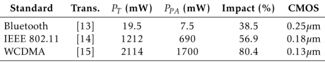
A power amplifier is the key component in the design of a transmitter to use in wireless communication systems. They are characterized for being the most power consumption part of the transmitter, making the decision for an architecture and class critical to the fulfillment of the system requirements. Table 3.1shows the impact of the power amplifier in some of state-of-the-art CMOS transceivers for a variety of communications protocols for a measurable understanding of the importance of this decision.
Table 3.1: PA power consumption impact in state-of-the-art CMOS transceivers in a variety of communications protocols. Adapted from [pg.15] [12]
Standard Trans. PT (mW) PPA(mW) Impact (%) CMOS
Bluetooth [13] 19.5 7.5 38.5 0.25µm
IEEE 802.11 [14] 1212 690 56.9 0.18µm
WCDMA [15] 2114 1700 80.4 0.13µm
Its main purpose is to increase the power level of the signal. Power Amplifiers can be divided in several classes, depending on how the transistor is driven and the harmonic content, or time behavior, of the drain voltage [1]. Another characteristic that defines the various classes of power amplifiers is linear or non-linear working mode. Figure3.5show this exact division of categories according linearity of each class. There are two types of linearity that defines the power amplifier: phase linearity and amplitude linearity. This categorization only defines linearity in amplitude, i.e. a non-linear amplifier has phase linearity. Amplitude linearity is defined by when there is a linear correlation between the output magnitude and the input voltage.
The big advantage of using non-linear amplifiers is the inherent high efficiency of
them, adding that with the fact that more standards and technologies are created that require a low power consumption justifies the main motivation for their wide usage. Several wireless systems and standards use only phase modulation and the corresponding
3 . 2 . P OW E R A M P L I F I E R S
Figure 3.5: Power amplifiers according linearity of each class.
waveforms do not have amplitude variations. As a consequence, the PA only needs to have phase linearity and the amplitude linearity is of no concern. Hence, the non-linear behavior is not considered as a major drawback.
3.2.1 Linear Amplifiers
Looking at figure3.5its visible the various classes according to their amplitude linearity. The linear power amplifier classes are A, B, AB and C. As mentioned before, this group of amplifiers is able to amplify signals with non-constant envelope, such as modulated amplitude signals. All these classes share a common topology, that is, all can be imple-mented using the same base circuit. The main difference between them relates to the bias
voltage at the gate that modifies the current conduction angle [12]. Figure3.6represents this simplified circuit for linear mode CMOS PAs. The parallelLf andCf filter, despite
Figure 3.6: Simplified circuit for current source mode CMOS PAs.
not necessary, it’s been added in order to filter harmonics outside the fundamental fre-quency. This will ensure an improvement in the efficiency of the amplifier, because the
device only affects the load at the fundamental frequency. At all the other frequencies
C H A P T E R 3 . R F T R A N S M I S S I O N A N OV E RV I E W
and has a conduction angle of 360°, through B with a conduction angle of 180°ending in class C which not only has the lowest conduction angle but is also the one that is least linear. It’s also important to define that the non-linearity of the PA have a relation with is efficiency, being class C the most efficient. Table3.2show the conduction angles of the
various linear power amplifier classes[pg.37] [1]. If this amplifier is used with an ampli-Table 3.2: Conduction angles of the various linear power amplifier class
Class Conduction Angle (Degrees)
A 360°(100%)
B 180°(50%)
AB 180°(50%) > and < 360°(100%)
C < 180°(50%)
tude modulated signal, the output voltage Vout will change according to the envelope
signal A(t).
3.2.1.1 Class-A Amplifier
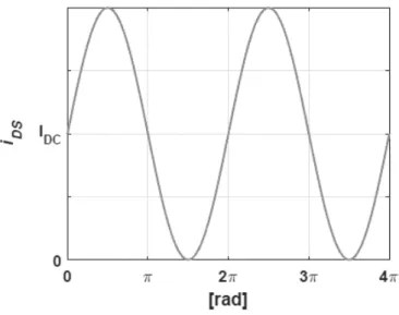
The most inefficient of them all, class A PA are characterized by the in active region
transistor for the entire input cycle(the drain current waveform has a conduction angle of 360°). This creates a necessity for a continuous current consumption that is practi-cally independent from the output power. Drain efficiency, being 50% at its theoretical
maximum, is really poor, especially compared to the other classes. This maximum drain efficiency, assuming that the maximal output swing occurs (Vout=VDC) and whereVout
is the output voltage amplitude, can be calculated as 3.1.
η(%) = 100×Pout PDC =1 2× Vout VDC !2
= 50% (3.1)
However, if we consider, as an example, the use of a class A amplifier in an amplitude modulated signal we see that the output voltageVout will change according to the
enve-lope signal A(t), so if we consider the probability density function of A(t), the efficiency of
the amplifier will fluctuate with it, leading to an average efficiency much lower than the
ideal 50%. Also in equation 3.1we are not taking into account the Knee Voltage3, which will lead to the maximum amplitude of the output voltage being equal to (Vout−VKnee),
resulting in a maximum ideal efficiency of less than 50%. Figure 3.7shows the drain
current waveform for two periods in this class of amplifiers, showing the 360°conducting angle.
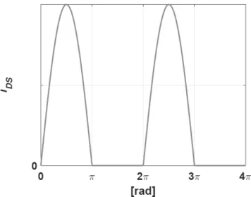
3.2.1.2 Class-B Amplifier
The class-B amplifier like the class-A amplifier is implemented using the same base circuit, but unlike the first one the drain current conduction angle is reduced to 180°,
3The voltage limit that separates the saturation from the triodo region of the transistor output [12].
3 . 2 . P OW E R A M P L I F I E R S
Figure 3.7: Class-A amplifier drain current waveform for two periods.
this is achieved by changing the bias voltage at the gate for this particularly conduction angle. The operation point of the transistor is located exactly at the boundary between the cutoffand the active region [16]. Having half of the conducting angle of the Class-A
PA, its efficiency is greater, but consequently the linearity of the amplifier is degraded.
Equation3.2represents the maximum efficiency theoretical value. If we consider again as
an example, the use of a class B amplifier in an amplitude modulated signal we see that the output voltageVoutwill change according to the envelope signal A(t), so once again
if we consider the probability density function of A(t), the efficiency of the amplifier will
fluctuate with it.
η(%) = π 4×
Vout
VDC !2
= 78.5% (3.2)
Like in the Class-A amplifier, the maximum efficiency only occurs whenVout is equal
VDC, which leads to an approximated efficiency of 78.5% (ignoring one more time the
Knee Voltage). The drain current waveform is depicted in figure 3.8.
3.2.1.3 Class-AB and C amplifiers
Class-AB Power Amplifiers operates (like the name suggests) between the Class-A and Class-B angle, which settles down between 180 and 360 degrees. This naturally induces that depending on its bias network, this type of amplifier conducts somewhere between 50% and 100% in each cycle [10]. Therefore, the drain efficiency lays somewhere between
the 50% maximum of the Class-A amplifier and the 78.5% of the Class-B. The big advan-tage of this type of power amplifier is that it can achieve a better efficiency than a class-A
C H A P T E R 3 . R F T R A N S M I S S I O N A N OV E RV I E W
Figure 3.8: Class-B amplifier drain current waveform for two periods.
of all the linear amplifiers. Although the efficiency grows when the conduction angle is
lowered, the amplifier becomes less linear because turning offthe transistor increases the
number of higher harmonics generated [1]. Because of this low linearity some authors do not consider the Class-C as part of the linear amplifiers group. In theory, the amplifier efficiency can be arbitrary increased toward 100% by decreasing the conduction angle
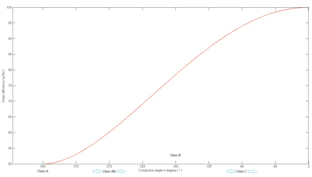
until zero. This has the drawback of also reducing the utilization factor of the amplifier toward zero and increasing the drive power to infinite. The drain current waveform is presented in figure 3.9considering that the LC resonant tank have a high-quality factor, which becomes a short circuit to undesired frequencies besides the fundamental one. The class-AB drain current waveform its not shown because it would be redundant consid-ering the fact that it lies between the Class-A and Class-B waveforms presented before. Figure 3.10(using the expression 3.3valid for all classes addressed) shows a comparison between all linear amplifiers considered in this chapter, regarding their drain efficiency
(maximum theoretical values) versus the particular conduction angle of each one.
η(%) = 1 2×
α−sin(α) 2sin(α2)−αcos(α2)
!
(3.3)
Notice that the Class-AB and C amplifiers have a range of possible values that depend on the conduction angle, as previously mentioned.
3.2.2 Non-Linear Amplifiers
Non-Linear amplifiers are the second group of power amplifiers, they are characterized by the lack of amplitude linearity (it is important to note that they maintain phase linearity). The major reason that makes them interesting is its greater efficiency compared to linear
amplifiers. They achieve this by having a switching behavior, in fact, this behavior gives them a second widely accepted designation, switch-mode amplifiers. If we ignore the
3 . 2 . P OW E R A M P L I F I E R S
Figure 3.9: Class-C amplifier drain current waveform for two periods.
C H A P T E R 3 . R F T R A N S M I S S I O N A N OV E RV I E W
switching losses, ie the transistor is either conducting or closed, or in other words, we have two states, one where the voltage between its terminals is zero and the current passing through them other than zero ("on"state) or the voltage between their terminals is different from zero and the current passing through them is equal to zero ("off"state),
we see that the product of the two, voltage versus current will be always zero, so it’s easy to see that if we consider that these amplifiers don’t have any other losses the efficiency
will be heading towards 100%. Of course in reality the 100 % efficiency value is not
real, but in comparison to linear amplifiers and taking into account their ideal efficiency
values we easily realize the potentiality of this class of amplifiers in a world where power consumption is such an important factor. The class D amplifier, although it is a non-linear amplifier, will be discussed in Chapter 4.
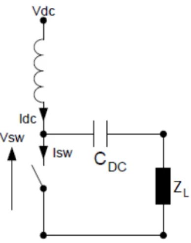
For example, we can take the image 3.11circuit that shows a starting point configu-ration for the understanding of an ideal switching amplifier.
Figure 3.11: Starting point configuration for the understanding of the ideal switching amplifier.
Analyzing this figure we can conclude that the wave produced by this circuit is a square wave with a T period , where theVswwave andIswwave are separated by a phase
of 180°. This suggests a 100% efficiency in the best case possible and only considering
the switching losses, but this is a misconception and it will be demonstrated why.
We know that we are working with square waves so the first step is to calculate the RMS for a square wave with an amplitude of A and a duty cycle of 50%. We do that in
3 . 2 . P OW E R A M P L I F I E R S
equation 3.4.
RMSsquare=
s 1 T ×
Z τ+T
τ
V2(t)dt
= v t 1 T Z T 2 0
A2dt+ 1
T Z T
T
2
(−A)2dt
= s
2A2
T Z T 2 0 1dt =A (3.4)
Now that we have the RMS for a square wave its time to calculate the output of the amplifier in this case. We consider the Fourier series shown in equation 3.5with a period of T.
f(x) = 4 π
∞
X
n=1,3,5,...
1 nsin
nπx
T /2
(3.5)
Having the two components we can thus calculate the expected maximum efficiency of
the switch mechanism for a square wave with a duty cycle of 50 %.
Pf und
Psquare = 4 √ 2π 2 R 12 R = 8
π2 ≈81% (3.6)
This mathematical exercise tells us that no matter how efficient the switch is, the
efficiency is always limited to 81% (this is not entirely true, because we are considering
all the power in a square wave with all the harmonics, if we put a tank circuit in parallel with the load to make a harmonic short, we can reach a theoretical efficiency value of
100%, this will result in a perfect sinusoid at the fundamental frequency being seen by the load), and this is in the most beneficial situation, ie with a duty cycle of 50%, if we reduce the duty cycle we see that this value will be lower. This being said, we will then explore each of the classes in this group of amplifiers.
3.2.2.1 Class-E Amplifier
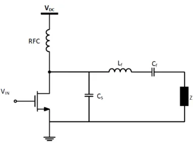
Class-E amplifiers are the most efficient amplifiers known so far [16]. In figure 3.12
is depicted the basic configuration of this type of amplifiers. Like others in class the transistor operates as a switch, and in perfect conditions should turn on and offabruptly.
One of the most attractive feature of this amplifier is that they are designable [17]. The CSis a grounded capacitor that includes the junction capacitance of the transistor and the
parasitic capacitance of the RFC [10], but for high operating frequencies the overall shunt parasitic capacitance is sufficient, makingC
S unnecessary [pag.244] [16]. Values ofCs,
Lf,Cf andZLare chosen in a way that makes the voltage on the source of the transistor
C H A P T E R 3 . R F T R A N S M I S S I O N A N OV E RV I E W
Figure 3.12: Class-E amplifier.
• 1: When the switch is turning off Vt will remain low long enough making the
current drop to zero.
• 2: Vt will achieve zero just before the on state in the switch.
• 3: The derivative ofVt with respect to time is also close to zero as the switch is
turning on.
The first condition solves the issue of finite fall time at the transistor gate. This condition is guaranteed byCs. Without this capacitor,Vt would increase at the same rate thatVin
would drop, allowing the transistor to dissipate power. The second condition exists to ensure the non overlap ofVDS andID near the turn-on point. This will again minimize the power losses in the transistor even with finite input and output transition times. The third condition serves as a protection for violations of the second condition, or by other words, if there is some overlap betweenVDS andID the efficiency degrades only slightly
because when theVt derivative with respect to time is zero it means that at that point
Vt can’t have a significant change near the turn-offpoint [10]. This two last conditions
are less straightforward to achieve, but if we look at figure 3.12we see that when the switch turn offthe load network will operate as a damped second-order system being the
initial conditions define byCs,Lf andCf. The time response of the system depends on
the Q of the network. This is shown in figure 3.13, with an under-damped network, an over-damped network and a critically-damped network response. The last one satisfies the second and third condition because if the switch begins to turn on at this time there is zero slope whenVt approaches to zero volt [10].
This conditions are know as the zero-voltage switching conditions (ZCS).
3 . 2 . P OW E R A M P L I F I E R S
Figure 3.13: Class-E amplifier dumped network time response.
3.2.2.2 Class-F Amplifier
This PA (also called polyharmonic or multiresonant power amplifier) uses one of the oldest methods to improve efficiency [18].
The idea behind it is to let the drain current flow when the drain-to-source voltage is low, and ensure that when the drain-to-source voltage is high the drain current is zero. Therefore, the product of the drain current and the drain-to-source voltage is low, reduc-ing the power dissipation in the transistor and consequently improvreduc-ing the efficiency. In
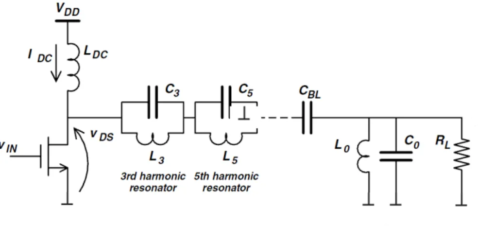
ideal operation the device output will have all even harmonics short circuited (drain cur-rent contains only even harmonics), in order to obtain a half sine-wave curcur-rent waveform, and all odd harmonics open circuited (VDS contains only odd harmonics) to shape the
output voltage to a square wave. This is achieved with lumped-element resonant circuits (or Dielectric resonators). This consequentially defines the input impedance of the load network, for each harmonic frequency, as zero or infinite. In a real usage the class F
Figure 3.14: Class-F amplifier.
will be tuned to multiples of the fundamental frequency, the image 3.14shows a class F amplifier tuned to the third and fifth harmonic (this can be expanded to more multiples, increasing consequentially the efficiency). The table 3.3makes a resume.
C H A P T E R 3 . R F T R A N S M I S S I O N A N OV E RV I E W
Table 3.3: Power amplifier class F performance overview
Classharmonic Peak efficiency
F3 88.4%
F5 92.0%
F∞ 100.0%
can see is that if we use a resonator for all the harmonics we will have, in a theoretical perspective, an efficiency of 100%. This is exactly the reason for the class D power
amplifier selection in this thesis.
C
h
a
p
t
e
r
4
I n v e rt e r- Ba s e d C l a s s - D Po w e r a m p l i f i e r
In this chapter the objective is to explore the architecture used to design the power amplifier. As the name suggests the design is based on a simple CMOS inverter. This chapter will not only explore this circuit but also give the reader a better understanding on class-D power amplifiers and some of its architectures. The class-D PA, as mentioned in another chapter is a switched amplifier (non-linear amplifier).
This type of PA was invented in 1959 by Baxandall [19] and at the time gained the name of class D dc-ac resonant power inverter. Applications are extensive, the most com-mon being audio amplification, solid-state electronic ballasts for fluorescent lamps (were they have one of the most simple and smart circuits), soldering and in any application where a power inverter is needed at a low frequency range.
This type of circuit, has been used for low frequency applications for a long time, but for high frequency applications, such as RF, they have been like ataboo. The reason for that is the switching losses in MOSFET devices at high frequency applications, but with the introduction of even smaller devices, the technology has evolved to a point where hight speed switching is possible, so this highly promising output power PAs are being study again for this type of applications, where big efficiency is needed as well as high
output power.
High output power is extremely difficult to obtain when high efficiency is needed.
C H A P T E R 4 . I N V E R T E R- BA S E D C L A S S - D P OW E R A M P L I F I E R
4.1 MOSFET transistor working as a Switch
As explained in the introduction, for the Class-D PA usability in high frequency appli-cations, high speed switches are needed. The function of a switched PA is dependent of this ON-OFF high speed transition. Lets take a NMOS transistor, the drain current in the linear region is given by the expression4.1.
iD=µn0Cox
W
L (vGS−Vt)− vDS
2
vDS (4.1)
This expression is only valid in the ohmic region (or triode region) of the transistor, which is defined by the conditions in4.2. Theµn0Coxis the transistor intrinsic transconductance
(Kn), µn0 being the low-field electron mobility in the channel and Cox the gate oxide
capacitance per unity area.
vGS> Vt, vDS< vGS−Vt.
(4.2)
TherDS, or the large-signal channel resistance in the same region is given by expression
4.3,
rds=vDS id =
1
KnWL hvGS−Vt−vDS 2
i (4.3)
This expression can be simplified forvDS ≪2(vGS−Vt), gaining the form of 4.4,
rds≈ 1
KnWL [vGS−Vt]
(4.4)
We know also that when the transistor is in saturation region (or active region) the drain current is given by 4.5,
id =1 2Kn
W
L
(vGS−Vt)2 (4.5)
Comparing the previous equations, it’s simple to conclude that for the MOSFET to work as a switch, we need to be in the triode region, so the drain peak current must be sufficiently
lower than the drain saturation current [16]. Image4.1shows the relation between drain current versus drain-source voltage for an ideal MOSFET transistor. It’s also important to refer that in the cutoff state, when the vGS < Vt, the transistor will have a infinite
rds and consequentially the drain current will be zero. We see also that therds in the triode zone 4.3is inversely proportional to the size of the transistor, so if we want a low power dissipation in the transistor, we need to have a high WL relation. This will have another effect on the design, if we look to the gate related parasitic capacitancesCgs and
Cgd expressed by 4.6 (equation in triode region [20]), we see that this increase of size
will make the transistors very difficult to drive because of the high parasitic capacitances
value.
Cgs=Cgd≈Cox
1 2W L+
W Lov
!!
(4.6)
The drive of these high capacitances will be discussed in the next section, because this subject will be very important to achieve a high efficiency.
4 . 2 . T H E C M O S I N V E R T E R
Figure 4.1: Transistor zones regardingiD versusvDS.
4.2 The CMOS Inverter
The inverter is one of the most used circuits in electronics, for example to transfer DC power to AC power. It’s also used as a buffer or a driver in a variety of circuits, or as
the name suggests, to invert the signal. In this last application we can see it applied for example in ring oscillators. Another use for the CMOS inverter is for power amplifica-tion, in the audio area for example, is a long partner in this usage. This low frequency application as seen the inverter as a good way to make a high efficiency output power
stages reducing the heat dissipation and increasing the lifetime of the battery in portable applications [21].
In a simple way the inverter is two switches, one NMOS and another PMOS, with an infinite offresistance (whenv
GS < Vt) and a finite on-resistance when in the linear zone
(whenvGS > Vt) as discussed in the previous section. Image 4.2shows the static circuit
for the CMOS inverter. When we look at this circuit a very intuitive understanding of it can be done. When the input signal is equal to V ddwe will be in the high state of the input. This will cause the NMOS transistor to be "on"creating a direct path between the ground and the Vout. For the low state of the input, when the input signal is zero, the
PMOS will be active connecting the power supply to Vout. The two circuits in 4.3are representative of this input dependent switching. It’s easy to see that in the inverter when the signal input is in the high state the output of the circuit will be in the low state, and when the input signal is at low state the output will be in the high state. This is where the name inverter comes from, the digital "1"is converted to digital "0"and vice versa.
C H A P T E R 4 . I N V E R T E R- BA S E D C L A S S - D P OW E R A M P L I F I E R
Figure 4.2: The MOSFET inverter circuit.
Figure 4.3: The first circuit represents the high side, were the NMOS will be conducting, and the second one the low side were the PMOS will be conducting.
This graphic also shows a zone where both the transistors are saturated, this will cause a direct short from the power supply to ground causing losses and stress on the devices. This type of behavior will be explored in the next chapters.
4.3 The inverter based Class D Voltage-Switching Power
Amplifier
There is two types of class-D amplifiers, the voltage-switching(or voltage-source) and the current-switching (or current-source). In the first type they are power supplied by a voltage source and have a series-resonant circuit at theVout. If the resonant circuit quality
4 . 3 . T H E I N V E R T E R BA S E D C L A S S D VO LTAG E - S W I T C H I N G P OW E R A M P L I F I E R
Figure 4.4: The first circuit represents the high side, were the NMOS will be conducting, and the second one the low side were the PMOS will be conducting.
factor is sufficiently high the current passing through the resonant circuit is a sinusoid
and in the MOSFET switches a half-sine. The drive made to the switches is a square wave. Image 4.5shows a voltage-switching inverter based class D power amplifier base circuit. In the current switched case, current will be supplied (Vdd with an RFC choke), and a
parallel-resonant circuit will be placed before the antenna (the base circuit is showed in image 4.6). The load will see a voltage sinusoidal wave (if again the quality factor is sufficiently high), and the switches half-sinusoid voltage wave [16]. If we look at this
Figure 4.5: Voltage-Switching Inverter based Class-D PA.
C H A P T E R 4 . I N V E R T E R- BA S E D C L A S S - D P OW E R A M P L I F I E R
Figure 4.6: Current-Switching Inverter based Class-D PA.
The first important thing to mention is that cross-conduction will occur causing spikes in the drain current, this is justified by the image 4.4were we can see that during a small period of time both transistors are conducting so we will have a direct short from the power supply to ground, this issue can be minimized if we use non-overlapping gate-to-source voltages to give time for one transistor to be in cutoffzone. In literature we can
find some examples like [23] but this method will increase the complexity of the driver circuit.
The next thing that we see is that this circuit can be seen as two switches working from triode to cutoffzone one at a time. If we look at the condition to be in the transistor
linear zone (equation 4.1) we see that the drain-to-source voltage needs to be smaller then the gate-to-source voltage. So this means that the power supply voltage needs to be relatively small to avoid voltage breakdown of the gate oxideSiO2(one way to avoid
this is to use a voltage mirror driver or a voltage level shifter, again this will increase the driver complexity. We can find some literature examples like [24]). This second issue for RF application is not really relevant, because in this type of application the power supplied voltage is low, due to the need of system portability (supplied voltage is usually a battery).
One of the issues with this architecture as already explained, the oxide breakdown, when the gate-to-source voltage swing is to high. Another issue that is also common in this type of architecture is the hot carriers effect. This effect is particularly visible in
switched architectures because of the constant switching between the on and offstates,
cutoffzone and triode zone. The effect consists in carriers traveling at high speeds in the
transistor channel and colliding with the edges. Because of this high velocity and energy
4 . 3 . T H E I N V E R T E R BA S E D C L A S S D VO LTAG E - S W I T C H I N G P OW E R A M P L I F I E R
collisions, they will create electron-hole pairs by impact ionization. The generated bulk-pair carrier will be collected by the drain or injected into the gate oxide. If the second effect occurs this will lead to hot carrier degradation (like a change of the threshold
voltage due to occupied traps in the oxide). The hot carriers can also generate traps at the silicon-oxide interface (fast surface states). The effects caused by this will be
sub-threshold swing deterioration and drain leakage [25]. A similar phenomenon that in this case can cause a premature degradation of the transistor is the core principal used for energy generation in photovoltaic cells.
4.3.1 Principle of operation
As the name suggests this topology has a similar working principle as the CMOS inverter with one major difference, at the system output a resonant circuit is present, being in the
case of a voltage-switching topology a series-resonant circuit and in the current-switching case a parallel one. The resonant circuit LC is designed to work at a certain frequency (fundamental frequency). If the quality factor is high enough (QL > 2.5) the current
throughout the LC resonant circuit is a sine wave. The quality factor can be calculated by expression 4.7.
QL=
q
L C
R (4.7)
The image 4.7, adapted from [16, pg.170], shows the class-D PA operation waveforms. In the original image we can see that there are three operation conditions, one where the output frequency is lower then the fundamental frequency (the resonant circuit will be seen as an high capacitive impedance), one were the output frequency is equal to the fundamental frequency and a last one were the output frequency is above the fundamen-tal frequency (the resonant circuit will be seen as an high inductive impedance). In real systems we will see these three conditions, but for the propose of this explanation we will only concentrate on the "ideal case", which is the output frequency being equal to the resonant frequency.
The circuitVin is a square wave that goes from 1 to 0, this can be seen in image 4.7as
theVGS andVSG.
When the control input square wave is at the low level the PMOS transistor will be conducting and the NMOS will be at cutoffzone. As the PMOS is conducting the output
of the circuit will be equal to the supplied voltage. A current will start to flow from the supplied voltage to the resonant circuit plus the load at the end. This will create a positive half-sine wave, since the resonant circuit has a high quality factor. Considering that we have no losses at the transistor and this is an ideal case the source-to-drain voltage in the PMOS transistor will be zero. For the other part, when the control square wave is at the high level the NMOS transistor will conduct and the PMOS will be at the cutoff
C H A P T E R 4 . I N V E R T E R- BA S E D C L A S S - D P OW E R A M P L I F I E R
Figure 4.7: Operation waveform for the voltage switching class D PA at fundamental frequency.
as we are considering an ideal case, there will be no losses so theVDSnwill be zero. The
charged series-resonant circuit will force a current in the opposite direction, creating the negative half-sine wave. The charging process of the resonant circuit is simple to explain, the resonant circuit is composed by an inductor(that stores energy, when a current passes through, in a magnetic field) and a capacitor (that accumulates charge in a electric field). When the PMOS is active, power is flowing fromVDC to the LCR circuit, as current is passing through the inductor this will charge the magnetic field. When the PMOS is OFF and the NMOS is ON the charged inductor will dissipate it’s energy, creating the negative current. As the resonant circuit is tunned for the fundamental frequency, this will occur with an oscillating frequency equal to the fundamental frequency.
4.3.2 Ideal analysis
As stated before the image 4.7represents the operation at the fundamental frequency (f0) without any losses. This will serve as base for the ideal analysis of the circuit. If
there is no power being dissipated, and the drain-to-source voltages don’t overlap with the current waveforms no power is dissipated. Also when the switching of the transistors occurs the current at their terminals is zero so we can say that the Zero-current-switching (ZCS) condition is achieved. As stated before the transistors are ideal consequentially the switching action is made at the same frequency as the input control square wave. So we
4 . 3 . T H E I N V E R T E R BA S E D C L A S S D VO LTAG E - S W I T C H I N G P OW E R A M P L I F I E R
can express the drain-to-source voltage as the trigonometric Fourier series for the square wave knowing that between 0 andπthe amplitude will be equal to the supplied voltage and betweenπand 2πthe amplitude will be 0 (assuming the NMOSVDS). Also we ignore
the odd harmonics because we are assuming a perfect square wave function.
VDSn=V dd
1 2+ 2 π ∞ X n=1
1−(−1)n)
2n sin(nwt)
=V dd 1 2+ 2 π ∞ X k=1
sin[2k−1]wt 2k−1
(4.8)
We know that the load quality factor needs to be high for the voltage that crosses the load to be a sinusoid with the tunned resonant circuit frequency. In this ideal case we are assuming this factor. So the output voltage is 4.9.
v=Vmsin(wt) (4.9)
where the amplitudeVm(first harmonic) is given by,
Vm=
2
πVDC (4.10)
and the current i through the load is also a sinusoid,
i=Imsin(wt) (4.11)
The current amplitude is given by,
Im=RVm load = 2 π VDC Rload (4.12)
The current given by the power supply to the circuit is equal to the current passing through the PMOS transistor, so we can conclude that is value its different from zero only
on half of the control cycle (from 0 toπ). Being this period the same that the PMOS is active. In the other half period the PMOS is offand the NMOS is conducting.
Using 4.11we know that the current that passes in the load is a sinusoid, so we can calculate the DC current,
IDC=
1 2π
Z 2π
0
Imsin(wt)dwt=2Imπ
Z π
0
sin(wt)dwt=Im
π =
2VDC
π2R
load
(4.13)
Having the DC current consumption, its easy to get the power requested to the power supply,
PDC =VDCIDC =
2VDC2 π2R
load
(4.14)
Now that we have the input power, in order to calculate the efficiency of the amplifier,
we need to get the power dissipated on the load. We know that the output current is given by 4.12, so the power output is given by,
C H A P T E R 4 . I N V E R T E R- BA S E D C L A S S - D P OW E R A M P L I F I E R
This will bring us to the reason why the class D amplifier is so promising in terms of high efficiency, the theoretical efficiency is 1(4.16)
η= PO
PDC = 1 (4.16)
In a real application this analysis is not valid, for example it’s impossible achieve no losses in the transistors. Nevertheless this is a promising start for the class DPA, as a great power amplifier for radio frequency portable applications where the efficiency and
low consumption are so difficult to achieve. In the next section a more realistic approach
will be used for the same calculations.
4.3.3 Non Ideal analysis
The first thing that needs to be taken into account is the on-resistance of each transistor. This resistance is linear and equal for both transistors,
rDS=rDSp =rDSn (4.17)
We are also assuming that the parasitic capacitances of the transistors are linear, and the elements of the series-resonant circuit are passive, linear and time invariant. The inductor internal resistance will be denoted asrLand the capacitor internal resistancerC.
Looking at the equivalent circuit (4.8) we see that when one of the transistors is "on"and
Figure 4.8: Equivalent circuit when on of the transistors is "on".
the other is "off", we can denote the total resistance of the circuit as 4.18.
Rtotal =rDS+rL+rC+R (4.18)
Since there are two transistors, and they conduct in half period each one, we can denote the equivalent resistance in the linear zone as half,
rDS=
rDSQ+rDSN
2 (4.19)
As stated before the circuit is only draining current from the power supply when the PMOS transistor is on(4.11), so there is a need to calculate the current rms value,
Irms=
s 1 2π
Z 2π
0
(Imsin(wt))2dwt=I2m (4.20)
![Table 2.1: Comparison between PA classes in terms of peak drain voltage and maximum output power [2]](https://thumb-eu.123doks.com/thumbv2/123dok_br/16572156.738065/25.892.198.694.722.907/table-comparison-classes-terms-drain-voltage-maximum-output.webp)