J. Nano- Electron. Phys.
3 (2011) No1, P. 926-936 (Sumy State University) 2011 SumDU
926 PACS 85.30._z, 85.30.De, 85.30.Kk
CURRENT TRANSPORT BEHAVIOUR OF Au/n-GaAs SCHOTTKY DIODES GROWN ON Ge SUBSTRATE WITH DIFFERENT EPITAXIAL
LAYER THICKNESS OVER A WIDE TEMPERATURE RANGE
N. Padha1, R. Sachdeva1, R. Sihotra1, S.B. Krupanidhi2
1 Department of Physics and Electronics,
University of Jammu, Baba Sahib Ambedker Road, Jammu Tawi-180006, India
E-mail: [email protected] 2 Materials Research Center, Indian Institute of Science, Bangalore 560012, India E-mail: [email protected]
The work presents temperature dependent forward and reverse current-voltage (I-V) analyses of n-GaAs/Au Schottky Diodes grown on n+ Ge substrate with different epitaxial layer thicknesses. While some of the Schottky diodes follow TED mechanism, others exceed significantly from this theory due to existence of patches of reduced barrier height embedded in the Schottky interface. The zero bias barrier heights ( bo) increase (0.649 to 0.809 eV) while the ideality factors ( ) decrease (1.514 to 1.052) with increase in epitaxial layer thickness (1-4 m), thus, indicating similar behaviour to that observed for the I-V characteristics of the undertaken Schottky diodes with decreasing temperature. It all indicated the existence of barrier inhomogenities over the M-S interface. The breakdown behaviour analysis of these diodes showed some interesting results; the breakdown voltage (VBR) decreases with temperature and shows ‘Defect Assisted Tunneling’ phenomenon through surface or defect states in the 1 m thick epitaxial layer Schottky diode while VBR increases with temperature in 3 m and 4 m thick epitaxial layer Schottky diodes which demonstrate ‘Avalanche Multiplication’ mechanism responsible for junction breakdown. The reverse breakdown voltage is also seen to increase (2.7-5.9 Volts) with the increase in epitaxial layer thickness of the diodes. The undertaken diodes have been observed to follow TFE mechanism at low temperatures (below 200 K) in which the tunneling current component increases with epitaxial layer thickness which has been ascribed as an impact of GaAs/Ge hetero-interface over the Au/n-GaAs Schottky barrier.
Keywords: IDEALITY FACTOR, BARRIER HEIGHT, THERMIONIC FIELD EMISSION, TUNNELING, INHOMOGENITIES, JUNCTION BREAKDOWN, RICHARDSON CONSTANT.
(Received 04 February 2011)
1. INTRODUCTION
CURRENT TRANSPORT BEHAVIOUR OF Au/n-GaAs… 927
It has now been well established that metal-semiconductor structures especially Schottky contacts play a key role in making new semiconductor devices [1-4]. Due to its technological importance, full understanding of the nature of their electrical characteristics has been explored. It has also been explored that the interface properties of MS contacts show a dominant impact on the device performance, reliability and stability [5]. The interfaces are very complex regions and their behaviour depend on the preparation conditions [6]. It has been reported in some works in the recent past that the barrier height inhomogenity is caused by grain boundaries, defects, existence of multiple phases in the metal-semiconductor interface [7-9]. The presence of small regions of low barrier heights was experimentally evidenced by using Ballistic Electron Emission Spectroscopy (BEES) [10, 11]. Efforts have also been made to describe the anomalies of the conduction mechanism over Schottky barriers by using TFE theory [12]. Work has also been reported regarding the use of GaAs/Ge epitaxial heterostructure interface for the fabrication of space quality Solar Cells [13] wherein Ge behave as an optimized substrate material for high efficiency GaAs/Ge photovoltaic devices. The GaAs/Ge heterostructures are, however, found extremely sensitive to defects. In the present work, an attempt has been made to establish the current transport phenomenon of the Au/n-GaAs Schottky Diodes at different n-GaAs thicknesses grown on n+ Ge substrates as studied over a wide temperature range.
2. EXPERIMENTAL
Schottky Diodes of the type n-GaAs/Au, with different n-GaAs epitaxial layer thicknesses were grown on n+ Ge substrate, mounted on the To-39, package and undertaken for the forward and reverse biased current-voltage (I-V) analyses over a wide temperature range. The room temperature I-V characteristics were measured using an automated arrangement consisting of a Keithley’s Source Meter (Model 2400), an IBM PC (Pentium-IV) and a Probe Station. The To-39 headers were mounted on a Closed-Cycled Liquid He refrigerator (CTI-Cryotronics Model 22CP) equipped with temperature controller (Lake Shore Model 321) for measuring the temperature dependent I-V characteristics. The temperature dependent I-V characteristics of the Schottky Diodes were carried out from room temperature to low temperatures. The temperature was maintained within a step ± 1K during the data acquisition. The carrier concentrations of the grown epitaxial layers were measured using capacitance-voltage (C-V) measurement at 1MHz frequency using HP 4194A LCR Bridge. The carrier concentration was subsequently confirmed by an electrochemical C-V (ECV) profiler measurement setup.
3. RESULTS AND DISCUSSION
3.1 Current-Voltage (I-V) characteristics:
928 N. PADHA, R. SACHDEVA, R. SIHOTRA, S.B. KRUPANIDHI
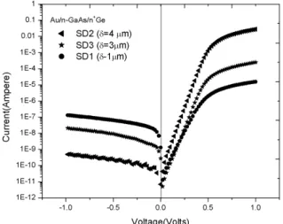
Fig. 1-Room temperature forward and reverse biased current-voltage (I-V)
characteristics of the Au/n-GaAs/n+Ge Schottky Diodes with epitaxial layer
thicknesses of 1mm (SD1), 4mm (SD2) and 3mm (SD3) respectively
The current through a uniform Metal-semiconductor interface is normally considered on the basis of thermionic emission theory expressed as under:
( )
exp S 1
S
q V IR
I I
KT h
é æ - ö ù
= ê ç ÷- ú
è ø
ë û (1)
where IS, the saturation current and JS, the saturation current density
defined as :
** 2exp b0
S S
q
J I S A T
KT
f
æ ö
= = ç- ÷
è ø (2)
The quantities S, A**, T, k, q, fbo and RS are the diode area, the effective
Richardson constant, the temperature in Kelvin, Boltzman’s constant, the electronic charge, the zero bias barrier height and the diode series resistance, respectively. fbo is the effective barrier height determined from IS found from the experimental data of Schottky Diodes. The effective
Richardson constant value of 3 A cm-2K-2 was used for n- GaAs [14]. The ideality factor, is introduced to describe the deviation of the experimental I-V data from the ideal TED model (h = 1 for ideal case). The effective values of ideality factor using equation (1) is given by
(
)
ln S
q dV
KT d I I
h = (3)
CURRENT TRANSPORT BEHAVIOUR OF Au/n-GaAs… 929
thickness. The forward I-V characteristics of the undertaken Schottky Diodes (SD1-SD3) have been measured from room temperature to low temperatures as shown in Fig. 3(a-b). A computer program is utilized to fit the experimental I-V data taking fbo, h and RS as adjustable parameters [15]. The parameters JS,
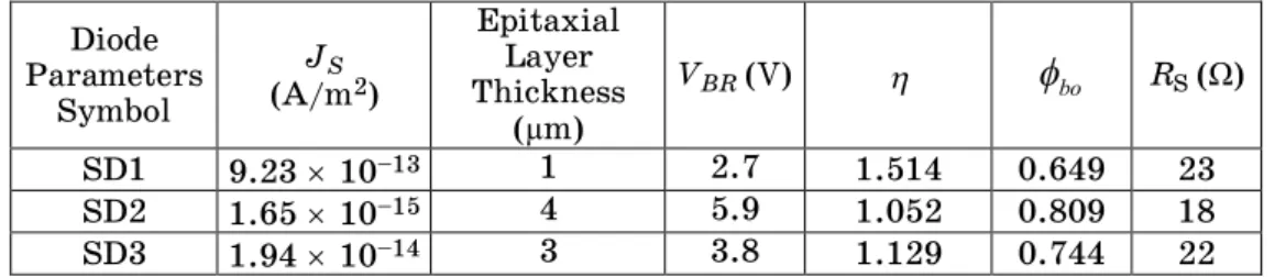
fbo, h and RS measured from the I-V characteristics have been illustrated in Table 1. The values of RS (18-23 Ω) given in Table 1 determined from the fittings are justified since heavily doped substrates been used.
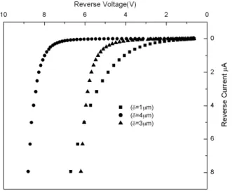
Fig. 2 - Reverse biased I-V Characteristics of three different epitaxial thicknesses in the Au/n-GaAs/n+Ge Schottky diodes measured at room temperature
Fig. 3 - Forward I-V characteristics of n-GaAs/Au Schottky Diodes of and a) 4 µm (SD2) b) 3µm (SD3) at different temperatures (Diode area= 1.25 ´ 10-7m2)
930 N. PADHA, R. SACHDEVA, R. SIHOTRA, S.B. KRUPANIDHI
range at all temperatures. However, in SD3, shown in Figure 3 (b), I-V cha-racteristics show deviations at the current values below 10-8 A. Similar, deviations have also been observed below the current values of 10-6A in SD1 (not shown in the Fig. 3). Referring Fig 3 (b), it is observed that the currents in the small bias region in SD3, exceeds significantly to the predicted TE values, a typical plateau like section has been observed in this case which may be due to the ‘patches’ of reduced barrier heights embedded in the Schottky interface explained on the basis of Tung’s pinch-off model [16].
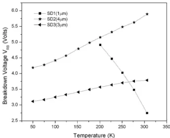
Fig. 4 - Breakdown Voltage VBR vs. Temperature for n-GaAs/Au Schottky diodes
grown on Ge substrate with different epitaxial layer thicknesses
CURRENT TRANSPORT BEHAVIOUR OF Au/n-GaAs… 931
The reverse characteristics of the undertaken Schottky diodes have been plotted in Fig. 2. It is observed that at room temperature, the breakdown voltage (VBR) increases with epitaxial layer thickness as shown in Table. 1.
Further, referring Fig 2, it is observed that the knee point is not well defined and causes ‘soft’ breakdown phenomenon in SD1. However, in case of SD2 and SD3, well-defined knee voltage is observed and thus causes ‘sharp’ breakdown voltages. The reverse breakdown voltage (VBR) verses temperature plots of all Au/n-GaAs/n+Ge Schottky diodes have been plotted in Fig. 4. The breakdown voltage, VBR has been defined as the reverse
voltage at which the current becomes equal to few micro amperes [17].
Table 1 - Au/n-GaAs/n+-Ge Schottky diode parameters at different n-GaAs epitaxial thicknesses measured at room temperature
Diode Parameters
Symbol
JS
(A/m2)
Epitaxial Layer Thickness
(ᖨm)
VBR(V) h
f
bo RS (Ω)SD1 9.23 ´ 10–13 1 2.7 1.514 0.649 23 SD2 1.65 ´ 10–15 4 5.9 1.052 0.809 18 SD3 1.94 ´ 10–14 3 3.8 1.129 0.744 22
Table 2- Schottky interface parameters of SD1-SD3 Schottky Diodes
determined over a wide temperature range
It is observed that the breakdown voltage of SD2 (4 mm) and SD3 (3 mm) are
found to increase linearly with temperature and so the breakdown voltage has positive temperature coefficient which is indicative of ‘Avalanche Multiplication’ mechanism responsible for junction breakdown [18]. However, in case of SD1 (1 mm), the breakdown voltage decreases with temperature and gives negative temperature coefficient which indicates the possible breakdown mechanism as ‘Defect Assisted Tunneling’ through surface or defect states.
T (K)
SD1(1mm thickness) SD2(4mm thickness) SD3(3mm thickness)
h
f
bo RS(Ώ) hf
bo RS(W) hf
bo RS (W)300 1.513 0.649 22 1.052 0.809 18 1.129 0.745 22 275 1.561 0.628 23 1.057 0.811 19 1.167 0.728 22 250 1.59 0.617 26 1.075 0.808 20 1.223 0.714 25 225 1.601 0.608 26 1.115 0.794 18 1.270 0.696 22 200 1.643 0.59 20 1.160 0.775 18 1.370 0.658 18
175 1.213 0.753 16 1.391 0.642 25
150 1.260 0.723 22 1.410 0.623 28
125 1.300 0.705 25 1.690 0.537 25
100 1.533 0.614 24 1.720 0.517 43
75 2.145 0.457 21 2.350 0.393 29
932 N. PADHA, R. SACHDEVA, R. SIHOTRA, S.B. KRUPANIDHI
3.2 Zero-bias barrier height, ideality factor and series resistance
A typical plot of the zero bias barrier heights (fbo) and ideality factors (η)
derived from the fittings of the I-V data of SD1-SD3 Schottky Diodes at various temperatures using equations (1) and (2) has been plotted in Fig. 5. In all the diodes, the zero-bias barrier heights (fbo) decrease and ideality
factors (h) increase with decrease in temperature has been given in Table 2. Referring to Table 1 and 2, it is observed that the zero-bias barrier heights increase and ideality factors decrease with the increase in epitaxial layer thickness, these changes are indicative of deviations of the current transport phenomenon from the pure thermionic emission diffusion (TED) mechanism and there is a current flow, in excess, to that due to the standard thermionic emission diffusion (TED) theory. Similar trend is also observed with increase in temperature of the I-V characteristics measurements. The reason for considerable deviations may be due to the impact of Ge substrate on the n-GaAs semiconductor surface which may cause increased density of states at the semiconductor surface due to surface roughness, imperfections etc. The barrier height can also be determined from ln(JS/T2) versus (1000/T) plot obtained by re-arranging equation (2) in the manner given below :
(
2)
** 0ln b
S
q
J T A
KT f
= - (4)
Therefore, the ln(JS/T2) versus (1/T) plot should be a straight line with the slope yielding the zero bias barrier height (fbo) and the intercept at the
ordinate, the effective Richardson constant (A**). An example of the type of
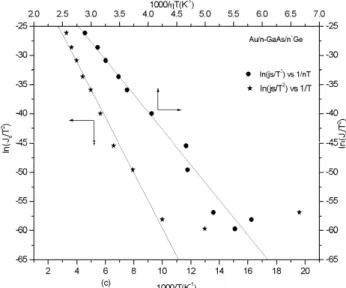
usual and the modified Richardson plots are shown in Fig. 6.
Fig. 6 - The Usual and modified Richardson plots ln(JS/T2) versus 1000/T
CURRENT TRANSPORT BEHAVIOUR OF Au/n-GaAs… 933
energy values (fbo). The non-linearity in ln(JS/T2) versus 1000/T plot at lower temperatures is due to rapid decrease in fbowith fall in temperature.
The values of A** and f
bo obtained from the Richardson plots of the
undertaken Schottky diodes (SD1-SD3) don’t come to any concrete interpretations of the current transport mechanism.
3.3 Effect of barrier inhomogeneity’s
The temperature dependence of Schottky barrier parameters have been reported to be explained on the basis of the barrier height inhomogeneity’s existing in the M-S interface which has been attributed to the variation in thickness, composition of interfaced layer and non-uniformity of interfacial charges. Werner and Guttler [20] explained this abnormal behavior on the basis of Gaussian distribution function with a mean barrier height fbm and
standard deviation sS emanating from the center to the sides and is
represented [19-21],
2
0 S 2
b bm
q KT
s
f =f - çæ ö÷
è ø
(5)
where sS gives the measure of the barrier inhomogeneity.
The plot of fbo versus 1/T using equation (5) is straight line with
intercept at the ordinate determining the mean barrier height (fbm) and
slope the standard deviation (sS). The values of fbm and sS obtained for the
undertaken Schottky diodes have been presented in Table 4. The back substitution of fbm and sS values in equation (5) provides continuous curves
in Fig. 5 for the fbo and h values.
Further, the abnormal behaviour of ideality factors with temperature has been explained by considering the potential fluctuation model [20]. According to this model, the variations in the ideality factors with temperature are given as:
1
1 q S
KT xs g
h = - + (6)
where g and z are the voltage coefficients of barrier heights and standard deviations, respectively.
The plot of 1/h versus 1/T, according to equation (6) should exhibit a straight line with the slope and intercept yielding voltage coefficients of barrier heights, g and standard deviations, z. The values of g and z thus obtained for the undertaken Schottky Diodes are also presented in Table 4. The back substitution of g and z values in equation 6 provided continuous curves for ideality factors in Fig. 5. The existence of ‘Double Gaussian Distribution function’ observed in SD2 and SD3 can also be attributed to some phase transformation occurring at the Schottky Diode interface. The factors responsible for this type of change may be the composition, electrical charges, non-stoichiometry etc. likely to exists at the MS Schottky interface below certain temperature values [22]. Table 4 demonstrates that the mean barrier heights (fbm) increase with epitaxial layer thickness, thus, confirms
934 N. PADHA, R. SACHDEVA, R. SIHOTRA, S.B. KRUPANIDHI
3.4 Thermionic Field Emission
The forward current-voltage characteristics on the basis of thermionic field emission (TFE) can be expressed as [1]:
0
exp( )
S
I =I V E (7)
where
(
)
0 00coth 00
E =E qE KT =hKT q (8)
where E00 is the characteristic energy related to the ‘carrier transmission probability’ through the barrier that determines the relative importance of tunneling [23] represented as:
1 1
2 2
15
* 18.5 10 eV
4
D D
r r e S
N N
h E
m e m
p e
-¥
æ ö æ ö
= ç ÷ = ´ ç ÷
è ø
è ø (9)
Here, me* = (mr, mo), the effective mass of electrons es = (ereo), the
permittivity of the semiconductor and ND, the donor concentration.
According to Padovani and Sumner [23], the characteristic energy, E00 indicates that the current transport mechanism is field emission (FE), if
E00 >> KT; the thermionic- emission (TFE) if E00~KT; and thermionic emission (TE) if E00 << KT.
Further, the ideality factor in case of TFE can be expressed as [23]:
(
)
00 1
E qE KT
h h= = -b (10)
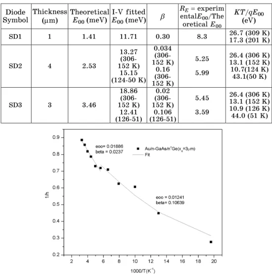
A typical 1/h versus 1000/T plot of the experimental data fitted with theoretically generated curves on the basis of Thermionic Field Emission (TFE) according to equation (10) have been illustrated in Fig. 7. The experimentally observed as well as theoretically generated E00 values for SD1-SD3 are given in Table 5.
Table 4 – Barrier height inhomogeneity parameters of the undertaken
Schottky diodes (SD1-SD3)
Diode
Symbol Thickness fbm (eV) ss g z
SD1 1 0.74 0.07 0.26 0.03
SD2 4 0.93 0.08 0.07 0.05
SD3 3 0.79 (Slope II) 0.86 (Slope I) 0.08 0.07 0.18 0.09 0.09 0.04
It has been observed that in SD1, E00 is 11.71 in the existing temperature range (300-200 K) is anomalously higher than the theoretical
CURRENT TRANSPORT BEHAVIOUR OF Au/n-GaAs… 935
values than theoretical ones as illustrated in Table 5. Further, the condition
KT=E00 is met at low temperatures (below 200 K) in SD1 and SD2. Further, two set of E00 and b values observed at the different temperature regions of Schottky diodes SD2 and SD3 outlines the existence of two distinct phases occurring over the MS interface with a phase transition occurring at 150 K.
Table 5 – The theoretical E00, I-V fitted E00, b and their ratio RE of the undertaken Schottky diodes (SD1-SD3)
Fig. 7 – Plot showing 1/h versus 1000/T along with generated curves using Eq. (10)
giving E00 and b values. The experimental points are also superimposed on the theoretically generated plot shown by solid lines
Therefore, TFE phenomenon is found to exist at low temperatures in the undertaken Schottky diodes and tunneling current component increases with epitaxial layer thickness. Further, it is anomalously high in diodes containing ‘patches’ of reduced barrier heights embedded in the Schottky interface area which demonstrate TFE mechanism even at room temperature.
Diode
Symbol Thickness (mm)
Theoretical
E00 (meV)
I-V fitted
E00 (meV) b
RE= experim entalE00/The
oretical E00
KT/qE00 (eV)
SD1 1 1.41 11.71 0.30 8.3 26.7 (309 K) 17.3 (201 K)
SD2 4 2.53
13.27 (306-152 K)
15.15 (124-50 K)
0.034 (306-152 K)
0.16 (306-152 K)
5.25
5.99
26.4 (306 K) 13.1 (152 K) 10.7(124 K) 43.1(50 K)
SD3 3 3.46
18.86 (306-152 K)
12.41 (126-51)
0.02 (306-152 K)
0.106 (126-51)
5.45
3.59
936 N. PADHA, R. SACHDEVA, R. SIHOTRA, S.B. KRUPANIDHI
This may be ascribed to a mechanism that controls change in electric field or density of states, interface quality, non-stoichiometry etc. at the semi-conductor interface [22, 24].
The changes in the form of increased tunneling current component with change in epitaxial layer thickness observed in the current transport mechanism of the undertaken diodes may be due to the impact of GaAs/Ge hetero-interface over the Au/n-GaAs Schottky barrier.
It is also found that the breakdown voltage decreases with temperature and shows ‘Defect Assisted Tunneling’ phenomenon through surface or defect states in thin epitaxial layer Schottky diodes (~1 mm) while it increases with temperature in thick epitaxial layer Schottky diodes (~3 mm or above) which demonstrate ‘Avalanche Multiplication’ mechanism responsible for junction breakdown. Further, the reverse breakdown voltage is also seen to increase with the epitaxial layer thickness of the diodes.
This finding of tunneling breakdown mechanism is quite different than the conventional breakdown mechanism of Avalanche Multiplication normally observed in Schottky diodes.
Further, the existence of patches significantly change the reverse charac-teristics and the breakdown voltage of the Schottky diodes.
REFERENCES
1. E.H. Rhoderick, R.H. Williams, Metal-semiconductor contacts, 2nd edition
(Oxford: Clarendon: 1988).
2. H.K. Henisch, Semiconductor contacts, (London: Oxford University: 1984). 3. R.T. Tung Mater. Sci. Eng.35, 1 (2001).
4. C.W. Wilmsen, Physics and chemistry of III-V Compound semiconductor interfaces, (New York: Plenum: 1985).
5. A.F. Ozdemir, Semicond. Sci. Technol. 21, 298 (2006).
6. C. Nuhoglu, S. Aydogan, A. Turut, Semicond. Sci. Technol.18, 642 (2003).
7. Y.P. Song, R.L. Van Merihaeghe, W.H. Laflere, F. Cardon, Solid- State Electron.
29,633 (1986).
8. R.T. Tung, A.F. Levi, J.P. Sullivan, F. Schrey, Phys. Rev. Lett. 66, 72 (1991). 9. J.H. Werner, H.H. Gutler, J. Appl. Phys.73, 1315 (1993).
10.C. Detavernier, R. L. Van Meirhaeghe, R. Donaton, K. Maex, F. Cardo J. Appl. Phys. 84, 3226 (1998).
11.S. Forment, R.L. Van Meirhaeghe, A. De Vrieze, K. Strubbe, W.P. Gomes,
Semicond. Sci. Technol. 16, 975 (2001).
12.M.K. Hudait. S.B. Krupanidhi, Physica B307, 125 (2001).
13.F.A. Padovani, R.K. Willardson, A.C. Beer, Semiconductors and Semimetals, Vol. 6 (New York: Academic Press: 1971).
14.S. Ashok, J.M. Borrego, R.J. Gutmann, Solid-State Electron. 22, 621 (1979). 15.Origin ® version 6.0; Microcal software, (Inc. Northampton, MA USA). 16.R.T. Tung, Matter Sci. Eng. 35, 1 (2001).
17.R. Singh, S.K. Arora, R. Tyagi, S.K. Agarwal, D. Kanjilal. Bull. Mater. Sci.
23(6),471 (2000).
18.S.M. Sze, Physics of semiconductor devices, (New York: Wiley: 1981). 19.S. Chand, J. Kumar, Semicond. Sci. Technol.10, 1680 (1995). 20.J.H. Werner, H.H. Gutler. J Appl Phys. 69, 1522 (1991). 21.R.T. Tung, Phys. Rev. B 45(23),13509 (1992).
22.J.Z. Horvath., Solid State Electron. 39, 176 (1996).