258 Brazilian Journal of Physics, vol. 36, no. 2A, June, 2006
Low Frequency Oscillations and Bifurcation Diagram in
Semi-Insulating GaAs Samples
R. L. da Silva1, H. A. Albuquerque1, R. M. Rubinger2, A. G. de Oliveira1, G. M. Ribeiro1, and W. N. Rodrigues1 1Departamento de F´ısica, Instituto de Ciˆencias Exatas, Universidade Federal de Minas Gerais,
Caixa Postal 702, 30123-970, Belo Horizonte, MG, Brazil 2Departamento de F´ısica e Qu´ımica, Instituto de Ciˆencias,
Universidade Federal de Itajub´a, Caixa Postal 50, 37500-903, Itajub´a, MG, Brazil
Received on 4 April, 2005
We present an experimental study of bifurcation diagrams from low frequency current oscillations (LFO) mea-surements obtained from semi-insulating GaAs samples grown by low temperature molecular beam Epitaxy (LT-MBE). The considered growth temperatures were 215 ˚ C and 265 ˚ C. LFO are considered to be spontaneously generated oscillations under constant applied biasV. These oscillations were measurement and recorded in the form of time series. The bifurcation diagrams were obtained from the sequence of minima as a function of the applied bias. The standard measurement procedure was described elsewhere. As the control parameter, the bias allows the identification of a bifurcation route to chaos.
Keywords: Low frequency current oscillations; GaAs; Bifurcation diagrams
I. INTRODUCTION
Semiconductors are appropriate materials for understand-ing nonlinear dynamics phenomena because electrical cur-rents, field, and other quantities can be performed under pre-cisely controlled conditions [1-3]. The semi-insulating (SI) GaAs samples grown by low temperature (LT) molecular beam epitaxy (MBE) present a high density of As anti-site defects (around 1019cm−3). Under extremely varied exper-imental conditions, such as: temperature, infrared illumina-tion, applied bias, etc; these spontaneous currents oscillations under controlled conditions present routes to chaos.
Low frequency oscillations (LFO) are characterized by a frequency range from few Hz to kHz. They occur inside a device and constitute self-organized spatio-temporal struc-tures of electric field domains moving from cathode to an-ode. [1] These oscillations are easy to be observed and mea-sured as nonlinear time series without the need of sophis-ticated instruments. In semiconductors presenting negative differential conductivity (NDC), moving high-field domains can build up spontaneously leading to current oscillations. In semi-insulating GaAs such oscillations occur due to the ef-fect of field enhanced trapping of carriers been captured into deep traps. A route to find the microscopic causes of the LFO is to investigate the carrier generation and recombination processes. In previous works [2,4] using static measurements we presented results that could account for the dominant gen-eration and recombination (g-r) processes. They are, respec-tively, impact ionization and field-enhanced trapping. [2,4] Both processes present characteristics of avalanche and thus are critically dependent on the residual (i.e. obtained at low electric fields or at the ohmic regime) free carrier density.
In a previous work [1], we carried out analysis on ex-perimental LFO, measured in semi-insulating GaAs samples. Those analysis were carried out considering methods of non-linear dynamics analysis of time series and of noise reduction. [5,6]
In the present work, we observe LFO from semi-insulating
GaAs samples, grown to lower temperature than the previous works. [7] The bifurcation diagrams were obtained from the minima sequence of experimental time series as a function of the applied bias. A global view of the underlying dynamics is presented through bifurcation diagrams which are convenient to investigate the periodicity and to classify the bifurcations of the current oscillations versus a control parameter.
II. EXPERIMENTAL DETAILS
The semi-insulating GaAs samples were grown (LT-MBE). Two samples were grown, one at 215oC and the other at 265oC. At these growth temperatures GaAs samples becomes
R. L. da Silva et al. 259
III. EXPERIMENTAL RESULTS
The first sample will be addressed as BH9816 and is the one grown at 215◦C. Fig.1 show the I(V) characteristics for mea-surements at 160K under illumination with a constant current of 15mA through the LED. The curve was traced using an in series circuit consisting of a DC voltage source, the sample and a resistor. For each fixed bias the current was registered as a computer file. The range of the apply biasV was from zero to 100V. Above 20.00V and indicated by the first arrow, is the bias which marks the beginning of oscillatory behavior. For the bias region between both arrows, the sample presents bifurcations.
FIG. 1: I(V) characteristics for BH9816 grown at 215◦C.
We have measured LFO for applied biasV between 20.00 and 30.00V. A typical LFO in chaotic behavior, measured at a temperature of 160K, under illumination with a constant cur-rent of 15mA and fixed DC bias of 25.40V is presented in Fig. 2. These oscillations are evidence of electric field do-mains being destroyed at the anode [9]. The magnitude order of LFO frequencies is of 102Hz.
FIG. 2: Time series for chaotic behavior.
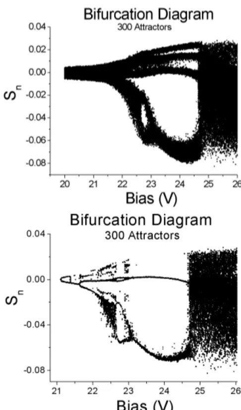
The Fig. 3 shows two bifurcation diagrams obtained from I(t) time series under applied biasV in the domain of 20.00-26.00V with step of 0.02V. Such diagrams were construed by minima sequence{Sn}, of each time series. In Fig. 3b, we
present the bifurcation diagram after the application of the noise reduction algorithm in these time series. As result, the
bifurcation diagram presents a clear region of period-4 cycles. Unfortunately one “arm” of the bifurcation diagram has van-ished with this process.
FIG. 3: Experimental bifurcation diagram of the current minima of the time series as a function of the applied bias in the sample. (a) The original bifurcation diagram, and (b) With noise reduction. Measure-ments were carried at 160K and ILED=15mA.
The second sample grown at 265oC will be addressed as
BH9817. Fig. 4 show the I(V) characteristics measured at 106K under illumination with a constant current of 2mA through the LED. The range of the applied biasV was from zero to 100V. The region between arrows, defines the LFO measurements which we considered for the bifurcation dia-gram. At applied bias within the range of 60.00 to 82.00V we observed high current oscillations, but that were very unstable and hard to register.
260 Brazilian Journal of Physics, vol. 36, no. 2A, June, 2006
In Fig. 5, we have a bifurcation diagram obtained for time series I(t) under applied biasV in the domain of 5.00-10.00V with step of 0.01V. The measurement procedure was the same of the BH9816.
FIG. 5: Experimental bifurcation diagram for the minima of the cur-rent time series as a function of the applied bias. Measurements at 106K with ILED=2mA. Noise reduction for this diagram was not
con-sidered due to signal deformation.
In this bifurcation diagram, we observe a more a new fea-ture. Although hard to identify due to intrinsic noise, the most probable bifurcation sequence is: period-1, period-2, period-4 or period-8 cycles followed by a probable chaos regime. For these data noise reduction algorithm was tested but proved to be inadequate since the signal/noise ratio was very high. As a consequence, the noise reduction algorithm removes part of real signal, resulting in a deformed bifurcation diagram.
IV. SUMMARY
In summary, we measured I(V) and LFO I(t) for LT-MBE GaAs samples at controlled temperature and illumination con-ditions. Bifurcation diagrams were reconstructions from the minima sequence as a function of the applied bias. The noise reduction algorithm applied to the data of both BH9816 and BH9817 samples allowed the cleaning bifurcation, but, in both cases it was harmful to the time series. For the sam-ple BH9817 which presented the worse the signal/noise ratio the noise reduction algorithm have not elucidated the blurred original bifurcation diagram. The bifurcation diagrams pre-sented routes to chaos which resembles the Hopf type diagram with a bifurcation sequence of period-1-2-4 cycles and possi-ble period-8 cycles followed by a possipossi-ble chaos. Finally, the reduction of periodicity in the bifurcation sequence of both samples might be an evidence of a complex dependence on the control parameter: temperature, illumination and applied DC biasV, of the experimental system. And the competition on g-r processes. We will discuss this in detail in another work which considers time series obtained from numerical integra-tion of a differential equaintegra-tion system of a physical model of the relevant g-r mechanisms considered for the present work.
Acknowledgements
The authors would like to acknowledge the Brazilian agen-cies CNPq and FAPEMIG for financial support.
[1] R. M. Rubinger, R. L. da Silva, A. G. de Oliveira, G. M. Ribeiro, and H. A. Albuquerque, Chaos13, 457 (2003).
[2] R. M. Rubinger, A. G. de Oliveira, J. C. Bezerra, G. M. Ribeiro, W. N. Rodrigues, and M. V. B. Moreira, Phys. Rev. B62, 1859 (2000).
[3] G. N. Maracas, W. Porod, D. A. Johnson and K. Ferry, Physica B134, 276 (1985).
[4] H. A. Albuquerque, A. G. de Oliveira, G. M. Ribeiro, R. L. da Silva, W. N. Rodrigues, M. V.B. Moreira, and R. M. Rubinger, J.
Appl. Phys.93, 1647 (2003).
[5] H. D. I. Abarbanel, R. Brown, J. J. Sidorowich, and L. Sh. Tsim-ring, Rev. Mod. Phys.65, 1331 (1993).
[6] R. Hegger, H. Kantz and T. Schreiber, Chaos9, 413 (1999). [7] R. L. da Silva, H. A. Albuquerque, R. M. Rubinger, A. G. de
Oliveira, and G. M. Ribeiro, Physica D194, 166 (2004). [8] T. Schreiber, Phys. Rev. E47, 2401 (1993).