GAMMA-RAY IR RA DI A TION AND POST-IR RA DI A TION AT
ROOM AND EL E VATED TEM PER A TURE RE SPONSE OF
pMOS DO SIM E TERS WITH THICK GATE OX IDES
by
Mom~ilo M. PEJOVI] 1*, Svetlana M. PEJOVI] 2,
Edin ]. DOLI]ANIN 3, and Djordje LAZAREVI] 4
1
Fac ulty of Elec tronic En gi neer ing, Uni ver sity of Niš, Niš, Ser bia 2
State Uni ver sity of Novi Pazar, Novi Pazar, Ser bia 3
Fac ulty of Elec tri cal En gi neer ing, Uni ver sity of Bel grade, Bel grade, Ser bia 4 Vin~a In sti tute of Nu clear Sci ences, Uni ver sity of Bel grade, Ser bia
Sci en tific pa per UDC: 621.386.82:621.382.3 DOI: 10.2298/NTRP1103261P
Gamma-ray ir ra di a tion and post-ir ra di a tion re sponse at room and el e vated tem per a ture have been stud ied for ra di a tion sensitive pMOS tran sis tors with gate ox ide thick ness of 100 and 400 nm, re spec tively. Their re sponse was fol lowed based on the changes in the thresh old volt -age shift which was es ti mated on the ba sis of trans fer char ac ter is tics in sat u ra tion. The presence of ra di a tion-in duced fixed oxide traps and switch ing traps – which lead to a change in the thresh old volt age – was es ti mated from the sub-thresh old I-V curves, us ing the midgap tech nique. It was shown that fixed ox ide traps have a dom i nant in flu ence on the change in the thresh old volt age shift dur ing gamma-ray ir ra di a tion and an nealing.
Key words: pMOS do sim e ter, gamma-ray ir ra di a tion, thresh old volt age shift, ab sorbed dose
IN TRO DUC TION
It is well known that ion iz ing ra di a tion causes the deg ra da tionof elec tronic com po nents and ma te ri -als [1]. It is -also known that gamma-ra di a tion leads to the cre ation of de fects re spon si ble for the in crease in the pos i tive charge of the gate ox ide and in ter face states on the Si/SiO2 in ter face of MOS com po nents and in te grated cir cuits [2-4]. Ra di a tion de fects lead to the in sta bil ity of MOS tran sis tors by chang ing their elec tric pa ram e ters [1]. Rec og niz ing these defects is im por tant if MOS com po nents resistant to this type of ra di a tion are to be re al ized.
Orig i nat ing in the 1970s[5], the idea of us ing a pMOS tran sis tor with an Al-gate as a do sim e ter of gammaray ir ra di a tion (also known as the pMOS do sim e ter or RADFET) based on the in crease of tran sis tor sen si tiv ity to ir ra di a tion, has since been fur ther de -vel oped [6-9]. Pos si ble prac ti cal ap pli ca tions of pMOS dosimeters are, in deed, wide: their use as per -sonal do sim e ters, in the lab o ra tory, ra di a tion ther apy, space craft, nu clear equip ment, and so on [10]. The pMOS do sim e ter, apart from the ex pres sive thresh old volt age shift dur ing ir ra di a tion, has to satisfy an other cri te rion upon ir ra di a tion: long-term sta bil ity of the
thresh old volt age shift at room tem per a ture (fad ing), i. e., the ne ces sity of sav ing the in for ma tion on the ra -di a tion dose ab sorbed.
The ba sic con cept of a pMOS dosimeter is to con vert the thresh old volt age shift, DVT, in duced by ra di a tion, into the ab sorbed ra di a tion dose, D. This de -pend ence can be ex pressed in the form of [11, 12]
DVT = ADn
(1)
where DVT = VT – VT0, VT0 is the thresh old volt age af ter
ir ra di a tion, VT0 – the onebe fore ra di a tion, A – the con
-stant and n – the de gree of lin ear ity. Ide ally, this de -pend ence is lin ear, i. e., n = 1, where A rep re sents the sen si tiv ity, S of the pMOS do sim e ter
S V
D
=
D T
(2)
also been shown that the sen si tiv ity of a pMOS do sim -e t-er is -en -ergy-d-e p-end -ent [16, 17], -ex pr-ess-ed by th-e dose en hance ment fac tor which rep re sents the ra di a tion be tween the sen si tiv ity at in ci dent ra di a tion en -ergy and the sen si tiv ity of pho tons from the source
27 60Co.
EX PER I MEN TAL DE TAILS
The ex per i mental sam ples used in this study were Al-gate pMOS tran sis tors man u fac tured by the Tyn dall Na tional In sti tute, Cork, Ire land [18]. Gate ox ides of 100 and 400 nm, re spec tively, were grown at 1000 °C in dray ox y gen and an nealed for 15 minutes at 1000 °C in ni tro gen. The post-metallization an neal was per formed at 440 °C in form ing gas for 60 minutes.
Irradiation was per formed in the Me trol ogy Lab -o ra t-ory -of the Vin~a In sti tute of Nu clear Sci ences, Bel -grade. The pMOS do sim e ters were irradiated at room tem per a ture us ing a source to the ab sorbed dose of D = 35 Gy (Si), at the ab sorbed dose rate D = 0.02 Gy (Si) s–1. The gate bias dur ing ir ra di a tion was V
irr = 5 V (the other pins were grounded). Immediately af ter ir ra di a tion, pMOS do sim e ters were an nealed at room tem perature for a time pe riod of 5232 hours with out po lar -iza tion (all pins were grounded). Af ter that, an neal ing on a tem per a ture of 120 °C, also with out po lar iza tion on the gate and last ing 423 hours, was con tin ued. The pMOS do sim e ter thresh old volt age be fore ir ra di a tion, VT0, as well as dur ing ir ra di a tion and an neal ing, VT, were de ter mined by trans fer char ac ter is tics in sat u ra -tion, i. e., the in ter sec tion be tween the VGaxis and ex -trap o lated lin ear re gion of the (ID)1/2- V
G [19], where
VG is the gate volt age and ID is the drain cur rent. The IV char ac ter iza tion was per formed by a Keithley 4200 SCS (Semi con duc tor Char ac ter iza tion Sys tem) unit. The sys tem is equipped with three me -dium power source-mea sur ing units (4200 SMU) for IV char ac ter iza tion. The source-mea sur ing units have four volt age ranges: 200 mV, 2 V, 20 V, and 200 V, while the cur rent ranges are 100 mA, 1 mA, 100 mA, and 1 mA. One of the source-mea sur ing units is equipped with a preamplifier which pro vides the mea -sure ment of very low cur rents (in the or der of pA).
Aerial den si ties of ra di a tion-in duced fixed traps, DNft, and switch ing traps, DNst, dur ing ir ra di a tion and an neal ing were de ter mined from the sub-thresh old I-V curves, us ing the midgap tech nique (MGT) of
McWhoter and Winocur [20]. Fixed traps (FT) rep re -sent traps cre ated in the ox ide, while switch ing traps (ST) rep re sent traps cre ated near and at the Si/SiO2 in -ter face. The ST cre ated in the ox ide, near the SiO2/Si in ter face, are called slow switch ing traps (SST), ST cre ated at the in ter face, fast switch ing traps (FST) or true in ter face traps. FT rep re sent traps in the ox ide that do not cap ture the car ri ers from the chan nel, but SST and FST, mak ing the ST, rep re sent traps that do cap -ture (com mu ni cate with) the car ri ers from the chan nel within the time frames of elec tri cal MGT mea sure -ments.
The con tri bu tion of FT (DVft) and ST (DVst) to the net thresh old volt age shift DVT is [11]
DVT = DVft + DVst (3)
while the den si ties of DNft and DNst af ter irra di a tion
and an neal ing may be de ter mined as [20]
DN C DV D D
q N
C V q
ft = ox ft ; st = ox st (4)
where Cox is the ox ide ca pac i tance per unit area and q
the ab so lute value of the elec tron charge.
RE SULTS AND DIS CUS SION
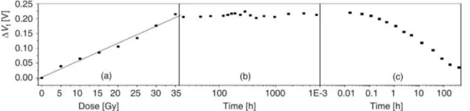
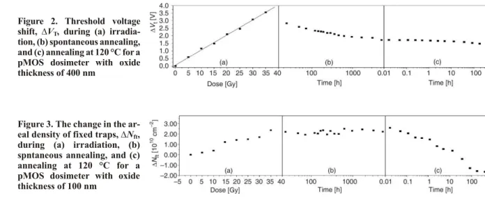
Fig ures 1(a) and 2(a) rep re sent the DVT = f(D) de pend ence dur ing irradiation of pMOS do sim e ters with a gate ox ide tick of 100 nm and 400 nm, re spec -tively. It is ob vi ous that the changes in the thresh old volt age shift dur ing ir ra di a tion are sig nif i cantly higher in do sim e ters with larger ox ide thick ness, a re sult to be ex pected.
Sym bols in the fig ures shown rep re sent the DVT = VT – VT0 val ues ob tained from pMOS do sim e -ters trans fer char ac ter is tics in sat u ra tion, while the solid lines are de ter mined by the fit ting of this data with the ex pres sion (1) for the de gree of lin ear ity n = 1. The val ues of fit ting cor re la tion fac tors for pMOS do -sim e ters with gate ox ide thick ness of 100 nm and 400 nm were 0.99291 and 0.99852, re spec tively. Be -cause the cor re la tion fac tors are very close to one, it can be as sumed that there is a lin ear de pend ency be -tween DVT and D, i. e., that the sen si tiv ity of these do -sim e ters can be de ter mined on the ba sis of ex pres sion (2).
Fig ures 1(b) and 2(b) show the DVT evo lu tion of ir ra di a tion pMOS do sim e ters with a gate ox ide tick of
Fig ure 1. Thresh old volt age shift, DVT, dur ing (a) ir ra di a tion, (b)
100 nm and 400 nm, re spec tively, dur ing an neal ing at room tem per a ture (also known as spon ta ne ous re cov -ery of fad ing). In pMOS do sim e ters with gate ox ide thick ness of 100 nm, the value DVT changes in sig nif i -cantly dur ing spon ta ne ous re cov ery, i. e., in these tran -sis tors the dosimetric in for ma tion is saved. In pMOS do sim e ters with gate ox ide thick ness of 400 nm, fig. 2(b), the value of DVT de creases dur ing spon ta ne ous re cov ery in the first 1000 hours and af ter wards DVT re -mains an ap prox i mately con stant value. There fore, in these tran sis tors there is a loss of the dosimetric in for -ma tion at the be gin ning of spon ta ne ous re cov ery.
For the pur pose of check ing whether the pro cess of the loss of dosimetric in for ma tion af ter spon ta ne ous an neal ing oc curred, the an neal ing of pMOS do sim e -ters at a tem per a ture of 120 °C was con tin ued and the re sults of this kind of an neal ing shown in figs, 1(c) and 2(c). It can be seen that in pMOS do sim e ters with gate ox ide thick ness of 100 nm, fig. 1(c), there is a rapid loss of value of DVT dur ing an neal ing. It shows that, for the times of an neal ing lower than 423 hours, in these do sim e ters there is a com plete loss of dosimetric in for ma tion. In pMOS do sim e ters with gate ox ide thick ness of 400 nm, fig. 2(c), fur ther loss of dosimetric in for ma tion is slight.
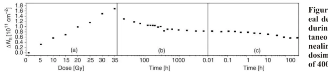
Fig ures 3(a) and 4(a) show the be hav ior of DNft dur ing ir ra di a tion for pMOS do sim e ters with gate ox -ide thick ness of 100 nm and 400 nm, respectively. It could be seen that the value DNft for pMOS do sim e ters with larger ox ide thick ness is ap prox i mately an or der of mag ni tude higher than in pMOS do sim e ters with smaller ox ide thick ness. Dur ing spon ta ne ous an neal -ing in pMOS do sim e ters with gate ox ide thick ness of 100 nm, fig. 3(b), there is an in sig nif i cant change in DNft value. In pMOS do sim e ters with gate ox ide thick ness of 400 nm, at the be gin ning of spon ta ne ous re cov -ery, there is a sig nif i cant de crease of DNft value, fig. 4(b), af ter which this change is in sig nif i cant.
Fig ures 3(c) and 4(c) show the be hav ior of DNft dur ing con tin u ous an neal ing at an el e vated tem per a
-ture. As could be seen, el e vated tem per a ture in pMOS do sim e ters with gate ox ide thick ness of 100 nm leads to a rapid de crease in DNft value dur ing an neal ing to 100 hours. In pMOS do sim e ters with gate ox ide thick -ness of 400 nm, fig. 4(c), DNft value in sig nif i cantly changes dur ing an neal ing.
Dur ing ir ra di a tion and later an neal ing at room and el e vated tem per a ture, be sides the change in DNft, a change of DNst oc curs. How ever, the change of DNft in both types of pMOS do sim e ters is an or der of mag ni -tude higher than the change of DNst (re sults for DNst are not shown in this pa per). This shows that the dom i nant in flu ence on DVT, i. e., on the dosimetric in for ma tion, lies in FT which are formed in the gate ox ide dur ing gamma-ray ir ra di a tion. For this rea sons, the role of FT in the for ma tion and sav ing of dosimetric in for ma tion will be dis cussed in this pa per.
Ex per i men tal re sults shown in figs. 3 and 4 can be most readily ex plained within the model given in pa pers [21-23]. The crit i cal role in this model be longs to the Eg cen ter, a weak Si-Si bond in the ox ide caused by an ox y gen atom va cancy be tween two Si at oms, each back-bounded to three ox y gen at oms [24]. The Eg cen ter acts as a hole trap and is pre dom i nately re spon si ble for the in crease in the ox ide trapped charge dur ing ir ra di a tion [25]. We will ac cept the con vinc ing ar -gu ments of Lelis and Oldham [23] that the switch ing ox ide traps in ir ra di ated ox ides are Eg cen ters close to the Si/SiO2 in ter face. The fixed ox ide traps are, mi cro -scop i cally, Eg cen ters as well – how ever, fur ther from the Si/SiO2 in ter face and hence in ca pa ble of ex chang ing charge with Si dur ing the time frame of the mea -sure ments.
The ox ide trapped charge in volves both the charge trapped at fixed ox ide traps and that trapped at switch ing ox ide traps. Namely, un der the in flu ence of the pos i tive elec tric field in the ox ide (caused by pos i -tive gate bias) dur ing an neal ing, the hole trapped at the Eg cen ter can be ei ther com pen sated or neu tral ized by the elec tron tun nel ing from Si.
Fig ure 2. Thresh old volt age shift, DVT, dur ing (a) ir ra di a
-tion, (b) spon ta ne ous an neal ing, and (c) an neal ing at 120 °C for a pMOS do sim e ter with ox ide thick ness of 400 nm
Fig ure 3. The change in the ar -eal den sity of fixed traps, DNft,
Based on the be hav ior of DNft dur ing spon ta ne -ous an neal ing of pMOS do sim e ters with gate ox ide thick ness of 100 nm, fig. 3(b), it can be con cluded that the tun nel ing of elec trons from Si does not have a sig -nif i cant ef fect on the com pen sa tion or neu tral iza tion of Eg cen ters. In pMOS do sim e ters with gate ox ide thick ness of 400 nm, fig. 4(b), in the first 1000 hours, the tun nel ing of elec trons from Si leads to a par tial com pen sa tion or neu tral iza tion of Eg cen ters dur ing an neal ing.
When exposing pMOS tran sis tors to el e vated tem per a tures af ter spon ta ne ous an neal ing, an added mech a nism ap pears which leads to the com pen sa tion or neu tral iza tion of FT. Namely, be sides the neu tral -iza tion or com pen sa tion of the charge trapped at Eg centers by elec trons tun nel ing from Si un der the in flu -ence of the elec tri cal field, elec trons ther mally emit ted from the ox ide va lence band also con trib ute to the neu -tral iza tion of the Eg cen ter [26].
As can be seen in figs. 3(c) and 4(c), de crease in the value of DNft dur ing an neal ing at an el e vated tem -per a ture is much faster in pMOS do sim e ters with gate ox ide thick ness of 100 nm. This shows that in these do sim e ters the neu tral iza tion of Eg is due to the elec -trons ther mally emit ted from the ox ide va lence band much more ef fi ciently than in pMOS do sim e ters with a gate ox ide thick ness of 400 nm. Namely, el e vated tem per a tures in pMOS do sim e ters with gate ox ide thick ness of 100 nm, fig. 3(c), lead to com plete neu -tral iza tion ofEg cen ters which were formed dur ing ir -ra di a tion, along with parts of Eg cen ters formed dur ing technological pro cesses used in the man u fac tur ing of these components. In pMOS do sim e ters with a gate ox ide thick ness of 400 nm, the loss of re main ing dosimetric in for ma tion slightly de creased af ter 423 hours of an neal ing, which goes to say that the elec -trons ther mally emit ted from the ox ide va lence bond do not have a sig nif i cant in flu ence on the neu tral iza -tion of Eg cen ters.
CON CLU SIONS
On the ba sis of what was stated above, the fol -low ing con clu sion may be reached. Dur ing gamma-ray ir ra di a tion to the dose of 35 Gy, there is an ap prox i mately lin ear de pend ency be tween the thresh -old volt age shift and the ab sorbed dose in both types of
pMOS do sim e ters, mak ing these com po nents use ful as sen sors of high dose range gamma-ray ir ra di a tion. How ever, pMOS do sim e ters with gate ox ide thick ness of 400 nm are more suit able as sen sors be cause they ex hibit higher thresh old volt age changes dur ing ir ra di a tion. Dur ing spon ta ne ous an neal ing in pMOS do -sim e ters with a gate ox ide thick ness of 100 nm, the thresh old volt age shift re tains an ap prox i mately con -stant value, i. e., at room tem per a ture dosimetric in for ma tion is kept for a pe riod of 218 days. In pMOS do -sim e ters with gate ox ide thick ness of 400 nm, dur ing spon ta ne ous an neal ing of 50 days, the thresh old volt -age shift de creases, i. e., a par tial loss of dosimetric in -for ma tion oc curs. The continuation of an neal ing at a tem per a ture of 120 °C leads to a complete loss of dosimetric in for ma tion in pMOS do sim e ters with a gate ox ide thick ness of 100 nm – which is not the case with pMOS tran sis tors with a gate ox ide thick ness of 400 nm. Eg cen ters play a crit i cal role in the pMOS do -sim e ter re sponse, be ing re spon si ble for both fixed and switching traps in the ox ide and hole and elec tron trap ping. There fore, the need to op ti mize the pMOS do -sim e ter fab ri ca tion pro cess in terms of Eg cen ter num -bers, lo ca tion and en ergy, is of par a mount importance. This can be done by op ti miz ing the highest tem per a -ture pro cess, usu ally gate ox i da tion and sub se quent an neal, in an in ert at mo sphere. However, one should be care ful when com ing to conclusions, be cause some times the whole pro cess se quence rather than in -di vid ual pro cess steps can im pact the ra -di a tion and post-ir ra di a tion re sponse of the de vices.
AC KNOWL EDGE MENTS
This work was sup ported by the Min is try of Sci -ence and Tech no log i cal De vel op ment of the Re pub lic of Ser bia un der con tract 171007.
REF ER ENCES
[1] Ma, T. P., Dressendorfer, P. V., Ion iz ing Ra di a tion Ef -fects in MOS De vices and Cir cuits, John Wihley and Sons, New York, USA, 1989
[2] Pejovi}, M., Risti}, G., Cre ation and Possivation of In ter face Traps in Ir ra di ated MOS Tran sis tors dur ing An neal ing at Dif fer ent Tem per a tures, Solid-State Elec tron ics, 41 (1997), 5, pp. 715-720
Fig ure 4. The change in the ar -eal den sity of fixed traps, DNft,
[3] Pejovi}, M., Risti}, G., Jakši}, A., For ma tion and Passivation of In ter face Traps in Ir ra di ated n-Chan nel Power VDMOSFETs dur ing Ther mal An neal ing, Ap -plied Sur face Sci ence, 108 (1997), 1, pp. 141-148 [4] Vuki}, V., Osmokrovi}, P. V., Im pact of For ward
Emit ter Cur rent Gain and Ge om e try of PNP Power Tran sis tors on Ra di a tion Tol er ance of Volt age Reg u -la tors, Nu clear Tech nol ogy & Ra di a tion Pro tec tion, 25 (2010) 3, pp. 179-185
[5] Holmes-Siedle, A., The Space Charge Do sim e ter, Nucl. Instrum. Meth ods, 121 (1974), 1, pp. 169-179 [6] Holmes-Siedle, A., Ad ams, L., RADFET: A Re view
of the Use of MetalOx ideSil i con De vices as In te -grat ing Do sim e ters, Ra dial. Phys. Chem., 28 (1986), 2, pp. 235-244
[7] Hughes, R. C., et al., Dual Di elec tric Sil i con Metal-Ox ide-Semi con duc tor Field-Ef fect Tran sis tors as Ra di a tion Sen sors, J. Appl. Phys., 65 (1989), 5, pp. 1972-1976
[8] Kelleher, A., et al., De vel op ment of Ra di a tion Sen si -tive of pMOS Do sim e ters, IEEE Trans. Nucl. Sci., NS-39 (1992), 3, pp. 342-346
[9] Risti}, G., Golubovi}, S., Pejovi}, M., Sen si tiv ity and Fad ing of pMOS Do sim e ters with Thick Gate Ox ide, Sen sors Ac tu a tors A: Phys. A 51 (1996), 2-3, pp. 153-158
[10] Risti}, G. S., In flu ence of Ion iz ing Ra di a tion and Hot Car rier In jec tion on MetalOx ideSemi con duc tor Tran -sis tors, J. Phys. D: Appl. Phys., 41 (2008), 023001, p. 19 [11] Risti}, G. S., Ther mal and UV An neal ing of Ir ra di ated
pMOS Dosimetric Tran sis tors, J. Phys., D: Appl. Phys., 42 (2009), 135101, p. 12
[12] Risti}, G., Golubovi}, S., Pejovi}, M., pMOS Tran sis -tors for Dosimetric Ap pli ca tion, Electr. Lett., 29 (1993), 18, pp. 1644-1645
[13] Ensell, G., HolmesSiedle, A., Ad ams, L., Thick Ox ide pMOSFET Do sim e ters for High En ergy Ra di a -tion, Nucl. Instr. Meth ods Phys. Res. A 269 (1988), 3, pp. 655-658
[14] Kelleher, A., Lane, W., Ad ams, L., A De sign So lu tion to Intereasing the Sen si tiv ity of pMOS Do sim e ters: the Stacked RADFET Ap proach, IEEE Trans. Nucl. Sci. NS-42 (1995), 1, pp. 48-51
[15] O’Connel, B., et al., Sacked RADFETs for In creased Ra di a tion Sen si tiv ity, IEEE Trans. Nucl. Sci., NS-43 (1996), 3, pp. 985-990
[16] Brucker, G. J., Kronenberg, S., Gentner, F., Ef fects on Pack age Ge om e try, Ma te ri als, and Die De sign of En -ergy De pend ence of pMOS Do sim e ters, IEEE Trans. Nucl. Sci., NS-42 (1995), 6, pp. 33-40
[17] Spinc, Z., et al., En ergy De pend ence of pMOS Do sim -e t-ers, Radiat. Prot. Dosim., 64 (1996), 2, pp. 205-211 [18] Pejovi}, M. M., Pejovi}, M. M., Jakši}, A. B., Ra di a -tion-Sen si tive Field Ef fect Tran sis tors Responce to Gamma-Ray Ir ra di a tion, Nu clear Tehnology & Ra di -a tion Pro tec tion, 26 (2011), 1, pp. 25-31
[19] Sze, S. M., Phys ics of Semi con duc tor De vices, John Wiley and Sons, New York, USA, 1981
[20] McWharter, P. J., Winokur, P. S., Sim ple Tech nique for Sep a rat ing the Ef fects of In ter face Traps and TrappedOx ide Charge in MetalOx ide Semi con duc -tor Tran sis -tors, Appl. Phys. Lett., 48 (1986), 2, pp. 133-135
[21] Lelis, A. J., et al., Re vers ibil ity of Trapped Hole An -neal ing, IEEE Trans. Nucl. Sci., 35 (1988), 6, pp. 1186-1191
[22] Lelis, A. J., et al., The Na ture of the Trapped Hole An -neal ing Pro cess, IEEE Trans. Nucl. Sci., 36 (1989), 6, pp. 1808-1815
[23] Lelis, A. J., Oldham, T. R., Time De pend ence of Switch ing Ox ide Traps, IEEE Trans. Nucl. Sci., 41 (1994), 6, pp. 1835-1843
[24] Feigl, F. J., Fowler, W. B., Yip, K. L., Ox y gen Va -cancy Model for the Cen ter in SiO2, Solid-State Commun., 14 (1974), 3, pp. 225-229
[25] Lenahan, P. M., Dressendorfer, P. V., Hole Traps and Tri va lent Sil i con Cen ters in Metal /Ox ide/ Sil i con De -vices, J. Appl. Phys., 55 (1984), 10, pp. 3495-3499 [26] McWharter, P. J., Miller, S. L., Miller, W. M., Mod el
-ing the An neal of Ra di a tion-In duced Trapped Holes in a Vary ing Ther mal En vi ron ment, IEEE Trans. Nucl. Sci., 37 (1990), 6, pp. 1682-1689
Re ceived on July 15, 2011 Ac cepted on Oc to ber 21, 2011
Mom~ilo M. PEJOVI], Svetlana M. PEJOVI], Edin ]. DOLI]ANIN, \or|e LAZAREVI]
ODZIV pMOS DOZIMETARA SA DEBELIM OKSIDIMA UPRAVQA^KE ELEKTRODE, TOKOM GAMA ZRA^EWA I POSLE OZRA^IVAWA
NA SOBNOJ I POVI[ENOJ TEMPERATURI
Istra`ivan je odziv radijaciono osetqivih pMOS tranzistora ~ije su debqine oksida
100 nm i 400 nm tokom gama zra~ewa i kasnijeg oporavka na sobnoj i povi{enoj temperaturi. Odziv
ovih tranzistora je pra}en na osnovu promene napona koji je procewivan iz prenosnih karakteristika u saturaciji. Prisustvo centara u oksidu upravqa~ke elektrode kao i centara na me|upovr{ini silicijum-silicijumdioksid, koji dovode do promene napona praga, procewivani su tehnikom koja koristi pretpragovske strujno-naponske krive. Pokazano je da dominantnu ulogu u promeni napona praga tokom ozra~ivawa i kasnije oporavka imaju centri zahvata u oksidu gejta.