IM PROVE MENT POS SI BIL I TIES OF THE I-V
CHAR AC TER IS TICS OF PIN PHOTODIODES DAM AGED
BY GAMMA IR RA DI A TION
by
Dejan S. NIKOLI] 1, Aleksandra I. VASI] 2,
Djordje R. LAZAREVI] 3*, and Marija D. OBRENOVI] 2
1
Br~ko Dis trict Gov ern ment, Br~ko, Bosnia and Herzegovina 2
Fac ulty of Me chan i cal En gi neer ing, Uni ver sity of Bel grade, Bel grade, Ser bia 3
Ra di a tion Pro tec tion Lab o ra tory, Vin~a In sti tute of Nu clear Sci ences, Bel grade, Ser bia
Sci en tific pa per DOI: 10.2298/NTRP1301084N
This pa per pres ents the be hav ior of PIN photodiodes af ter com bined gamma and neu tron ir -ra di a tion. Dif fer ent types of PIN photodiodes have been ex posed first to gamma and then to neu tron ir ra di a tion. I-V char ac ter is tics (cur rent de pend ence on volt age) of photodiodes have been mea sured af ter each of these ir ra di a tions. It has been noted that the photocurrent level af ter the neu tron ir ra di a tion is higher than be fore it, which is not con sis tent with the cur rent the o ries about the ef fects of neu tron ra di a tion on semi con duc tors. In or der to ex plain this be hav ior of the photodiodes, the Monte Carlo sim u la tion of pho ton trans port through the ma -te rial has been used. It is pro posed that a pos si ble cause for cur rent en hance ment are de fects in semi con duc tor cre ated by gamma ir ra di a tion and ef fects of neu tron ir ra di a tion on these de -fects. The re sults can be ex plained by an intercentre trans fer of charge be tween de fects in close prox im ity to each other. The aim of this pa per is to in ves ti gate the im prove ment pos si bil i ties of the I-V char ac ter is tics of PIN photodiodes, and photodetectors in gen eral, dam aged by gamma ir ra di a tion.
Key words: PIN photodiode, gamma ir ra di a tion, neu tron ir ra di a tion, I-V char ac ter is tic, Monte Carlo sim u la tion
INTRODUCTION
Mod ern mea sure ments are mainly based on the con ver sion of phys i cal quan ti ties to elec tri cal sig nals. The ba sic measuring de vices which en able the re ceiv -ing of in for ma tion in the au to matic con trol sys tem are sen sors.
The main rea son why op to el ec tronic sen sors at -tract the at ten tion of many re search ers and us ers is the phe nom e non of change of the op ti cal sig nal pa ram e -ters by chang ing of mea sured phys i cal quan tity as the ba sic func tion ing prin ci ple of op to el ec tronic sen sors. In func tional terms, op ti cal sen sors are more flex i ble, more re li able and more uni ver sal than con ven tional sen sors, be cause of the pos si bil ity of use in all con di -tions with strong mag netic fields, elec tri cal noise, chem i cal cor ro sion, etc.
On the other hand, now a days, due to the high tech no log i cal de vel op ment, one is un der the con stant in flu ence of the en tire spec trum of elec tro mag netic ra
di a tion, which co mes from nat u ral sources and the de vices that man has cre ated him self. The trend of min ia tur iza tion and the higher de gree of elec tronic com po -nents in te gra tion has re sulted in in creased sen si tiv ity of these com po nents to the ef fects of ion iz ing ra di a tion. The tech no log i cal pro cess of large scale in te gra -tion cir cuits of ten in cludes bom bard ment with highen ergy ions or pho tons, which can lead to sig nif i -cant ra di a tion dam age.
In re cent pa pers the be hav ior of var i ous op to el ec tronic de vices in terms of gamma and neu tron ra di a -tion has been ob served [1-6]. Photodiodes, as one of the most used and the sim plest types of op ti cal sen sors, have been an a lyzed in most pa pers. The in flu ence of gamma and neu tron ir ra di a tion on semi con duc tors in gen eral (and es pe cially on the photodiodes) is very well known and de scribed in sev eral pa pers and text -books.
time to re cover. Though the ef fect of gamma ra di a tion fol lows the well-known the o ret i cal model (which is man i fested in the re duc tion of photocurrent), the sub -se quent neu tron ir ra di a tion on the photodiodes cau-ses the op po site ef fect from the the o ret i cal model, so the photocurrent in creases.
The aim of this pa per is to ex plain the pro cesses that oc cur in the photodiode af ter gamma and neu tron ra di a tion and to try to find the way of im prov ing the char ac ter is tics of photodiodes, and photodetectors in gen eral, dam aged by gamma ir ra di a tion.
THEORETICAL ANALYSIS
There are sev eral in ter ac tion mech a nisms of elec tro mag netic ra di a tion with the ma te rial (the elas tic in co her ent Thomson scat ter ing, the elas tic co her ent Ray leigh scat ter ing, the in elas tic Compton scat ter ing, the pho to elec tric ef fect, the nu clear photoeffect, the pro duc tion of elec tron-pos i tron pairs).
Gamma ray (high en ergy pho tons) in ter acts with or bital elec trons via pho to elec tric and Compton ef -fects. If the en ergy of gamma ray is high enough (above sev eral hun dred keV) the pair gen er a tion oc -curs. The en ergy spec trum of the en er getic elec trons is called “slow ing spec trum”. The en er getic elec tron in -ter acts with a lat tice atom. As a re sult, the lat tice atom is dis placed from the lat tice site. This is so called pri -mary knock on atom (PKA) [7, 8]. In ter sti tial PKA, va cancy, and com plex of them form a deep level in bandgap (socalled the gen er a tionre com bi na tion cen -tre). The re com bi na tion cen ters in bulk re gion cause the re duc tion of car rier life time. In ad di tion the deep lev els com pen sate the do nor or ac cep tor lev els re sult -ing in the re duc tion of ef fec tive car rier con cen tra tion car rier re moval (CR) ef fect. It af fects the de ple tion layer width by be com ing wider.
On the other hand, as rel a tively heavy and un -charged par ti cles, neu trons col lid ing with at oms in the crys tal lat tice cause dis place ment of at oms from the lat tice. A pair of in ter sti tial atom and va cancy are called the Frencel de fect. If the in ci dent neu tron en -ergy is high enough, it can de liver enough en -ergy to the dis placed atom which can dis place other at oms in the lat tice. This re quires fast neu trons with en er gies from 10 keV to 10 MeV. Shift ing va can cies con nect with the im pu rity at oms, do nors and other va can cies form ing tem per a ture sta ble de fects (com plex de fects) which rep re sent re com bi na tion cen ters and trap cen ters, sig nif i cantly re duc ing the mi nor ity car rier life -time [8, 9].
The fi nal re sult of both gamma and neu tron ra di -a tion on photodiodes is in cre-as ing of re com bi n-a tion cen ters con cen tra tion, which, ac cord ing to the ShockleyRead for mula [9], di rectly re sulted in de -creas ing the mi nor ity car rier life time
t d d d d = á ñ + +
+ + +á ñ
+ +
+ +
1 1 1 1
c N
n n n
n p n c N
n p p n p p
n t
o
o o n t
o
o o
(1)
where t = tp = tn is the life time of elec trons and holes
and Nt con cen tra tion of Rcen tres (re com bi na tion cen -tres which can ac cept both elec trons and holes).
The re duc tion of mi nor ity car rier life time causes photocurrent de creas ing.
Pre vi ously stated ex pla na tion is re lated to the in -flu ence of neu tron ir ra di a tion on the new, pre vi ously non-ir ra di ated photodiodes. How ever, if we change the ini tial con di tions i. e. if the photodiode pre vi ously has been ex posed to some elec tro mag netic ra di a tion such as gamma ra di a tion, the ef fects of neu tron ir ra di a tion will be dif fer ent. In that case the dam age struc -ture from neu tron ir ra di a tion leads to clus ters of intrinstic de fects such as divacancies.
The divacancy has three en ergy lev els in the bandgap: a hole trap and two ac cep tor states. In stan -dard Shockley-Read-Hall the ory, cur rent gen er a tion in sil i con de ple tion re gions is me di ated by iso lated de fect lev els in the for bid den bandgap. Gen er a tions oc -curs when a hole is emit ted from the de fect level into the va lence band (i. e. elec tron cap tured from it) and an elec tron is emit ted into the con duc tion band. Each tran si tion oc curs with a rate, en or ep, and is gov erned by the time con stant t
ne or tpe. If sev eral de fect lev els
ex ist, they are re garded as the sum of the in di vid ual com po nents. In cou pled de fect gen er a tion, il lus trated in fig. 1, an elec tron is first cap tured by the do nor state in the bot tom half of the bandgap. This is an ef fi cient pro cess with t
pe1 be ing very short hence the frac tional
oc cu pa tion of this level is »1. The elec tron can then trans fer di rectly to a higher state in a nearby de fect with out go ing via the con duc tion band. The time con -stant for this step is de noted t
1®2. The fi nal tran si tion
to the con duc tion band then oc curs as nor mal with a time con stant t
ne2. The en hance ment of the gen er a tion
rate arises be cause the large tran si tion from the va -lence band to the above midgap level is me di ated by the do nor level. This short ens the time taken for the up per state to be come filled and hence in creases its frac -tional oc cu pancy [1, 10].
The en hance ment of the frac tional oc cu pancy in creases the num ber of elec trons gen er ated per unit of
time from a de fect state and hence in creases the photocurrent [9].
EXPERIMENTAL PROCEDURE
Ex per i men tal mea sure ment in this pa per was car ried out on the com mer cially avail able sil i con PIN photodiode man u fac tured by Vishay and Osram. Four types of photodiodes were used in this ex per i ment (BP104, BPW41N, and BPW34 by Vishay and SFH203FA by Osram).
Photodiodes were ir ra di ated with the 60Co
gamma source with dose of 2000 Gy, the en ergy of 1.25 MeV, and half-life time of 5.27 years (this en ergy is suf fi cient for the cre ation of elec tron-hole pairs). The dose rate was 100 Gy/h at a dis tance of 150 mm away from the ra dio ac tive source. Ir ra di a tion was per -formed through glass in controled environment. The dose rate was mea sured by electrometer UNIDOS with ion iza tion cham ber TW 30012-0172, pro duced by PTW, Ger many. Mea sure ment un cer tainty of the sys tem is less than 1.2%. The com po nents were ir ra di ated in the air at a tem per a ture of 21 °C and rel a tive hu -mid ity of 40% to 70%.
One month af ter that the photodiodes were ex posed to the neu tron ir ra di a tion of PuBe point neu -tron source with dose of 4.32 mGy and a half-life time of 87.7 years. The dose rate was mea sured by DINEUTRON Por ta ble Unit for Neu tron Do sim e try, de vel oped by the CEA (French Atomic En ergy Com -mis sion). A mix ture of the 238Pu with be ryl lium is a
good source of neu trons, through a nu clear re ac tion in which the 9Be ab sorbs an al pha par ti cle from 238Pu and forms 12C with the emis sion of a neu tron. This neu tron
source pro vides a broad beam of emit ted neu trons up to about 11 MeV with an in ten sity max i mum of about 5 MeV. The ad van tage of the 238Pu-Be source is its higher neu tron fluence for the same source mass, al -low ing a more com pact de sign of the source and the sig nif i cantly smaller con tri bu tion of pho tons to the ra -di a tion field. Sam ples were in -di rect con tact with the source. The dose rate was 0.36 mGy/h at a dis tance of 60 mm away from the ra dio ac tive source. The com po -nents were also ir ra di ated in the air at the tem per a ture of 21 °C and with the rel a tive hu mid ity of 40% to 70%. Both gamma and neu tron ir ra di a tion was per -formed in pro fes sional lab o ra tory at the De part ment of Ra di a tion and En vi ron men tal Pro tec tion of the Vin~a In sti tute of Nu clear Sci ences in Bel grade, Ser bia.
Be fore and af ter ev ery step of the ir ra di a tion, cur rentvolt age (IV) char ac ter is tics of the re verse bi -ased photodiodes were mea sured in highly con trolled con di tions at room tem per a ture. Dur ing the mea sure ment, the sam ples were re moved from the ex per i men tal room af ter absorption of the an tic i pated dose of ra -di a tion. There have been un der taken five mea sure-ments of the photodiodes' re verse-bias char ac ter is tics:
– first mea sure ment: im me di ately be fore gamma ir -ra di a tion,
– sec ond mea sure ment: im me di ately af ter gamma ir ra di a tion,
– third mea sure ment: 1 month af ter gamma ir ra di a -tion (im me di ately be fore neu tron ir ra di a -tion), – fourth mea sure ment: im me di ately af ter neu tron ir
-ra di a tion, and
– fifth mea sure ment: 1 month af ter neu tron ir ra di a -tion.
The third and the fifth mea sure ment have been un der taken one month af ter the ir ra di a tion, in or der to give enough time for di ode re cov ery. For this rea son, the changes oc cur ring in the di odes can be con sid ered as a per ma nent. Stan dard mea sure ment equip ment was used to mea sure IV curve. The pro fes sional dig i tal multimeter AMPROBE 33XR was used for the cur rent mea sure ment. Com bined mea sure ment un cer -tainty for all mea sure ments was less than 1.2% [11-14].
In or der to better un der stand the state of photodiode struc ture af ter gamma and be fore neu tron ir ra di a tion (the ini tial con di tions for neu tron ir ra di a -tion), the Monte Carlo sim u la tion of gamma pho ton trans port through a PIN photodiode has been per -formed.
Also, a num ber of new unirradiated photodiodes of all four types (BPW34, BPW41N, BP104, and SFH203FA) has been ex posed only to neu tron ra di a tion in or der to con firm the the ory that ex plains the in -flu ence of neu tron ir ra di a tion on semi con duc tors.
RESULTS
I-V char ac ter is tics of the re verse bi ased photodiodes be fore and af ter ev ery step of the ir ra di a -tion are shown in fig. 2. The im por tant fact is that all four types of photodiodes (BP104, BPW41N, BPW34, SFH203FA) be haved in a sim i lar way. The gamma ra di a tion de creased their photocurrent and, af -ter that, the neu tron ir ra di a tion in creased it.
Due to the ef fects that are well known, af ter the re cov ery pe riod, gamma ra di a tion de creased the photocurrent (com pared to the photocurrent be fore the ir ra di a tion) by:
– ap prox i mately 13% for BP104, – ap prox i mately 22% for BPW41N, – ap prox i mately 23% for BPW34, and – ap prox i mately 13% for SFH203FA.
The ef fects that cause photocurrent in creas ing by a 5% for all four types of photodiodes (com pared to the photocurrent af ter the first ir ra di a tion – gamma) ap peared af ter the ex po sure to neu tron ra di a tion and one month of di ode re cov ery.
-pos ited en ergy per in put par ti cle in each zone of the photodiode, where the zones are ar eas (re gions) of p+,
p, n+ type and pure semi con duc tor. Fig ure 3 shows the
ra tio of the en ergy ab sorbed in each in ter ac tion and the thick ness of the layer in the ma te rial zone.
Neu tron ra di a tion, ap plied to new, un dam aged photodiodes, causes the re duc tion of photocurrent by:
– ap prox i mately 7% for BP104, – ap prox i mately 11% for BPW41N, – ap prox i mately 8% for BPW34, and
– ap prox i mately 14% for SFH203FA, com pared to the photocurrent be fore the ir ra di a tion, as it is shown in fig. 4.
Fig ure 2. I-V char ac ter is tics of the re verse bi ased photodiodes be fore and af ter ev ery step of the ir ra di a tion ·– be fore gamma ir ra di a tion, ¾– im me di ately af ter gamma ir ra di a tion, ¿ – 1 month af ter gamma ir ra di a tion, p– immediately af ter neu tron ir ra di a tion, –1 month af ter neu tron ir ra di a tion
Table 1. Deposited energy per input particle obtained by Monte Carlo simulation
Zone Deposited energy
[eV]
Relative error [%]
1 556.77 0.165
2 257.78 0.255
3 293.31 0.239
4 1386.9 0.112
Table 2. Statistics of collisions obtained by Monte Carlo simulation
Statistics of collisions
Photoeffects 802
Compton 106909
Pair 57
Coherent 292
Annihilations 57
Ionizations 9956068
Total electrons 161449
Total positrons 57
Delta e electrons 56327
Delta p electrons 0
Bremstrahlung 8444
Relaxed X-rays 0
DISCUSSION
When high en ergy neu tron par ti cles in flu ence in side a semi con duc tor crys tal net work like sil i con, there are sev eral mech a nisms to move at oms. Elas tic
scat ter ing is an ex am ple. Some of the par ti cles can trans fer en ergy to the sil i con core in this phe nom e non. If enough en ergy trans fers (al most 25 eV) the core ex -its of -its lo ca tion [16]. The re leased sil i con atom, can lose its en ergy by ion iza tion chang ing lo ca tion by the other at oms. Korde et al. [17] show that neu tron ex po -sure in creases the static and dy namic re sis tance of the di ode. The in crease in these resistances was found to be a func tion of the re sis tiv ity and the type of the start -ing sil i con wa fers used to fab ri cate the photodiodes. Also, the in crease in these resistances af fect the di ode photocurrent and de crease it (fig. 4).
High-en ergy par ti cles like neu trons cre ate much more dis place ment dam ages than gamma ra di a tion. When an atom is ejected from its po si tion, it cre ates a va cancy in the lat tice. The ejected atom may re com -bine with a va cancy or stay in an in ter sti tial po si tion in the lat tice. The va can cies are mo bile and com bine with other va can cies or with im pu ri ties of the semi con duc -tor [18, 19]. Sporea et al. [20] have (been) cal cu lated that the ma jor deg ra da tion of the photodiode responsivity, for the to tal gamma dose of 1.23 MGy and to the neu tron fluence of 1.2×10¹³ n/cm2, oc curs in Fig ure 3. Depth dose dis tri bu tion in semi con duc tor (PIN
photodiode)
Fig ure 4. I-V char ac ter is tics of the new photodiodes (re verse bi ased) be fore and af ter the neu tron ir ra di a tion
the case of neu tron ir ra di a tion (37.5%) as com pared to the gamma ir ra di a tion (7.2%).
The neu tron ir ra di a tion, by it self, af fect the cre -ation of dis place ment dam age in photodiodes which lead to a deg ra da tion of their elec tri cal char ac ter is tics (figs. 2 and 4). How ever, the neu tron ir ra di a tion, ap -plied af ter gamma ra di a tion, causes such changes in the photodiodes that make the pro cess of an neal ing more ef fi cient and as a re sult we have im proved elec -tri cal char ac ter is tics. One of the pos si ble causes are divacancies and en hanced gen er a tion.
One of the re sults of gamma ir ra di a tion is the in ter sti tial PKA, va cancy and the com plex of them. Va can cies are also one of the main prod ucts of neu tron ir -ra di a tion ef fects on ma te rial. In a ma te rial that al ready con tains a num ber of va can cies, the neu tron ra di a tion cre ates new va can cies and, in that case, there is a great prob a bil ity for va can cies to be phys i cally close to one an other. Two va can cies, stand ing side by side within the lat tice, form a de fect com plex called divacancies com plex. This com plex can cap ture the elec trons and, also, can stress the homopolar con nec tion which may lead to the break ing of chem i cal con nec tion. Stress ing of homopolar con nec tion and its ter mi na tion can lead to the re lease of one or two elec trons from the de fect com plex in the con duc tion band, which re sults in the en hanced gen er a tion. In some pre vi ous pa pers the en hanced gen er a tion [1] and the en hanced re com bi na -tion [21, 22] have been ob served via the pro cess where the elec tron is trans ferred di rectly be tween de fects lo -cated near (to) one an other with out pass ing through the con duc tion band. This trans fer can be very rapid and there fore dom i nate over the stan dard Shockley--Read-Hall pro cess. For the intercentre charge trans fer to oc cur, de fects must be phys i cally near to one an -other. Two ir ra di a tions of the same ma te rial, such as gamma and neu tron ir ra di a tion, al lows for some de fects to be close to one an other. The con di tion for cre -at ing divacancies by neu tron ra di a tion is cre -ation of va can cies in the photodiode PKA by the pre vi ous gamma ir ra di a tion. In or der for a lat tice atom to be dis placed, a min i mum amount of en ergy must be trans -ferred to the tar get atom. This threshold en ergy is called the dis place ment en ergy Ed [23, 24]. By us ing mo lec u lar dy nam ics (MD) sim u la tions, threshold dis place ment en ergy (TDE) val ues for Si have been pre -dicted, at 300 K, rang ing from 42-112 eV [25] and also av er age threshold dis place ment en ergy val ues of 93 eV [26].
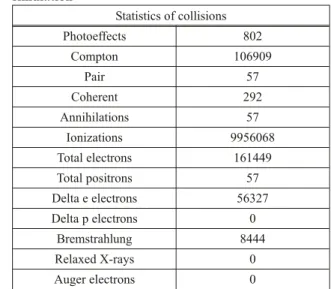
In or der to un der stand the ef fects of the gamma ra di a tion on the photodiode and the amount of de pos -ited en ergy, the Monte Carlo sim u la tion of pho ton trans port through a PIN photodiode has been used (tabs. 1 and 2, and fig. 3). In each zone of photodiode (tab. 1) and in al most ev ery layer (fig. 3), de pos ited en -ergy per in put par ti cle is high enough to dis place the lat tice atom i. e. to cre ate the va cancy. Ta ble 2 shows sta tis tics of col li sions in photodiode dur ing gamma ra
-di a tion. Each ef fect sep a rately (photoeffect, Compton, pair, PKA, va cancy, etc.) causes the ion iza tion of the at oms. Num ber of all in di vid ual ef fects is neg li gi ble com pared to the num ber of ion iza tions (tab. 2) so it could be as sumed that the most of ion iza tions has been cre ated by va can cies i. e. the num ber of va can cies cre -ated by gamma ir ra di a tion is sig nif i cant. Be cause of these va can cies and the va can cies cre ated by the neu -tron, the ra di a tion (divacancies) are caus ing the photocurrent in creas ing af ter neu tron ir ra di a tion and an neal ing that fol lows it [1].
For this re search, the longterm iso ther mal an neal ing at the room tem per a ture was used. The va can -cies and the in ter sti tials are quite mo bile in sil i con at the room tem per a ture and hence are re ferred to as an un sta ble de fects. Af ter va cancy in tro duc tion by ir ra di -a tion, v-a c-an cies move through the l-at tice -and form more sta ble de fects, such as divacancies and va cancyim pu rity com plexes. When elec tri cal prop er -ties are mon i tored dur ing this de fect re ar range ment (or an neal ing) pro cess, a de crease in the effectiveness of the dam age with in creas ing time is typ i cally ob served [27-30]. Moll [31] de scribes the en hance ment of the effective dop ing con cen tra tion for the lon ger an neal -ing times. This phe nom e non Feick [32] ob served at room tem per a ture. Dur ing the pro cess of an neal ing de fects clusterize and some elec tri cal in ac tive de fects be -come ac tive in a clus ter.
So, dur ing the com bined gamma and neu tron ra -di a tion a higher con cen tra tion of -divacanacies oc curs. Be cause of that, the an neal ing pro cess can par tially im -prove the elec tri cal char ac ter is tics of the photodiode dis turbed by gamma ra di a tion. This ef fect was not ev i -dent in the cases of sin gle gamma or neu tron ra di a tion. If there were not va can cies and other ef fects caused by gamma ra di a tion, neu tron ra di a tion would not be able to cause the photocurrent en hance ment. Only neu tron ir -ra di a tion ap plied af ter gamma -ra di a tion, causes the photocurrent en hance ment i. e. par tially im proves the char ac ter is tics of photodiodes dam aged by gamma ra -di a tion.
CONCLUSIONS
ex posed to gamma ra di a tion which causes the de te ri o -ra tion of their char ac ter is tics, this may be one way for a par tial re pair of dam age and im prove ment of the char ac ter is tics. This is spe cially im por tant for de tec tors work ing in hos tile con di tions, both from the fi -nan cial and tech no log i cal point of view, since it could en hance their work ing life time in such en vi ron ment.
ACKNOWLEDGEMENT
The Min is try of Ed u ca tion, Sci ence and Tech no -log i cal De vel op ment of Re pub lic of Ser bia sup ported this work un der con tracts 171007.
AUTHOR CONTRIBUTIONS
The o ret i cal anal y sis as car ried out by D S. Nikoli} and A. I. Vasi}. Ex per i ments were car ried out by D. S. Nikoli}, A. I. Vasi}, Dj. R. Lazarevi}, and M. D. Obrenovi}. All of the au thors have an a lyzed and dis cussed the re sults. The manu script was writ ten by D. S. Nikoli} and A. I. Vasi}. The fig ures were pre -pared by D. S. Nikoli}.
REFERENCES
[1] Watts, S. J., et al., A New Model for Gen er a tionRe
com bi na tion in Sil i con De ple tion Re gions af ter Neu -tron Ir ra di a tion, IEEE Trans ac tion on Nu clear Sci -ence, 43 (1996), 6, pp. 2587-2594
[2] Mohamed, B., et al., Ex per i men tal Mea sure ments of Some Op to el ec tronic De vices be fore and af ter Gamma Ir ra di a tion, Jour nal of Mi cro waves and Op to el ec tronic, 3 (2004), 4, pp. 1-12
[3] Kovalyuk, Z. D., et al., Ef fect of Gamma Ra di a tion on the Prop er ties of InSe Photodiodes, Tech ni cal Phys ics Let ters, 31 (2005), 5, pp. 359-360
[4] Vujisi}, M., Sim u lated Ef fects of Pro ton and Ion Beam Ir ra di a tion on Ti ta nium Di ox ide Memristors, IEEE Trans ac tions on Nu clear Sci ence, 57 (2010), 4, pp.
1798-1804
[5] Vujisi}, M., et al., Ra di a tion Hard ness of COTS
EPROM and EEPROM, Ra di a tion Ef fects and De fects in Sol ids, In cor po rat ing Plasma Sci ence and Plasma Tech nol ogy, 165 (2010), 5, pp. 362-369
[6] Al ex an der, D. R., Tran sient Ion iz ing Ra di a tion Ef fects in De vices and Cir cuits, IEEE Trans ac tion on Nu clear Sci ences, 50 (2003), 3, pp. 565-582
[7] Takagi, T., Noda, J., Gamma-Ray Ir ra di a tion Ef fects in Light-Emit ting Di ode and Photodiodes for Fi ber Op tics,
IEEE Trans ac tion Nu clear Sci ences, 32 (1985), pp.
4453-4459
[8] Barnes, C. E., The Ef fects of Ra di a tion on Op to el ec -tronic De vices, Proc., SPIE Fi ber Op tics in Ad verse Enviroments, 721 (1986), pp. 18-25
[9] Shockley, W., Read, W. T., Sta tis tics of the
Recombinations of Holes and Elec trons, Phys i cal Re -view, 87 (1952), 5, pp. 835-842
[10] Racko, J., et al., Cou pled De fect Level Re com bi na tion in the P-N Junc tion, Jour nal of Elec tri cal En gi neer ing, 62 (2011), 6, pp. 355-358
[11] Stankovi}, K., In flu ence of the Plain-Par al lel Elec trode Sur face Di men sions on the Type A Mea sure ment Un -cer tainty of GM Coun ter, Nucl Technol Radiat, 26
(2011), 1, pp. 39-44
[12] Doli}anin, ]., et al., Statistisal Treat ment of Nu clear
Count ing Re sults, Nucl Technol Radiat, 26 (2011), 2, pp.
164-170
[13] Stankovi}, K., et al., Sta tis ti cal Anal y sis of the Char ac ter is tics of Some Ba sic MassPro duced Pas sive Elec tri -cal Cir cuits Used in Mea sure ments, Mea sure ment, 44
(2011), 9, pp. 1713-1722
[14] Vujisi}, M., Stankovi}, K., Osmokrovi}, P., A Sta tis ti cal Anal y sis of Mea sure ment Re sults Ob tained from Non -lin ear Phys i cal Laws, Ap plied Math e mat i cal Mod el ing, 35 (2011), 7, pp. 3128-3135
[15] Ili}, R. D., FOTELP-2K10, Pho tons, Elec trons and
Pos i trons Monte Karlo Trans port Sim u la tion, http://www.vinca.rs/~rasa/hop8.htm, Bel grade, 2009 [16] Zeynali, O., et al.,Study of Ra di a tion Ef fects of Nu
-clear High En ergy Par ti cles on Elec tronic Cir cuits and Meth ods to Re duce Its De struc tive Ef fects, Jour nal of Mod ern Phusics, 2 (2011), 12, pp. 1567-1573 [17] Korde, R., et al., The Ef fect of Neu tron Ir ra di a tion on
Sil i con Photodiodes, IEEE Trans ac tions on Nu clear Sci ence, 36 (1989), 6, pp. 2169-2175
[18] HolmesSiedle, A., Ad ams, L., Hand book of Ra di a -tion Ef fects, Ox ford Sci ence Pub li ca -tion, 1993 [19] Mes sen ger, G. C., Ash, M. S., The Ef fects of Ra di a
-tion on Elec tronic Sys tems, 2nd ed., Van Nostrand
Reinhold, New York, USA, 1991
[20] Sporea, D. G., et al., Compartive Study of
Gamma-Ray, Neu tron and Elec tron Beam Ir ra di ated In dex-Guided La ser Di odes, Ra di a tion and Its Ef fects on Com po nents and Sys tems, RADECS 2005, 8th Eu
-ro pean Con fer ence on 2005, pp. PA3-1 - PA3-9 [21] Chen, W. M., et al., Di rect Ob ser va tion of Intercenter
Charge Trans fer in Dom i nant Nonradiative Re com bi na -tion Chan nels in Sil i con, Phys i cal Re view Let ters, 67
(1991), 14, pp. 1914-1917
[22] Frens, A. M., et al., Ob ser va tion of Rapid Di rect Trans
-fer be tween Deep De fects in Sil i con, Phys i cal Re view Let ters, 72 (1994), 18, pp. 2939-2942
[23] ***, Atomic & Ion Col li sions in Sol ids and at Sur faces: The ory, Sim u la tion and Ap pli ca tions, Cam bridge, (Ed. Smith, R.) Uni ver sity Press, Cam bridge, UK, 1997 [24] Nastasi, M., Mayer, J., Hirvonen, J., IonSolid In ter ac
-tions – Fun da men tals and Ap pli ca -tions, Cam bridge Uni ver sity Press, Cam bridge, GB, 1996
[25] Perlado, J. M., et al., Anal y sis of Dis place ment Cas -cades and Thresh old Dis place ment En er gies in Beta-SiC, Jour nal of Nu clear Ma te ri als, 276 (2000), 1-3, pp. 235-242
[26] El-Azab, A., Ghoniem, N., Mo lec u lar Dy nam ics Study of the Dis place ment Thresh old Sur faces and the Sta bil ity of Frenkel Pairs in Beta-Sic, Jour nal of Nu clear Ma te ri als, 191 (1992), pp. 1110-1114
[27] Mes sen ger, G. C., A Sum mary Re view of Dis place ment Dam age from High En ergy Ra di a tion in Semi -con duc tors and Semi -con duc tor De vices, Pro ceed -ings, First Eu ro pean Con fer ence on Ra di a tion and Its Ef fects on De vices and Sys tems, RADECS 91, La Grande-Motte, France, Sep tem ber 9-12, 1991, pp. 35-40
[28] Hauser, J. R., Kerns, S. E., Cir cuit Re lated Is sues Due to Ra di a tion in Hos tile En vi ron ments, Jour nal of Elec tronic Ma te ri als, 19 (1990), 7, pp. 671-688
[29] Gorlov, M. I., Litvinenko, D. A., An neal ing of Ra di a tion and Elec tro staticDis charge Dam ages in Semi con -duc tor De vices, Rus sian Mi cro elec tron ics, 31 (2002),
[30] Srour, J. R., Mar shall, C. J., Mar shall, P. W., Re view of Dis place ment Dam age Ef fects in Sil i con De vices,
IEEE Trans ac tions on Nu clear Sci ence, 50 (2003), 3,
pp. 653-670
[31] Moll, M., Ra di a tion Dam age in Sil i con Par ti cle De tec tors – Mi cro scopic De fect and Mac ro scopic Prop er ties, Ph. D. the sis, DESYTHE SIS1999040, De -cem ber 1999, Uni ver sity of Ham burg, Germany
[32] Feick, H., Ra di a tion Tol er ance of Sil i con Par ti cle De tec tors for HighEn ergy Phys ics, Ph. D. thesis, In ter nal Re port, DESY F35D 9708, Au gust 1997, Uni -ver sity Ham burg, Germany
Re ceived on Sep tem ber 26, 2012 Ac cepted on March 11, 2013
Dejan S. NIKOLI], Aleksandra I. VASI], \or|e R. LAZAREVI], Marija D. OBRENOVI]
MOGU]NOSTI POBOQ[AWA I-U KARAKTERISTIKE PIN FOTODIODA O[TE]ENIH GAMA ZRA^EWEM
U ovom radu se prikazuje pona{awe PIN fotodioda nakon ozra~ivawa gama zracima i neutronima. Razli~iti tipovi PIN fotodioda eksponirani su prvo gama zracima, a onda neutronima. Prime}eno je da je fotostruja nakon ozra~ivawa neutronima vi{a, nego pre ozra~ivawa, {to nije u skladu sa teorijom o efektima neutronskog zra~ewa na poluprovodnike. Da bi se objasnilo ovo pona{awe fotodioda, kori{}ena je Monte Karlo simulacija transporta fotona kroz materijal. Pretpostavka je da su mogu}i uzroci pove}awa struje defekti u poluprovodniku, izazvani gama ozra~ivawem i uticajem neutronskog zra~ewa na ove defekte. Ovi rezultati mogu se objasniti me|uprostornim kretawem naelektrisawa izme|u defekata koji su u neposrednoj blizini jedni drugima. Ciq ovog rada je da se istra`e mogu}a poboq{awa I-U karakteristika PIN fotodioda, odnosno fotodetektora, o{te}enih gama zracima.
![Fig ure 1. Sche matic di a gram of Schokley-Read-Hall the ory and intercentre charge trans fer gen er a tion pro cesses [1, 9]](https://thumb-eu.123doks.com/thumbv2/123dok_br/17295429.248293/2.894.464.789.910.1098/sche-matic-schokley-read-hall-intercentre-charge-cesses.webp)