SEN SI TIV ITY OF RADFET FOR GAMMA AND
X-RAY DOSES USED IN MED I CINE
by
Mili} M. PEJOVI] 1*, Svetlana M. PEJOVI]2, 3, Dragan STOJANOV 3, 4, and Olivera F. CIRAJ-BJELAC 5
1
Fac ulty of Elec tronic En gi neer ing, Uni ver sity of Niš, Niš, Ser bia 2
Saarland Uni ver sity Clinic, Hom burg, Ger many 3
Fac ulty of Med i cine, Uni ver sity of Niš, Niš, Ser bia 4
In sti tute of Ra di ol ogy, Uni ver sity of Niš, Niš, Ser bia 5
Vin~a In sti tute of Nu clear Sci ence, Uni ver sity of Bel grade, Bel grade, Serbia
Sci en tific pa per DOI: 10.2298/NTRP1403179P
In this pa per, the re sults of ra di a tion sen si tive field ef fect tran sis tors (Al-gate p-chan nel metalox idesemi con duc tor field ef fect tran sis tors) sen si tiv ity to gamma and Xray ir ra di a -tion are pre sented. Ra di a -tion fields were cre ated us ing 60Co source for three dose ranges (0-1 Gy, 0-5 Gy, and 0-50 Gy), as well as X-ray unit of 280 kVp spec trum for a sin gle dose range from 0 to 5 Gy. The sen si tiv ity was char ac ter ized by the thresh old volt age shift, de ter -mined from reader cir cuit mea sure ments, as a func tion of ab sorbed ra di a tion dose. It was shown that for the three dose ranges of gamma ra di a tion, as well as for the X-ray range from 0 Gy to 5 Gy there is ap prox i mately a lin ear de pend ence be tween thresh old volt age shift DV
T and ra di a tion dose D. The ap pli ca tion of pos i tive bias of +5 V at the RADFET gate dur ing ir -ra di a tion, for these -ranges of gamma -ra di a tion, also for X--ray dose -range, leads to the in crease in DV
T and also, ap prox i mately a lin ear de pend ence be tween DVT and D, is es tab lished. More over, it was shown that the sen si tiv ity of RADFET is much higher in the case of Xray ir ra di a -tion then in the case of gamma-ray ir ra di a -tion for the same dose range.
Key words: RADFET, gamma-ray ir ra di a tion, X-ray ir ra di a tion, thresh old volt age shift, ra di a tion dose
IN TRO DUC TION
Pchannel metalox idesemi con duc tor field ef fect tran sis tors (MOSFET) also known as ra di a tion sen si tive field ef fect tran sis tors (RADFET), or pMOS do -sim e ters have shown to be a suit able de tec tors for var i ous ap pli ca tions, rang ing from med i cal ap pli ca tions in di ag nos tic ra di ol ogy and ra dio ther apy to syn -chro tron ra di a tion and space do sim e try [1-5]. A ma jor ad van tage of the RADFET as a ra di a tion de tec tor is that the ra di a tionsen si tive re gion, the ox ide film un der -neath the alu mi num tran sis tor gate, is of a small vol ume [6, 7]. The sens ing vol ume is much smaller com pared to in te gral dose mea sur ing de vices such as ion iza tion cham ber, semi con duc tor di ode or thermoluminescent do sim e ter [8]. At ten tion is thus be ing turned to the use of RADFET es pe cially were the de tec tor has to be in -serted into a con fined space as a cath e ter [9, 10]. This prop erty of the RADFET also makes it at trac tive for mea sur ing in the high gra di ent ra di a tion field where the gra di ent mostly de pends on a sin gle space co or di nate,
like re solv ing dose pro files of X-ray mi cro beams or depth dose dis tri bu tion. How ever, the dis ad van tages of RADFET in clude the need for cal i bra tion in dif fer ent ra di a tion fields, rel a tively low res o lu tion (start ing from about 0.01 Gy) and non-re us abil ity. On the other hand, the lat ter prop erty can be con sid ered as an ad van tage, as it pro vides a per ma nent dose re cord. Some ear lier in -ves ti ga tions [11] have shown the pos si bil ity of RADFET re use, in clud ing our re cent in ves ti ga tions [12, 13].
The con cept of a RADFET is based on the build-up of pos i tive ox ide charge in the gate re gion when ex posed to ion iz ing ra di a tion. The elec tri cal sig -nal used as a dosimeteric pa ram e ter is the thresh old volt age. This pa ram e ter ex hib its a shift when RADFET is ir ra di ated. Thresh old volt age is the gate-source volt age (VGS) nec es sary to in duce in ver -sion be tween the sources and drain ter mi nals, which leads to a flow of con stant cur rent be tween these ter -mi nals [14]. The ba sic mech a nisms re spon si ble for thresh old volt age shift have been pre vi ously dis cussed else where [15-19]. It is shown that their be hav ior is a con se quence of the fol low ing mech a nisms: (1) elec
tronhole pair gen er a tion, (2) elec tronhole re com bi -na tion, (3) hole trans port, (4) deep hole trap ping, and (5) ra di a tionin duced in ter face and ox ide traps for ma -tion. As for many de tec tors, they need to be cal i brated against an ac cu rate dosimetric ref er ence, such as an ion iza tion cham ber trace able to an ac cepted do sim e try cal i bra tion lab o ra tory. Usu ally a RADFET is op er ated in in te gral mode, where the dose is de ter mined from the shift in thresh old volt age be fore and af ter it is ir ra di ated. In this case, the ef fect of fad ing and/or a tem -per a ture er ror can be sig nif i cant if long time elapses be tween ir ra di a tions, or tem per a ture changes oc cur be tween the ini tial and fi nal read out [20].
EX PER I MEN TAL DE TAILS
RADFET which are an ac ro nym for ra di a tion sen si tive field ef fect tran sis tors [21] with 1 mm thick gate ox ide spe cially de signed to mea sure ra di a tion doses (RADFET Tyn dall Na tional In sti tute, Cork, Ire -land) were used. The lay out of the sin gle chip is given else where [22]. The chip size is 1 mm ´ 1 mm, and there are two 300/50 and two 690/15 de vices on the chip. The num bers 300/50 and 690/15 rep re sent the width and length of RADFET chan nels, re spec tively. One 300/50 and one 690/15 de vices have four ter mi -nals, bulk, drain, gate, and source. The other de vices can be treated as two ter mi nal de vices be cause their gates and drains as well as their bulks and sources are joined to gether. Two ter mi nal de vices can be eas ily used in reader cir cuit con fig u ra tion. The tran sis tors ox ide was grown at 1000 °C in dry ox y gen and an -nealed for 15 min utes at 1000 °C in ni tro gen. The post metallization an neal ing was per formed at 440 °C in form ing gas for 60 min utes (for more de tails see [23] ). In the ex per i ment RADFET were di vided in eight groups. Two RADFET groups were ir ra di ated by gamma-rays orig i nat ing from 60Co in the ra di a tion
dose ranges from 0 Gy to 1 Gy with out gate bias (all ter mi nals were grounded) and with a pos i tive gate bias Virr = +5 V, re spec tively. Other two RADFET groups were ir ra di ated by gamma-rays orig i nat ing from 60Co
in the ra di a tion dose ranges from 0 to 5 Gy with out gate bias and Virr = +5 V, re spec tively. Two RADFET groups were ir ra di ated by gamma-rays orig i nat ing from 60Co in the ra di a tion dose ranges from 0 to 50 Gy
with out gate bias and with a pos i tive gate bias Virr = =.+5 V, re spec tively. Ir ra di a tion fa cil ity used was a teletherapy co balt source CIRUS-TS (CIS Alcyon Biointernational, France) with ac tiv ity of 230 TBq (1.9.1999). The last two MOSFET groups were ir ra di -ated with X-rays with mean en ergy of 140 keV (280 kVp) in the ra di a tion dose range from 0 Gy to 5 Gy, with out gate bias and gate bias Virr = +5 V, re spec -tively. In this case, ir ra di a tion was per formed us ing an X-ray gen er a tor MG 320 (Philips, The Neth er lands) with nom i nal tube volt age of 320 kVp. Beam qual ity
used for ir ra di a tion was gen er ated us ing a tube volt age of 280 kVp, in her ent fil tra tion of 4 mm Al and ad di -tional fil tra tion of 3.0 mm Cu, which cor re sponds to the first half-value layer of 18 mm Al or 3.6 mm Cu. Ir ra di a tion was per formed in the Sec ond ary Stan dard Do sim e try Lab o ra tory of the Vin~a In sti tute of Nu -clear Sci ence, Vin~aBel grade, Ser bia. All mea sure ments were con ducted in a cli matecon trolled lab o ra -tory en vi ron ment with am bi ent tem per a ture of 20 ±
0.20 °C. The air kerma at the ref er ence point was mea -sured with a cal i brated vented 0.6 cm3 ion iza tion
cham ber (Model 30012, PTW, Freiburg, Ger many) and electrometer Unidos (PTW, Freiburg, Ger many). The cal i bra tion of the cham ber in terms of air kerma for all ra di a tion qual i ties had been per formed at the Sec ond ary Stan dards Do sim e try Lab o ra tory of the In -ter na tional Atomic En ergy Agency (Vi enna, Aus tria), to pro vide trace abil ity to In ter na tional Bu reau of Weights and Mea sures (BIPM). Ir ra di a tion in co balt beam qual ity was per formed at dose rate of 192 mGy/min nor mal ized to 1 m form the source, so ir ra di -a tion time r-ang ing 8 to 42 min w-as used to -achieve doses of 1050 Gy at ir ra di a tion dis tance of 40 cm, re -spec tively. Sim i larly, dose rate in X-ray beam qual ity was 72 mGy/min at 1 m, which cor re sponds to ir ra di a -tion time rang ing from 14 to 70 min to achieve doses of 1-5 Gy, re spec tively.
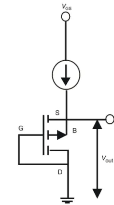
In or der to de tect thresh old volt age shift DVT, thresh old volt age be fore ir ra di a tion VT0, and thresh old volt age af ter ir ra di a tion VT were de ter mined, i. e., [24]. The thresh old volt age was de ter mined with de vices in the socalled reader cir cuit con fig u ra tion, whose elec -tric scheme is shown in fig. 1. In this ar range ment, a RADFET is treated as two ter mi nal de vices. Through the chan nel a steady cur rent ID = 10 mA is es tab lished and the volt age Vout which cor re sponds to this cur rent
is then mea sured. This volt age rep re sents thresh old volt age. Reader cir cuit con fig u ra tion pro vides fast and ac cu rate read out of RADFET thresh old volt age with -out any com plex elec tronic or logic cir cuits around the de tec tors of the RADFET ([23] for more de tails). This value of the cur rent was se lected be cause it was close to the zero tem per a ture co ef fi cients for our de vices. Namely, when reader cir cuit char ac ter is tics are mea -sured at dif fer ent tem per a tures, all of them in ter sect for the cur rent value of ap prox i mately 10 mA. Thus, the VT read out at 10 mA is tem per a ture in de pend ent. RADFET were read out im me di ately af ter each ir ra di -a tion, i. e., the time in ter val be tween each suc ces sive ir ra di a tion was less than a min ute.
Reader cir cuit mea sure ments were per formed by Keithley 4200 semi con duc tor char ac ter iza tion sys tem (SCS). The sys tem is equipped with three me -dium-power source mea sur ing units (4200 SMU). The source mea sur ing units have four volt age ranges (200 mV, 2 V, 20 V, and 200 V) and three cur rent re -gions (100 A, 100 mA, and 1 A). One of the source-mea sur ing units is equipped with a preamp-lifier for mea sur ing very small cur rents (in the or der of 1 pA).
RE SULTS
Fig ure 2 shows the de pend ence of thresh old volt age shift DVT on gamma-ra di a tion dose D in the 0 Gy to 1 Gy range for Virr = 0 V and Virr = +5 V. It can be seen that gate bias of +5 V leads to larger change in
DVT with the dose in crease then in the case when there is no bias on the gate.
De pend ence be tween DVT and D can be ex -pressed as DVT = ADn [24], where A is the con stant and
n is the de gree of lin ear ity de pend ing on the elec tric field, ox ide thick ness, and ab sorbed ra di a tion dose. Ide ally, this de pend ence is lin ear, i. e., n = 1, where A
rep re sents the sen si tiv ity DVT/ D. Sym bols in fig. 2 rep re sent DVT val ues from RADFET reader cir cuit mea sure ments while the solid lines are de ter mined by fit ting the data with ex pres sion DVT = ADn for n = 1. It
was shown that the val ues of cor re la tion co ef fi cients r2
are 0.99 for both Virr = 0 V and Virr = +5 V, re spec -tively. Hav ing that the cor re la tion co ef fi cients are very close to one, it can be as sumed that there is a lin ear de -pend ence be tween DVT and D, so that the sen si tiv ity
DVT/D is the same in the whole in ter val.
Thresh old volt age shift DVT for gamma and X-ray ir ra di a tion dose D in the 0 Gy to 5 Gy range for Virr = 0 V and Virr = +5 V is pre sented in figs. 3 and 4, re spec tively.
It can be seen that DVT in crease is much higher in the case when RADFET are ir ra di ated with X-rays then in the case of gammarays ir ra di a tion and this is a con -se quence of dif fer ent pho ton en er gies. Namely, X-rays beam qual ity used was gen er ated with tube volt age of Fig ure 2. RADFET thresh old volt age shift de pend ence
on gamma-ray ir ra di a tion dose in 0-1 Gy range with out gate bias and with gate bias Virr = +5 V
Fig ure 3. RADFET thresh old volt age shift de pend ence on gamma-ray ir ra di a tion in 0-5 Gy range with out gate bias and with gate bias Virr = +5 V
280 kVp with cor re spond ing half value layer of 18 mm Al, mean en ergy of 140 keV, while gammarays pho -tons orig i nated from 60Co. It is known that 60Co in each
dis in te gra tion emits b– par ti cles and two pho tons of en
-ergy 1.17 MeV (99.86%) and 1.33 MeV (99.98%), trans form ing it self into 60Ni. These two pho tons with
dif fer ent en er gies are usu ally con sid ered as av er age, with pho ton en ergy of 1.25 MeV. Due to dif fer ent pho -ton en er gies of X and gamma rays, dif fer ent in ter ac tion mech a nisms dom i nantly oc cur in the RADFET gate ox -ide, which fur ther lead to ra di a tion-in duced in ter face and ox ide traps for ma tion. On the ba sis of the atomic num ber as a func tion of pho ton en ergy [25] it can be con cluded that both pho to elec tric ef fect and Compton scat ter ing are oc cur ring, how ever their con tri bu tion to the to tal in ter ac tion co ef fi cient is dif fer ent, as pho to -elec tric ef fect con trib utes more at lower en er gies, whereas Compton scat ter ing dom i nates at higher en er gies. There fore, for co balt pho tons (1.25 MeV) the pri -mary ion iz ing mech a nism is Compton ef fect, but in the area of low and me dium-pho ton en ergy of X-rays there is a mixed in flu ence of Compton scat ter ing and photo-ef fect.
Fit ting of ex per i men tal data for gamma ra di a tion dose range from 0 Gy to 5 Gy (fig. 3) gives cor re la tion co ef fi cients of 0.99 for both Virr = 0 and Virr = +5 V. Cor re la tion co ef fi cients for the case when MOSFET are ir ra di ated with X-rays in the 0 Gy to 5 Gy range (fig. 4) are 0.96 and 0.95 for Virr = 0 V and Virr = +5 V, re spec tively, so it shows that the lin ear ity be tween DVT and D is sat is fac tory for prac ti cal ap pli ca tions.
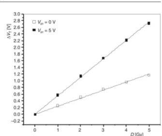
Fig ure 5 shows DVT = f(D) de pend ence for dose range from 0 Gy to 50 Gy for Virr = 0 V and Virr = +5 V. Fit ting of ex per i men tal data gives the lin ear cor re la -tion co ef fi cients o f 0.98 and 0.97 for Virr = 0 V and Virr = +5 V, re spec tively. It can be con cluded that in this dose range there is also an ap prox i mately lin ear de -pend ence be tween DVT and D.
Com par ing re sults be tween gammaray ir ra di a tion for dose range from 0 Gy to 50 Gy (fig. 5) with re -sults for X-ray ir ra di a tion for dose range from 0 Gy to 5 Gy (fig. 4) shows that DVT for gamma-ray ir ra di a tion dose of 50 Gy and X-ray ir ra di a tion dose of 5 Gy are ap prox i mately the same for Virr = 0 V. For Virr = + 5 V,
DVT for X-ray ir ra di a tion is about 4 V higher than in the gamma-ray ir ra di a tion case. It can be con cluded that RADFET are much more sen si tive to Xray ir ra di -a tion.
DIS CUS SIONS
Many in ves ti ga tions [17-19, 26-33] have shown that the ex po sure of MOS com po nents to gamma and X-ray ir ra di a tion leads to the in crease of elec tri cal charge in the in su lat ing gate ox ide (net pos i tive ox ide trapped charge) and in ter face charge (in ter face traps). The do sim e try of ion iz ing ra di a tion us ing MOS tran -sis tor is based on the mea sure ment of pos i tive ox ide trapped charge in the gate ox ide Qox and in ter face traps Qit. Qox leads to the shift of ID-VG curve to wards more neg a tive volt age. The in ter face charge Qit also con trib -utes to this shift and in ad di tion, re duces the slope of the lin ear part of the curve due to deg ra da tion of the car rier mo bil ity in the tran sis tors chan nel [21].
The thresh old volt age VT given by [34]
V V Q Q
C V V
T T0 ox it ox
T T
= - + = 0+D
where Cox is the ox ide ca pac i tance per area unit. In the
case of p-chan nel MOSFET (RADFET) both Qox and
Qit are pos i tive and add to de fine DVT, i. e., both ef fects
re sult in a neg a tive shift of the thresh old volt age. The phys i cal mech a nisms lead ing to the cre ation of pos i tive ox ide trapped charge and in ter face traps dur ing ir ra di a tion have been stud ied for many years [20, 35, 36] and here we will dis cuss only the main fea -tures re quired for their un der stand ing. Namely, gamma and X-ray ir ra di a tion gen er ates elec tron-hole pairs in the ox ide, and the frac tion of them which es -cape ini tial re com bi na tion is ac cel er ated to ward the elec trodes. Un der pos i tive gate bias, elec trons mi grate to ward the gate and holes be ing slower mi grate to ward SiO2/Si in ter face. Dur ing the mi gra tion some holes can be cap tured in de fects in SiO2 struc ture, which are mainly lo cated near SiO2/Si in ter face, and be have as hole traps. The re sult is a buildup of a rel a tively sta ble pos i tive ox ide trapped charge den sity. Prob a bly as a re sult of the lib er a tion of hy dro gen ions in ox ide dur -ing ir ra di a tion, in ter face traps are also cre ated [25].
Our ear lier in ves ti ga tions [24] have shown that the ir ra di a tion of RADFET with gammaray ir ra di a -tion leads to the for ma -tion of pos i tive ox ide trapped charge which is ten times greater than in ter face traps den sity. Be cause of that, the in flu ence of in ter face traps can be ne glected in thresh old volt age shift Fig ure 5. RADFET thresh old volt age shift de pend ence
change. It is known that the num ber of cre ated pos i tive ox ide trapped charge rises with the num ber of holes which avoid the re com bi na tion with the elec trons and this pro cess de pends on gate po lar iza tion dur ing ir ra -di a tion, Virr. For Virr = 0 (figs. 2 to 5), the elec tric field in the ox ide is only a con se quence of the work func tion dif fer ence be tween the gate and sub strate (the zero-bias con di tions are equal to the gate bias of 0.3 V), so the prob a bil ity for elec tronhole re com bi na -tion is higher than in the case when Virr = 5 V. Namely, for Virr = 5 V the large num ber of holes will es cape the ini tial re com bi na tion, which in creases the prob a bil ity for the cre ation of pos i tive ox ide trapped charge. Such in crease is man i fested through the in crease of thresh -old volt age shift for the same value of ir ra di a tion dose, which can be clearly seen in figs. 2 to 5.
Larger val ues of DVT when RADFET were ir ra -di ated by X-rays (fig. 4) then in the case when they were ir ra di ated by gammarays (fig. 3) are a con se -quence of dif fer ent for ma tion of pos i tive ox ide trapped charge den sity. Dur ing gamma ir ra di a tion the pri mary ion iz ing mech a nism is Compton's ef fect and its in flu ence on for ma tion of ox ide trapped charge den sity is con sid er ably smaller than in the case of X-rays ir ra di a tion when there is a mixed in flu ence of Compton's ef fect and photoef fect. It should be em pha sized that our re sults (figs. 3 and 4) are in agree ment with ear lier in ves ti ga tions of clin i cal semi con -duc tor do sim e try sys tem (CSDS) MOSFET ir ra di ated by X-rays whose pho ton en er gies were 36 keV, 123 keV, and 1.4 Mev [36]. It was shown that the de crease of X-rays ir ra di a tion en ergy leads to the in crease of thresh old volt age, so it can be con cluded that the photo-ef fect con tri bu tion to the pos i tive ox ide trapped charge for ma tion is much big ger than the con tri bu tion of Compton's ef fect. Such con clu sion is in agree ment with the re sults pre sented in figs. 4 and 5, where it can be seen that thresh old volt age shift for gammarays ir -ra di a tion up to 50 Gy dose and X--rays ir -ra di a tion dose of 5 Gy are ap prox i mately the same for Virr = 0 V, while for Virr = 5 V thresh old volt age shift for Xrays ir ra di a -tion is about 4 V higher than in the case of gamma-ray ir ra di a tion.
CON CLU SIONS
The sen si tiv ity of RADFET man u fac tured in Tyn dall Na tional In sti tute, Cork, Ire land with 1 mm thick gate ox ide to gamma-ray ir ra di a tion for ra di a tion dose ranges 0-1 Gy, 0-5 Gy, and 0-50 Gy as well as for X-ray ir ra di a tion for ra di a tion dose range 0-5 Gy has been in ves ti gated. Be cause av er age pho ton en ergy is 1.25 MeV the pri mary ion iza tion mech a nism is Compton's scat ter ing. The pho ton en ergy of Xray ir -ra di a tion used in our ex per i ments was 140 keV, so there was a mixed in flu ence of Compton's scat ter ing and photo-ef fect. The sen si tiv ity of stud ied de vices
was based on thresh old volt age shift de ter mined from reader cir cuit mea sure ments. These re sults show that for con sid ered dose ranges of gamma and X-rays there is ap prox i mately a lin ear de pend ence be tween thresh -old volt age shift and ab sorbed dose, which shows that the sen si tiv ity for con sid ered ra di a tion dose ranges can be ex pressed as a ra tio be tween thresh old volt age shift and ra di a tion dose. The ap pli ca tion of pos i tive bias on the gate, Virr = +5 V, leads to the sen si tiv ity in -crease of these de vices. The re sults have also shown that the sen si tiv ity is greater when RADFET are ir ra di -ated by X-rays than by gamma-rays for the same dose range. The ex pla na tion for such be hav ior can be found in the fact that mixed in flu ence of Compton's scat ter -ing and photo-ef fect leads to the for ma tion of greater den sity of pos i tive ox ide trapped charge than in the case when only Compton's ef fect ex ists.
Due to the high sen si tiv ity of con sid ered com po nents to Xrays ir ra di a tion it can be ex pected their sat -is fac tory sen si tiv ity for lower ra di a tion doses than the ones used in this pa per. Our fur ther in ves ti ga tions will be fo cused to lower doses of X-rays ir ra di a tion, be low 1 cGy in or der to in ves ti gate the RADFET ap pli ca tion in dose range used in ra di ol ogy.
AC KNOWL EDGE MENTS
The Min is try of Ed u ca tion, Sci ence and Tech no log i cal De vel op ment of the Re pub lic of Serbia, sup -ported this work fi nan cially through the pro ject No. 171007.
AU THOR CON TRI BU TIONS
The o ret i cal anal y sis was car ried out by M. M. Pejovi}, ex per i ments were car ried out by M. M. Pejovi}, S. M. Pejovi}, and O. F. Ciraj-Bjelac. All of the au thors have an a lyzed and dis cussed the re sults. The manu script was writ ten by M. M. Pejovi}, S. M. Pejovi}, and O. F. CirajBjelac. The fig ures were pre -pared by M. M. Pejovi}.
REF ER ENCES
[1] Bower, M. W., Hintenlang, D. E., The Char ac ter iza -tion of a Com mer cial MOSFET Do sim e ter Sys tem for Use in Di ag nos tic X-Ray, Health Phys., 75 (1998), 2, pp. 197-204
[2] Kron, T., et al., Dose Re sponse of Var i ous Ra di a tion De tec tors to Syn chro tron Ra di a tion, Phys. Med. Biol., 43 (1998), 11, pp. 3235-3259
[3] Peet, D. J., Pryor, M. D., Eval u a tion of a MOSFET Ra di a tion Sen sor for the Mea sure ment of En trance Sur face Dose in Di ag nos tic Ra di ol ogy, Br. J. Radiol., 72 (1999), 858, pp. 562-568
Thermoluminescence Do sim e ters for use in Di ag nos -tic Ra di ol ogy, Appl. Radiat. Isot., 57 (2002), 6, pp. 883-891
[5] Marcie, S., et al., In vivo Mea sure ments with MOSFETS Detectrors in Oropharynx and Nanopharynx Intesity-Mod u lated Ra di a tion Ther apy, Int. J. Radiat. Oncol. Biol. Phys., 61 (2005), 5, pp. 1603-1606
[6] Holmes-Siedle, A., The Space-Charge Do sim e ter – Gen eral Prin ci ples of a New Method of Ra di a tion De -tec tion, Nucl. Instr. Meth ods, 121 (1974), 1, pp. 169-179
[7] Rosenfeld, A. B., et al., MOSFET Do sim e ters: Role of En cap su la tion of Dosimetric Char ac ter is tics in Mixed Gamma-Neu tron and Megavoltage X-Ray Field, IEEE Trtans. Nucl. Sci., 42 (1995), 6, pp. 1870-1877
[8] Kaplan, G. I., et al., Im proved Spa tial Res o lu tion by MOSFET Do sim e try of an X-Ray Microbeam, Med. Phys., 27 (2000), 1, pp. 239-244
[9] Hughes, R. C., et al., Min ia ture Ra di a tion Do sim e ter for in vivo Ra di a tion Mea sure ments, Int. J. Radiat. Oncol. Biol. Phys., 14 (1988), 5, pp. 936-967
[10] Glad stone, D. J., et al., A Min ia ture MOSFET Ra di a -tion Do sim e ter Probe, Med. Phys., 21 (1994), 11, pp. 1721-1728
[11] Kelleher, A., et al., In ves ti ga tion Into the Re use of pMOS Do sim e ters, IEEE Trans. Nucl. Sci., 41 (1994), 3, pp. 445-451
[12] Pejovi}, M. M., et al., Suc ces sive GammaRay Ir ra di -a tion -and Cor re spond ing Post-Ir r-a di -a tion An ne-al ing of pMOS Do sim e ters, Nucl Technol Radiat, 27
(2012), 4, pp. 341-345
[13] Pejovi}, M. M., Pejovi}, M. M., Jaksi}, A. B., Re sponse of pMOS Do sim e ters on GammaRay Ir ra di a -tion Dur ing its Re-Use, Ra di a tion Pro tec tion Do sim e -try, 155 (2013), 4, pp. 394-403
[14] Carvajal, M. A., et al., Ther mal Drift Re duc tion with Mul ti ple Bias Cur rent for MOSFET Do sim e ters,
Phys. in Med. and Biol., 56 (2011), 12, pp. 3535-3550
[15] Soubra, M., Cygler, J., Mackay, G., Eval u a tion of a Dual Bias Metal-Ox ide-Sil i con-Semi con duc tor Field Ef fect Tran sis tor De tec tor as Ra di a tion Do sim e ter,
Med. Phys., 21 (1994), 1, pp. 567-572
[16] Thomson, I., Thomson, R. E., Berndt, L. P., Ra di a tion Do sim e try with MOS Sen sor, Nucl. Appl. Technol., 6
(1984), 1, pp. 121-124
[17] Benedetto, J. M., Boesch, H. E., McLean, F. B., Dose En ergy De pend ence of In ter face Trap For ma tion in
60
Co and X-Ray En vi ron ments, IEEE Trans. Nucl. Sci., 35 (1988), 6, pp. 1260-1264
[18] Shaneyfelt, M. R., Fleetwood, D. M., Hughes, K. L., Charge Yield for Co balt60 and 10 keV XRay Ir ra di -a tion of MOS De vices, IEEE Trans. Nucl. Sci., 38
(1991), 6, pp. 1187-1193
[19] Oldham, T. R., McLean, F. B., To tal Ion iz ing Dose Ef -fect in Mos Ox ides and De vices, IEEE Trans. Nucl. Sci., 50 (2003), 3, pp. 483-499
[20] Rosenfeld, A. B., et al., Fea si bil ity Study of On line High-Spa tial-Res o lu tion MOSFETS Do sim e try in Static Pulsed X-Ray Ra di a tion Fields, IEEE Trans. Nucl. Sci., 48 (2001), 6, pp. 2061-2068
[21] Hughes, R., The ory of Re sponse of Ra di a tion Sens ing Field Ef fect Tran sis tors, J. Appl. Phys., 58 (1985), 3, pp. 1375-1380
[22] Pejovi}, S., et al., Char ac ter is tics of MOSFET Suit -able for Use in Ra dio ther apy, Appl. Radiat. and Iso -topes, 77 (2013), pp. 44-49
[23] Jaksi}, A., et al., GammaRay Ir ra di a tion and PostIr -ra di a tion Re sponse of High Dose Range RADFET,
IEEE Trans. Nucl. Sci., 49 (2002), 3, pp. 1356-1363
[24] Pejovi}, M. M., Pejovi}, M. M., Jaksi}, A. B., Con tri -bu tion of Fixed Ox ide Traps to Sensitivy of pMOS Do sim e ters Dur ing Gamma Ray Ir ra di a tion and An -neal ing at Room and El e vated Tem per a ture, Sen sors and Ac tu a tors, A 174 (2012), pp. 85-90
[25] Risti}, G. S., In flu ence of Ion iz ing Ra di a tion and Hot Car ried In jec tion on Metal-Ox ide-Semi con duc tor Tran sis tors, J. Phys. D: Appl. Phys., 41 (2008), 2, 023001
[26] Sarrabayrouse, G., Gessinn, F., Thick Ox ide MIOS Tran sis tors for Ion iz ing Ra di a tion Dose Mea sure -ment, Radioprotection, 29 (1994), 4, pp. 557-572
[27] Oldham, T., Ion iz ing Ra di a tion Ef fects in MOS Ox ides, Ad vances in Solid State Elec tron ics and Tech -nol ogy Se ries, Springer; World Sci en tific, 1999
[28] Huges, H. L., Benedent, J. M., Ra di a tion Ef fects and Hard en ing of MOS Tech nol ogy: De vices and Cir -cuits, IEEE Trans.Nucl. Sci., 50 (2003), 3, pp. 500-520
[29] Johnston, A. H., Super Re cov ery of the Dose Dam age in MOS De vices, IEEE Trans. Nucl. Sci., 31 (1984), 6, pp. 1427-1433
[30] Benedetto, J. M., Boesh, H. E., The Re la tion ship Be -tween 60Co and 10 keV XRay Dam age in MOS De -vices, IEEE Trans. Nucl. Sci., 33 (1986), 6, pp. 1318-1323
[31] Dozier, C. M., et al., An Eval u a tion of Low-En ergy XRay and Co balt60 Ir ra di a tions of MOS Tran sis -tors, IEEE Trans. Nucl. Sci., 34 (1987), 6, pp. 1535-1539
[32] Beutler, D. E., et al., Vari a tions in Semi con duc tor De vice Re sponse in a Me dium En ergy XRay DoseEn -hanc ing En vi ron ment, IEEE Trans. Nucl. Sci., 34
(1987), 6, pp. 1544-1550
[33] Vuki}, V. Dj., Osmokrovi}, P. V., Fail ure of Neg a tive Volt age Reg u la tor in Me diumPho tonEn ergy x Ra di -a tion Fields, Mi cro elec tron ics Re li abil ity, 54 (2014), 1, pp. 79-89
[34] Dasgupta, A., et al., Dose en hance ment and Re duc -tion in SiO2 and High-k MOS In su la tors, IEEE Trans. Nucl. Sci., 57 (2010), 6, pp. 3463-3469
[35] Fleetwood, D. M., et al., Com par i son of En hanced De vice Re sponse and Pre dicted X-Ray Dose En -hance ment Ef fects on MOS Ox ides, IEEE Trans. Nucl. Sci., 35 (1988), 6, pp. 1265-1271
[36] Cheung, T., Butson, M. J., Yu, P. K. N., En ergy De pend ence Cor rec tions to MOSFET Dosimetric Sen si -tiv ity, Austras. Phys. Eng. Sci. in Med., 32 (2009), 1, pp. 16-20
Mili} M. PEJOVI], Svetlana M. PEJOVI], Dragan STOJANOV, Olivera F. CIRAJ-BJELAC
OSETQIVOST RADFET TRANZISTORA ZA DOZE GAMA I X-ZRA^EWA KOJE SE KORISTE U MEDICINI
U ovom radu prikazani su rezultati vezani za osetqivost RADFET-ova na gama i X-zra~ewe. Kao izvor gama zra~ewa kori{}en je 60Co i ozra~ivawe je ura|eno za tri opsega doza (0-1 Gy, 0-5 Gy, i 0-50 Gy) kao i izvor X-zra~ewa 280 kVp za opseg doza od 0-5 Gy. Karakterizacija osetqivosti je vr{ena na osnovu pomeraja napona praga DV
T., odre|ena iz merewa napona praga u
jednoj ta~ki strujno-naponske karakteristike, kao funkcije apsorbovane doze D. Pokazano je da za
tri opsega doze gama zra~ewa kao i za opseg doze X-zra~ewa od 0 do 5 Gy postoji pribli`no linearna zavisnost izme|u DV
T i D. Primena pozitivne polarizacije na gejtu od +5 V RADFET-ova dovodi do
porasta vrednosti DV
T i tako|e postoji pribli`no linerna zavisnost izme|u DVT i D. Osim toga je
pokazano da je osetqivost RADFET-ova znatno ve}a u slu~aju ozra~ivawa X-zracima nego gama zracima za isti opseg doze.