w w w . a j e r . o r g Page 159
American Journal of Engineering Research (AJER)
e-ISSN : 2320-0847 p-ISSN : 2320-0936
Volume-02, Issue-07, pp-159-166
www.ajer.org
Research Paper Open Access
Total Harmonics Distortion Investigation in Multilevel Inverters
Avinash verma, Ruchi shivhare, Sanjeev gupta
Samrat ashoka technological engineering institute Vidisha(mp) india 464001
Abstract: The multilevel began with the three level inverter. Use of conventional two – level pulse width
modulation (PWM) inverter provide less distorted current and voltage but at cost of higher switching losses due to high switching frequency. Multilevel inverter are emerging as a viable alternative for high power , medium voltage application. This paper compare total harmonics distortion in three level and five level diode clamped multilevel inverter. Diode –clamped three phase topology is considered for study. A sinusoidal PWM technique is used to control the switches of the inverter. Simulation study confirms the reduction in harmonics distortion.
Keywords: - Harmonics , multilevel inverter , pulse width modulation , Total harmonics distortion
I. INTRODUCTION
Wave form of practical inverter are non- sinusoidal and contain certain harmonics. for low –and medium power application, square wave or quasi – square wave form voltage may be acceptable but for high – power application sinusoidal waveform with low distortion are required. Harmonics content present in the output of a dc to ac inverter can be eliminated either by using a filter circuit or by employing pulse width modulation (PWM) techniques. Use of filter has the disadvantage of large size and cost, whereas use of PWM techniques reduces the filter requirement to a minimum or to zero depending on the type of application. Traditional two level high frequency PWM inverter have some drawback, such as production of common mode voltage.[1-3]
Multilevel inverter have found better counter to the conventional two – level pulse width modulation inverter to overcome the above problems. In addition they offer the advantage of less switching stress on eachdevice for high voltage high power application , with a reduced harmonics content at low switching frequency.
A comparative study of five level and seven level diode clamped capacitor clamped and cascade inverter has been presented in [4]. The effect of a passive LC filter on the inverter performance was studied. simulation result indicated reduction in total harmonics distortion (THD) by using higher number of level. This paper investigates five level inverter and seven level inverter diode clamped three phase inverter on the basic of the THD .an extensive simulation study to optimize the THD content in the line voltage have been presented in this paper.
II. RELATED WORK
In recent years, industry has begun to demand higher power equipment, which now reaches the megawatt level.Controlled AC drives in themegawatt range are usually connected to the medium-voltage network. Today, it ishard to connect a single power semiconductor switch directly to medium voltage grids. For these reasons, a newfamily of multilevel inverters has emerged as the solution for working with higher voltage levels. Depending onvoltage levels of the output voltage, the inverters can be classified as two-level inverters and multilevel inverters.
w w w . a j e r . o r g Page 160
introduced controlschemes for DC capacitor voltages equalization in diode clamped multilevel inverter basedDSTATCOM.Monge et al [4] proposed multilevel diode clamped converter for photovoltaic generators with independentvoltage control of each solar array. Renge and Suryawanshi [5] developed five level diode clamped inverter toeliminate common mode voltage and reduce dv/dt in medium voltage rating induction motor drives. HideakiFujita and Naoya Yamashita [6] discussed performance of a diode clamped linear amplifier. Hatti et al [7]proposed a 6.6-KV transformer less motor drive using a five level diode clamped PWM inverter for energysavings of pumps and blowers. Srinivas in [8] discussed uniform overlapped multi carrier PWM for a six leveldiode clamped inverter. EnginOzdemir et al [9] introduced fundamental frequency modulated six level diodeclamped multilevelinverter for three phase standalone photovoltaic system. BerrezzekFarid and BerrezzekFarid[10] made a study on new techniques of controlled PWM inverters. Anshumanshukla et al [11] proposed flyingcapacitor based chopper circuit for DC capacitor voltage balancing in diode clamped multilevel inverter. Thisliteraturesurvey revealsfew papers only on various PWM techniques and hence this work presents a novelapproach for controlling the harmonics of output voltage of chosen MLI employing sinusoidal switchingstrategies. Simulations are performed using MATLAB-SIMULINK. Harmonics analysis and evaluation ofperformance measures for various modulation indices have been carried out and presented.
III. MULTILEVEL INVERTER
Neutral Point-Clamped Inverter:
A three-level diode-clamped inverter is shown in Fig. 2(a). In this circuit, the dc-bus voltage is split into three levels by two series-connected bulk capacitors, C1 and C2. The middle point of the two capacitors n can be defined as the neutral point. The output voltage van has three states: Vdc/2, 0, and -Vdc/2. For voltage level Vdc/2, switches S1 and S2 need to be turned on; for -Vdc/2, switches S1’ and S2’ need to be turned on;
and for the 0 level, S2 and S1’ need to be turned on.
The key components that distinguish this circuit from a conventional two-level inverter are D1 and
D1’. These two diodes clamp the switch voltage to half the level of the dc-bus voltage. When both S1 and S2
turn on, the voltage across a and 0 is Vdc i.e., va0 =Vdc. In this case, D1’ balances out the voltage sharing between S1’ and S2’ with S1’ blocking the voltage across C1 and S2’ blocking the voltage across C2. Notice
that output voltage van is ac, and va0 is dc. The difference between van and va0 is the voltage across C2, which isVdc /2. If the output is removed out between a and 0, then the circuit becomes a dc/dc converter, which has three output voltage levels: Vdc ,Vdc/2, and 0.
(a) seven-level. (b) Five-level. Figure 2 clamped multilevel inverter circuit topologies.
Considering that m is the number of steps of the phase voltage with respect to the negative terminal of the inverter, then the number of steps in the voltage between two phases of the load k isk = 2m+1 (1) and the number of steps p in the phase voltage of a three-phase load in wye connection isp = 2k – 1. (2)
w w w . a j e r . o r g Page 161
bus consists of four capacitors, C1, C2, C3, and C4. For dc-bus voltage Vdc, the voltage across each capacitor is Vdc/4, and each device voltage stress will be limited to one capacitor voltage level Vdc/4 through clamping diodes.To explain how the staircase voltage is synthesized, the neutral point n is considered as the output phase voltage reference point. There are five switch combinations to synthesize five level voltages across a and n. 1) For voltage level Van = Vdc/2, turn on all upper switches S1– S4.
2) For voltage level Van = Vdc/4, turn on three upper switches S2–S4 and one lower switch S1’.
3) For voltage level Van = 0, turn on two upper switchesS3 and S4 and two lower switches S1’ and S2’.
4) For voltage level Van = –Vdc/4, turn on one upper switch and three lower switches S1’–S3’. 5) For voltage level Van = –Vdc/2, turn on all lower switches S1’–S4’.
Four complementary switch pairs exist in each phase. The complementary switch pair is defined such that turning on one of the switches will exclude the other from being turned on. In this example, the four
complementary pairs are (S1, S1’), (S2, S2’), (S3, S3’), and (S4, S4’).
TABLE I. SWITHCING STATES OF THE FIVE LEVEL INVERTER
Va0 S1 S2 S3 S4 S1’ S2’ S3’ S4’
V5=Vdc 1 1 1 1 0 0 0 0
V4=3Vdc/4 0 1 1 1 1 0 0 0
V3=Vdc/2 0 0 1 1 1 1 0 0
V2=Vdc/4 0 0 0 1 1 1 1 0
V1= 0 0 0 0 0 1 1 1 1
Although each active switching device is only required to block a voltage level of Vdc/(m-1), the clamping diodes must have different voltage ratings for reverse voltage blocking. Using D1’of Fig. 2(b) as an
example, when lower devices S2’ ~ S4’ are turned on, D1’ needs to block three capacitor voltages, or 3Vdc/4. Similarly, D2 and D2’ need to block 2Vdc/4, and D3 needs to block 3Vdc/4. Assuming that each blocking diode
voltage rating is the same as the active device voltage rating, the number of diodes required for each phase will be (m-1) (m-2). This number represents a quadratic increase in m. When m is sufficiently high, the number of diodes required will make the system impractical to implement. If the inverter runs under PWM, the diode reverse recovery of these clamping diodes becomes the major design challenge in high-voltage high-power applications.
IV. MODULATIONTECHNIQUE
SPWM:
Several multicarrier techniques have been developed to reduce the distortion in multilevel inverters, based on the classical SPWM with triangular carriers. Some methods use carrier disposition and others use phase shifting of multiple carrier signals [7], [8], [9].
The sinusoidal PWM compares a high frequency triangular carrier with three sinusoidal reference signals, known as the modulating signals to generate the gating signals for the inverter switches. This is basically an analog domain technique and is commonly used in power conversion with both analog and digital implementation.The smallest distortion is obtained when the carriers are shifted by an angle of �= 360°⋰
�� = 120°. A very common practice in industrial applications for the multilevel inverter is the injection of a
third harmonic in each cellto increase the output voltage [6], [10]. Another advantageous feature of multilevel SPWM is that the effective switching frequency of the load voltage is three (NC=3) times the switching frequency of each cell, as determined by its carrier signal. This property allows a reduction in the switching frequency of each cell, thus reducing the switching losses.
Proposed SPWM for NPC Multilevel Inverter:
In the SPWM scheme for two-level inverters, each reference phase voltage is compared with the triangular carrier and the individual pole voltages are generated, independent of each other. The SPWM technique, for multilevel inverters, involves comparing the reference phase voltage signals with a number of symmetrical level-shifted carrier waves for PWM generation [11]. It has been shown that for an n-level inverter, n-1 level-shifted carrier waves are required for comparison with the sinusoidal references [11].
w w w . a j e r . o r g Page 162
V. RESULT & ANALYSIS
The simulation is carried out using MATLAB/Simulink. Simulation circuit of three phase level NPC isshown in Figure.1. Detailed simulation circuit of each phase is shown in Figure.2. Input is 100V DC .levels inverter output voltage and current in a phase are shown in Figure3. and Figure4.respectively. The phasevoltages and currents in three phase inverter are shown in Figure5. and Figure6.respectively. The line voltagesare shown in Figure7.. The circuit is analyzed for RL load. The FFT analysis result is shown in Figure.8
MATLAB Model for Five level DCMLI:-
The simulation is carried out using MATLAB/Simulink. Simulation circuit of three phase Five level shown in figure 5.13. Detailed simulation circuit shown is figure 5.14. input is 100 v dc. five level inverter output voltage. The FFT analysis is result.
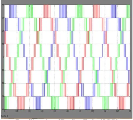
Simulation Result for PWM generating logic PDPWM technique:
Figure 1Simulation Resultfor PWM generating logic Five Level PDPWM technique ( ma = 1 and mf =20)
Simulation Result for Output voltage generated by PDPWM technique:
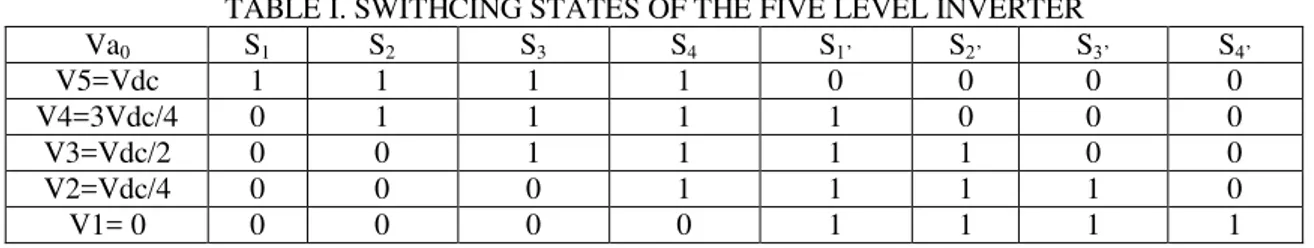
w w w . a j e r . o r g Page 163 Phase voltage of Three Phase PDDCMLI:
Figure 3Phase voltage of Three Phase Five Level DCMLI
FFT plot for Simulation Result output voltage of PDPWM technique
w w w . a j e r . o r g Page 164 Simulation Result for Seven level PWM generating logic PDPWM technique
Figure5Simulation Result for PWM generating logic PDPWM technique
Simulation Result for Output voltage generated by PDPWMtechnique
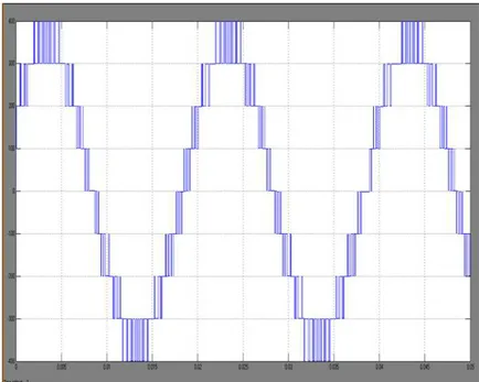
w w w . a j e r . o r g Page 165 Phase voltage of Three Phase PDDCMLI
Figure 7 Phase voltage of Three Phase PDDCMLI
FFT plot for Simulation Result output voltage of PDPWM technique
Figure 8 FFT plot for Simulation Result output voltage of PDPWM technique
TABLE % THD comparison for different LEVELS
It has shown that decrease in voltage THD in moving from three levelstoseven level inverter. It has shown that number of level increase output voltage THD is decrease.
Output Voltage level of NPCI THD Fundamental Component
Five level 16.30 346.5
w w w . a j e r . o r g Page 166
VI. CONCLUSION
A SPWM technique is proposed for three-level and five-level NPC inverter. The main feature of the modulation scheme lies in its ability to eliminate the harmonics in the inverter output voltages.The harmonic content and THD of the inverter output voltage produced by the three and five levels are compared and it seamless for five level diode clamped inverter compared three level diode clamped multilevel inverter.
REFERENCES
[1] Xiaoming Yuan and Ivo Barbi “Fundamentals of a New Diode Clamping Multilevel Inverter”, IEEETrans.on Power Electronics, Vol.15, No.4, 2000, pp.711-718.
[2] O. Bouhali, B. Francois, E. M. Berkouk, and C. Saudemont, “DC Link Capacitor Voltage Balancing in a Three-Phase Diode Clamped Inverter Controlled by a Direct Space Vector of Line-to-Line Voltages”, IEEE Trans. on Power Electronics, Vol.22, No.5, 2007, pp.1636-1648.
[3] AnshumanShukla, ArindamGhosh and Avinash Joshi, “Control Schemes for DC Capacitor Voltages Equalization in Diode-Clamped Multilevel Inverter Based DSTATCOM”, IEEE Trans. on Power Delivery, Vol.23, No.2, 2008, pp.1139-1149.
[4] Sergio BusquetsMonge, Joan Rocabert Pedro Rodriguez, Salvador Alepuz and JosepBordonau,
“Multilevel Diode Clamped Converter for Photovoltaic Generators With Independent Voltage Control
of Each Solar Array”, IEEE Trans. on Industrial Electronics, Vol.55, No.7, 2008, pp.2713-2723. [5] Mohan M. Renge and Hiralal M. Suryawanshi, “Five-Level Diode Clamped Inverter to Eliminate
Common Mode Voltage and Reduce dv/dt in Medium Voltage Rating Induction Motor Drives”, IEEE Trans. on Power Electronics, Vol.23, No.4, 2008, pp.1598-1607.
[6] Hideaki Fujita, and Naoya Yamashita, “Performance of a Diode-Clamped Linear Amplifier”, IEEE Trans. on Power Electronics, Vol.23, No.2, 2008, pp.824-831.
[7] NatchpongHatti, Kazunori Hasegawa and Hirofumi Akagi, “A 6.6-KV Transformer less Motor Drive Using a Five-Level Diode- Clamped PWM Inverter For Energy Savings of Pumps and Blowers”, IEEE Trans. on Power Electronics, Vol.24, No.3, 2009, pp.796-803.
[8] S.Srinivas, “Uniform Overlapped Multi-Carrier PWM for a Six-Level Diode Clamped Inverter”, International Journal of Electrical and Electronics Engineering , 2009, pp.763-768.
[9] EnginOzdemir, SuleOzdemir and Leon M. Tolbert, “Fundamental-Frequency-Modulated Six-Level Diode-Clamped Multilevel Inverter for Three-Phase Stand-Alone Photovoltaic System” IEEE Trans. on Power Electronics, Vol.56, No.11, 2009, pp.4407-4415.
[10] BerrezzekFarid and BerrezzekFarid, “A Study of New Techniques of Controlled PWM Inverters”, European Journal of Scientific Research, ISSN 1450-216X, Vol.32, No.1, 2009, pp.77-87.