Analysis of the Inhomogeneous Barrier in In/p-Si Schottky Contact and Modified Richardson Plot
J.M. Dhimmar, H.N. Desai, B.P. Modi*
Department of Physics, Veer Narmad South Gujarat University, Surat, Gujarat, India
(Received 27 January 2016; revised manuscript received 09 June 2016; published online 21 June 2016)
The current-voltage (I-V) characteristics of In/p-Si Schottky barrier contact were measured over the temperature range 230-360 K with interval of 10 K. The calculated zero bias barrier height (bo) and the
ideality factor (n) using thermionic theory show strong temperature dependence. The experimental values of
bo
and n for In/p-Si Schottky contact range from 0.70 eV and 1.91 (at 360 K) to 0.49 eV and 2.99 (at 230 K) respectively. The conventional Richardson plot exhibits nonlinearity at lower temperature. The Richardson constant determined from intercept at the ordinate of this experimental linear portion is the value of 2.07 10– 8 A/cm2K2 which is much lower than the theoretical value 32 A/cm2K2 for holes in p-type silicon. The
temperature dependence of Schottky barrier characteristics of the contact was interpreted on the basis of the existence of Gaussian distribution of the barrier height around a mean value due to barrier height inhomogeneties prevailing at the metal semiconductor interface. The modified
2 2 2 2
0 21
ln Is q 2k T versus
T
T
plot gives bo 1.17 eV and A* 31.16 A/cm2K2 with standard deviation
0 0.16 V.
Keywords: Zero bias barrier height, Schottky contact, Ideality factor, Modified Richardson plot, Standard deviation.
DOI: 10.21272/jnep.8(2).02006 PACS numbers: 73.30. + y, 73.20. – r
*[email protected]
1. INTRODUCTION
Metal-Semiconductor (M-S) contacts are found to be important research activity because the knowledge of barrier formation is still far from the complete despite the fact that they are work horse at many electronic applications like surge protection, high speed operation, microwave field effect transistors, radio frequency detectors, temperature sensors and solar cells etc. [1-4]. Although, M-S contacts have been used as research tool in the characterization of new semiconductor materials. In the information era, it is continuing need faster and complex systems to improve in device technology. Usually, the analysis of the characteristics I-V are linear in the semi-logarithmic scale at low voltages, but deviate noticeably from linearity due to the effect of parameters such as the series resistance, the interfacial layer and interface states [6-9]. The series resistance is only effective in the downward-curvature region (non linear region) of the forward I-V characteristics at large applied voltages but ideality factor and barrier height are effective through out the region of characteristics [10, 11]. This is because that the lining up process of energy bands in M-S junctions after contact are expected to depend on various charge transfer mechanisms, e.g. intrinsic surface states, metal induced gap states, impurities, microstructure defects,, crystallography and relative orientations of atoms at contact and across the interface [12, 13]. The performance and stability of
Schottky contact especially depend on the formation of insulator between M-S interface, inhomogeneties and series resistance. The analysis of the I-V characteristics of the Schottky contact based on thermionic emission theory typically, reveals an abnormal decrease of zero bias barrier height and increase in the ideality factor with decrease in temperature. [14-21]. The decrease in the barrier height at low temperatures leads to non-linearity in the Richardson’s plot, and is found to be non ideal. The theoretical studies based on the effect of a Gaussian distribution of Schottky barrier on the I-V characteristics have been also reported in literature [22-28].
In the present study the forward bias I-V characteristics of In/p-Si Schottky contact were measured over the temperature range of 220-360 K. The temperature dependent Schottky barrier height and ideality factor of the non ideal In/p-Si Schottky contact modified Richardson plot offers a good straight line over the entire temperature range [29]. The resultant temperature dependent non ideal Schottky contacts have been explained on the basis of the existence of a Gaussian distribution of the barrier heights around a mean value due to inhomogeneties at the M-S interface.
2. EXPERIMENTAL PROCEDURE
and washed with de-ionized water. After chemically etched with 4 : 1 : 3 solution of HNO3 : HF : NH4OH for
30 sec. till brown vapour appeared and then it was dipped for a minute in dilute solution of 1 : 9 HF : H2O
[30]. Finally, the wafer was rinsed in deionized water for 30 sec. The thick aluminum back contact (thickness of 3000 Å) was thermally evaporated by means of a tungsten filament onto the complete back of silicon crystal under pressure 1 10– 6 Torr. The low resistivity
ohmic back contact was made by using by an annealing treatment at 550 oC for 30 minutes in under pressure
1 10– 6 Torr. The Schottky contact was formed onto
front polished surface of silicon by evaporation of high purity soft indium metal dots with diameter of about 0.828 mm. The I-V measurements were performed by the use of a Keithly electrometer-614 and a programmable power supply in temperature range of 220-360 K using a temperature controlled cryostat.
3. RESULTS AND DISCUSSION
The forward bias I-V characteristics of the In/p-Si Schottky contact for wide temperature range of 220-360 K by step of 10 K are shown in Fig. 1. The forward current through a Schottky barrier contact at a forward bias (V≥ 3 kT/q) according to thermionic emission (TE) theory, is given by [31, 32]
exp 1 exp
s
qV qV
I I
nkT kT
(1)
where Is is the saturation current and is defined by
* 2exp bo
s
q
I AA T
kT
(2)
Where A is the effective diode area, A* is the
Richardson constant for p-type Si (A* 32 A cm– 2 K– 2), q is the electronic charge, V is the voltage across the diode, k is the Boltzman constant, T is the absolute temperature, bo the zero-bias barrier height and n is the ideality factor. The ideality factor is calculated using the slope of straight line region of the forward bias logarithmic characteristic I-V through relation
ln
q dV
n
kT d I
(3)
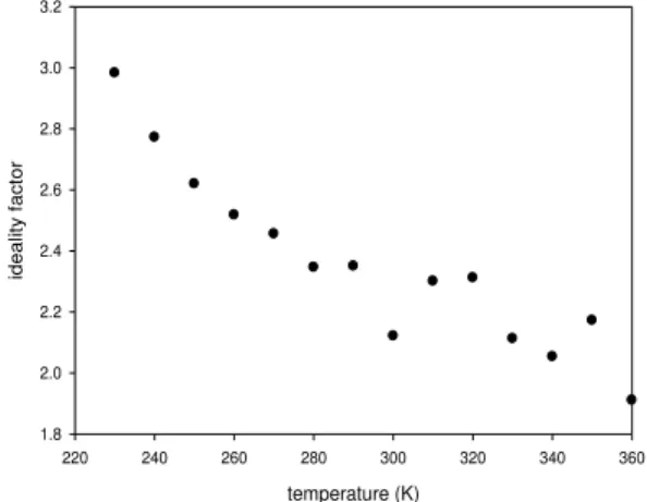
Where n is justified of conformity of pure thermionic emission. The variation of the experimental ideality factor at different temperatures is plotted in Fig. 2. As shown in the figure, an apparent increase in the ideality factor has been attributed to the effects such as inhomogeneities of thickness, non uniformity of the interfacial charges and insulator layer between metal and semiconductor. These give rise to an extra current such that the over all characteristics still remain consistent with the thermionic emission
V (V)
0.0 0.1 0.2 0.3 0.4 0.5
I (
A
)
1e-7 1e-6 1e-5 1e-4 1e-3
360 K 350 K 340 K 330 K 320 K 310 K 300 K 290 K 280 K 270 K 260 K 250 K 240 K 230K
Fig. 1 – The forward I-V characteristics for In/p-Si Schottky contact at different temperatures
The value of IS saturation current is determined from
the intercept of the plot lnI versus V in the temperature range of 220-360 K shown in Fig. 1. The calculated value Is
is used to determine zero bias barrier height bo is expressed as [31]:
* 2
ln bo
s
kT AA T
q I
(4)
The barrier height obtained under flat band condition is called the flat barrier height
bF
. Flat band barrier height is considered as the real fundamental quantity since the electric field in the semiconductor is zero under flat condition unlike in the case of zero bias barrier height. Also this eliminates the effect of the image force lowering that would affect the I-V characteristics and removes the influence of lateral inhomogeneity [34-35]. The flat-band barrier height bF is calculating from the experimental
ideality factor and zero bias barrier height bo by the following equation [36]:
1
ln VbF bo
A
N kT
n n
q N
(5)
Where NV is the effective density of states in the
valance band and NA is the carrier concentration of the
semiconductor (1016 cm– 3) used.
The value of zero bias barrier height (bo) and flat band barrier height (bF) are plotted as function of temperature
dependence of the flat band barrier height can be expressed as
0
bF T bF T T
(6)
where bFis the flat band barrier height extrapolated to
T 0 K and is its temperature coefficient. In Fig. 3, the fitting of bF(T) data in equation (6) provides
bF
(T 0) 1.07 eV and 3.130 10– 4 eV K– 1. This
experimental value of temperature coefficient of barrier height for the In/p-Si Schottky contact is good in agreement with temperature coefficient value of 4.73 10– 4 eV K– 1 for silicon [37].
temperature (K)
220 240 260 280 300 320 340 360
ideali
ty
f
ac
tor
1.8 2.0 2.2 2.4 2.6 2.8 3.0 3.2
Fig. 2 – Ideality factor with temperature for In/p-Si schottky contact
The Schmitsdorf, et al. [38] used Tung’s theoretical approach that there is a linear relation between the apparent zero bias barrier height and ideality factors. The variation of the apparent barrier height versus the ideality factor is shown in Fig. 4. As shown in the figure, there is linear relationship between the apparent effective barrier heights and the ideality factor of the contacts that can be explained by lateral inhomogeneties of the barrier heights in Schottky contacts [39-42]. The extrapolation of the apparent barrier height versus the ideality factor plot to n 1 has given a homogeneous Schootky barrier height
of approximately 1.11 eV. Thus, it can be said that the significant decrease of the zero bias barrier height and increase of the ideality factor towards decreasing temperature are possible caused by the barrier height inhomogeneties. It is seen to have good linearity and is a proof of applicability of the interfacial model [43]. The value of flat band barrier heights evaluated from here is found to be 1.07 eV.
To determine barrier height in another way by use of Richardson plot for reverse saturation current by taking natural logarithm of equation (2) rewritten as The Richardson constant is usually determinate from the
intercept of ln Is2 vs1
T T
plot. The conventional energy
temperature (K)
220 240 260 280 300 320 340 360
Z
er
ob
ias b
ar
ri
er
he
igh
t
an
d
F
lat
ba
nd
ba
rr
ier
he
igh
t
(eV
)
0.4 0.6 0.8 1.0 1.2 1.4
zero bias barrier height Flat band barrierheight
Fig. 3– Zero bias barrier height and flat band barrier height for In/p-Si schottky contact
ideality factor (n)
1.8 2.0 2.2 2.4 2.6 2.8 3.0 3.2 3.4
ap
pe
ar
an
t
ba
rr
ier
he
igh
t
0.4 0.5 0.6 0.7 0.8
y = - 0.218x + 1.1136
Fig. 4 – Linear variation of apparent barrier height vs ideality factor at different temperatures for In/p-Si Schottky contact
*2
ln Is ln AA q bo
KT T
(7)
variation of ln Is2 vs1
T T
plot is found to be non linear in the temperature-range measured as shown in Fig. 5. However,
thenln Is2 vs1
T T
gives a straight line as shown in Fig. 6. The activation energy from the experimental data are shown in Fig. 5 gives 0.12 eV and Richardson constant A* (2.07 10– 8 A/cm2 K2) which is much lower than the known value of p-
type silicon 32 A/cm2 K2. The deviation in the Richardson plots
may be due to the spatial inhomogeneous barrier heights and potential fluctuations at the interface that consist of low and high barrier areas. [44-47]. In other words, the current of the diode will flow preferentially through the lower barriers in the potential distribution. Horvath [47] explained that the A*
the barrier. The plot of modified nln Is2 vs1
T T
gives an
activation energy of 1.5 eV and Richardson constant 25.58 A/cm2 K2.
In real Schottky contact, the barrier heights vary over the contact area because of variations in the interfacial layer thickness and/or composition and also because of interfacial charges. For the correction the barrier height inhomogeneties have been obtained a modified value of the Richardson constant closer to the known value 32 A/cm2 K2. The inhomogeneous barrier
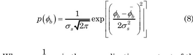
behaviour can be explained using an analytical potential fluctuation model [48-55]. The decrease in the barrier height with a decrease in temperature can be explained by the lateral distribution of barrier height if the barrier height has a Gaussian distribution analysis
of the barrier height values with a mean value
_
b
and standard deviationswhich can be given by [54, 55]
2
2
1 exp
2 2
b b
b
s s
p
(8)
Where 1
2 s
is the normalization constant of the
Gaussian barrier height distribution. The total value I(V) across Schottky contact containing a barrier inhomogeneties can be expressed as
b,
b bI V I V P d
(9)
Where I
b,V
is the current at a bias V for a barrier of height based on the ideal thermionic emission– diffusion theory and P
b is the normalized distribution function giving the probability of accuracy for barrier height. Substituting Eq. (2) for I
b,V
andEq. (8) for P
b in Eq. (9), obtain the current I(V)through the Schottky barrier at a forward bias V but with a modified barrier as [3]
sexp 1 expap
qV qV
I V I
n kT kT
With
* 2exp ap
s
q
I AA T
kT
(10)
Where nap and ap are the apparent ideality factor and the apparent barrier height respectively. With Gaussian distribution of barrier height at the interface due to homogeneities have shown that temperature variation at zero bias respectively is given by [56-58].
2_
0 2
so ap b
q T
kT
(11)
3 2
1 1
2 ap
q
n kT
(12)
It is believed that the mean value
_
b
and standard deviationsare linearly bias dependent of Gaussian
parameter such that bbo2Vandsso3V,
where 2 and3 are the voltage coefficients that may depend on temperature and they measure the voltage deformation of the barrier height distribution. Using the experimental data calculate nap and bo by Eqs. (3) and (4) at zero bias respectively, which should obey Eqs. (10) and (11). The plot of apversus 1/T (Fig. 7) should be a straight
line that gives bo 1.06 eV and o 0.16 V from the intercept and slope respectively. The standard deviation is a measure of the barrier inhomogenity. The lower value of
o
corresponds to more homogeneous barrier height [59]. The value of voltage coefficients 2 and3 are obtained
from the intercept and slope of the plot (Fig. 8) (2 1.11 V
and 3 – 0.017 V ). The linear behavior plot (Fig. 7 and 8) show that the ideality factor expresses the voltage deformation of the Gaussian distribution of the Schottky barrier contact. The value of standard deviation ofrom slope of this line is found to be 0.16 V.
The conventional Richardson plot is now modified by combining Eqs. (11) with (12) as follows
2 2 2 2
*0 2
ln Is q 2k T lnAA q bo
kT T
(13)
The plot of a modified 2
2 02 2 2
1
ln Is q 2k T vs
T
T
according to Eq. (13) should give a straight line with the slope directly yielding the mean bo(T 0) and the intercept ( lnAA*) at the ordinate determining Richardson
constant A* for a given diode area A.
Fig. 9 shows this modified plot gives values of bo(T 0) and A* as 1.17 eV and 31.16 A/cm2K2 respectively, without
using the temperature coefficient of the flat band barrier height. The value of bo(T 0) 1.17 eV from this plot is
nearly same as the value of bo(T 0) 1.06 eV from the
plot of apvs1
T
. However, Bhuiyan, Martinez and Esteve
[60] give a new Richardson plot of nln Is2 vs1
T T
1/T
0.0026 0.0028 0.0030 0.0032 0.0034 0.0036 0.0038 0.0040 0.0042 0.0044 0.0046
ln
(
Is
/T
2)
-27.0 -26.5 -26.0 -25.5 -25.0 -24.5 -24.0
y = -1387 x - 20.60
Fig. 5– Richardson plot of the ln Is2 vs1
T T
for In/p-Si Schottky contact
1/T
0.0026 0.0028 0.0030 0.0032 0.0034 0.0036 0.0038 0.0040 0.0042 0.0044 0.0046
n
ln
(Is
/T
2)
-90 -80 -70 -60 -50 -40
y = -17490 x + 0.323
Fig. 6 – The modified Richardson plot n ln Is2 vs1
T T
for In/p-Si Schottky contact
1/T
0.0026 0.0028 0.0030 0.0032 0.0034 0.0036 0.0038 0.0040 0.0042 0.0044 0.0046 0.0048
ap
pa
ren
t
ba
rr
ier
he
igh
t
0.45 0.50 0.55 0.60 0.65 0.70 0.75
y = -134.0 x + 1.061
Fig. 7 – Apparent barrier height vs 1/T for In/p-Si Schottky contact
It is found that the barrier height has a value of
around 1.06 eV from the plot of apvs1
T
which is
compared with the flat band barrier height 1.07 eV and the barrier height obtained from the modified
Richardson plot 1.17 eV and the standard deviation in barrier height is 0.16 V. Thus, the conformity to be quite satisfactory.
1/T
0.0026 0.0028 0.0030 0.0032 0.0034 0.0036 0.0038 0.0040 0.0042 0.0044 0.0046
n
-1-1
-0.70 -0.65 -0.60 -0.55 -0.50 -0.45
Fig. 8 – Variation (n1 1)vs1 T
for In/p-Si Schottky contact
1/T
0.0026 0.0028 0.0030 0.0032 0.0034 0.0036 0.0038 0.0040 0.0042 0.0044 0.0046
ln
(
Is
/T
2
)-1
/2
(q
/kT
)
2
-60 -55 -50 -45 -40 -35
y = -17490 x + 0.323
Fig. 9– The modified Richardson plot
2
2
1 1
ln 2
s o
I q
vs
kT T
T
for
In-pSi Schottky contact according to Gaussian distribution of barrier heights
4. CONCLUSION
Evaluation of non ideal Schottky contact is very complex. The I-V characteristics of In/p-Si Schottky contact were measured over the temperature range of 220-360 K. It can be interpreted on the basis of the TE theory with Gaussian distribution of the barrier height of bo(T 0) 1.17 eV and standard deviation o is found to be 0.16 V. The lower value
o
corresponds to more homogenous barrier height. In addition, the inhomogenity and potential fluctuations may be occurring as a result of inhomogeneties in the composition of interfacial oxide layer or thickness and non uniformity of interfacial charges. Furthermore, the experimental results of
ap
and nap fit very well for the theoretical equation related to
the Gaussian distribution of ap and nap. Again the
2
1 ln Is vs
T T
constant, but used Richardson Plot of n T
ln IS2 vs1T T
and modified Richardson plot obtained A* 25.58 A/cm2
K2 and 31.16 A/cm2K2 respectively Thus, modified
Richardson plot using Gaussian distribution of the barrier height is very nearer to the theoretical value 32 A/cm2K2
of holes in p-type silicon.
ACKNOWLEDGMENT
We thank to Dr. K.D. Patel and Prof. R. Srivastava, Department of Physics, Sardar Patel University, Vallabh Vidyanagar for meaningful discussion with this paper. These acknowledged with a deep sense of gratitude.
REFERENCE
1. E.H. Rhoderick, R.H. Williams, Metal-Semiconductor contacts (Clarendon Press: Oxford: 1988).
2. R.T. Tung, Appl. Phys. Rev.1, 0111304 (2014).
3. K Ejderha, N. Yildirim, A. Turat, Superlattice. Microstr.
47, 241 (2010).
4. S. Shankar Niak, V Rajgopal Reddy, Superlattice. Microstr.48, 330 (2010).
5. O. Gullu, A. Turat, J. Alloy. Compd.509, 571 (2011). 6. M.K. Hudait, S.B. Krupanidhi, Solid State Electron. 44,
1087 (2000).
7. M. Biber, M. Cakar, A. Turut, J. Mater. Sci.-Mater. Elect.
12, 575 (2001).
8. H. Kanbur, S. Altindal, A. Tataroglu, Appl. Surf. Sci.252, 1732 (2005).
9. S. Karatas, S. Alt1ndal, A. Turat, M. Cakar, Physica B 392, 43 (2007).
10.S.K. Cheung, N.W. Cheung, Appl. Phys. Lett. 49, 85 (1986).
11.A. Turat, M. Saglam, Physica B179, 285 (1992).
12.M.K. Hudait, S.P. Venkateswarlu, S.B. Krupanidhi, Solid State Electron. 45, 133 (2001).
13.J.P. Sullivan, R.T. Tung, M.R. Pinto, J. Appl. Phys. 70, 7403 (1991).
14.A. Gumus, A. Turit, N. Yalcin, J. Appl. Phys. 91, 245 (2002).
15.S. Altindal, S. Karadeniz, N. Tugluogiu, A. Tataroglu, Solid State Electron. 47, 1847 (2003).
16.S. Karatas, S. Altindal, M. Cakar, Physica B 357, 386 (2005).
17.M. Ozer, D.E. Yildiz, S. Alt1ndal, M.M. Bulbul, Solid State Electron. 51, 941 (2007).
18.M.K. Hudait, S.P. Venkateswarlu, S.B. Krupanidhi, Solid State Electron. 45, 133 (2001).
19.H. Korkuta, N. Yıldırıma, A. Turut, H. Dogan, Mater. Sci. Eng. B157, 48 (2009).
20.H. Altuntas, S. Altındal, H. Shtrikman, S. Özçelik, Microelectron. Reliability49, 904 (2009).
21.M. Sharma, S.K. Tripathi, J. Appl. Phys. 112, 024521 (2012).
22.S. Chand, Semicond. Sci. Technol. 17, L36 (2002). 23.H. Cetin, B. Sahin, E. Ayyildiz, A. Turat, Semicond. Sci.
Technol. 19, 1113 (2004).
24.M.E. Aydin, O. Gullu, N. Yild1r1m, Physica B 403, 131 (2008).
25.M. Saglm, A. Ates, B. Guzeldir, A. Astam, M.A. Y1ld1r1m, J. Alloy. Compd.480, 962 (2009).
26.M. Mamor, J. Phys. Condens. Matt.21, 335802 (2009). 27.I1bi1ge Dokme, Semesettin Altindal, M.M. Bulbul, Appl.
Surf. Sci.252, 7749 (2006).
28.W. Mtangi, F.D. Auret, C. Nyamhere, P.J. Janse van Rensburg, M. Diale, A. Chawanda, Physica B 404, 1092 (2009).
29.B.P. Modi, J. Nano- Electron. Phys. 3 No 1, 680 (2011).
30.M.M. Heyns, S. Verhaverbeke, M. Meuris, P.W. Merteus, H. Schmidt, M. Kubota, A. Phillpresian, K. Dillenbech, D. Grat, A. Schnegg, R. DeBlank, Mater. Res. Soc. Symp. Proc.315, 35 (1993).
31.S.M. Sze, Physics of Semiconductor Devices, 2nd Ed. (New York: Wiley Eastern: 1993).
32.S. Ashok, J.M. Borrego, R.J. Gutmann, Solid State Electron.
22, 621 (1979).
33.S. Duman, Semicond. Sci. Technol. 23, 075042 (2008).
34.S. Hardikar, M.K. Hudait, P. Modak, S.B. Krupanidhi, N. Padha, Appl. Phys. A68, 49 (1999).
35.A. Gumus, A. Turat, N. Yalcin, J. Appl. Phys.91, 245 (2002). 36.L.F. Wagner, R.W. Young, A. Sugerman, IEEE Electron. Dev.
Lett.4 No 4, 320 (1983).
37.H.C. Card, E.H. Rhoderick, J. Phys. D Appl. Phys. 4, 1589 (1971).
38.R.F. Schmitsdorf, T.U. Kampen, W. Mönch, J. Vac. Sci. Technol. B15, 1221 (1997).
39.R.T. Tung, Phys. Rev. B45, 1509 (1992).
40.S. Sankar Nair, V. Rajgopal Reddy, Adv. Mat. Lett.3 No 3, 188 (2012).
41.W. Monch, J. Vac. Technol. B17, 1867 (1999).
42.C. Temric, B. Bati, M. Saglam, A. Turut, Appl. Surf. Sci.172, 1 (2001).
43.R.F. Schmitsdorf, T.U. Kampen, W. Monch, Surf. Sci.324, 249 (1995).
44.J.H. Werner, H.H. Guttler, J.Appl. Phys. 69, 1522 (1991). 45.Y.P. Song, R.L. Van Merihaeghe, W.H. Lafiere, F. Cardon,
Solid State Electron. 29, 633 (1986).
46.S. Karatas, S. Alt1ndal, A. Turat, A. Ozmen, Appl. Surf. Sci.
217, 250 (2003).
47.Zs. Horvarth, Solid State Electron. 39, 176 (1996).
48.M.K. Hudait, P. Venkateswarlu, S.B. Krupanidhi, Solid-State Electron.45, 133 (2001).
49.S. Chand, Semicond. Sci. Technol.19, 82 (2004).
50.S. Zhu, R.L. Van Meirhaeghe, C. Detavernier, G.P. Ru, B.Z. Li, F. Cardon, Solid-State Commun.112, 611 (1999).
51.Ş.Altındal, S. Karadeniz, N. Tuğluoğlu, A.Tataroğlu, Solid-State Electron.47, 1847 (2003).
52.S. Zeyrek, Ş.Altındal, H.Yüzer, M.M.Bülbül, Appl. Surf. Sci.
252, 2999 (2006).
53.S. Zhu, R.L. Van Meirhaeghe, C. Detavernier, F. Cardon, G.P. Ru, X.P. Qu, B.Z. Li, Solid-State Elecron.44, 663 (2000). 54.O.S. Anilturkand, R. Turan, Solid-State Electron.44, 41 (2000). 55.S. Bandyopadhaya, A. Bhattacharya Andd, S.K. Sen,
J. Appl. Phys.85, 3671 (1999).
56.J.H. Werner, H.H. Guttler, Phys. Scr. T39, 258 (1991). 57.S. Karats, S. Altidnal, A. Turut, A. Ozmen, Appl. Surf. Sci.
217, 250 (2003).
58.A. Gumus, A. Turut, N. Yalcin, J. Appl. Phys. 91, 245 (2002). 59.R.T. Tung, Mater. Sci. Eng. R35, 1 (2001).