832 PACS numbers: 73.40.Qv; 85.30.Hi
EFFECT OF SERIES RESISTANCE AND INTERFACE STATE DENSITY ON ELECTRICAL CHARACTERISTICS OF Au/SiO2/n-GaN SCHOTTKY
DIODES
M. Siva Pratap Reddy1, B. Prasanna Lakshmi1, A. Ashok Kumar2, V. Rajagopal Reddy1
1 Sri Venkateswara University,
Tirupati - 517 502, Andhra Pradesh, India E-mail: [email protected]
2 Y.S.R Engineering College of Yogivemana University, Proddatur - 516 630, Andhra Pradesh, India
We have investigated the current-voltage (I - V) characteristics of (Au/SiO2/n-GaN) metal-insulator-semiconductor (MIS) Schottky diodes and compared with (Au/n-GaN) metal-semiconductor (MS) Schottky diode. The effect of SiO2 on the surface preparation of n-GaN (MIS) Schottky diode is analyzed. The extracted Schottky barrier height and ideality factor of the MS Schottky diode is found to be 0.79 eV and 1.45 respectively. It is observed that the Schottky barrier height increases to 0.86 eV and ideality factor decreases to 1.3 for MIS diode. The interface state density as determined by Terman’s method is found to be 3.79 × 10¹² and 3.41 × 1010 cm - 2 eV - 1 for the MS and MIS Schottky diodes, respectively. In addition, the values of series resistance (Rs) are determined using Cheung’s method. The I - V characteristics confirmed that the distribution of Nss, Rs and interfacial layer are important parameters that influence the electrical characteristics of MIS Schottky diodes.
Keywords: METAL-INSULATOR-SEMICONDUCTOR CONTACTS, SCHOTTKY BARRIER HIEGHT, IDEALITY FACTOR, INTERFACE DENSITIES.
(Received 04 February 2011)
1. INTRODUCTION
2. EXPERIMENTAL DETAILS
Si-doped GaN samples used in this study were grown by metal-organic chemical vapor deposition (MOCVD) on a c-plane Al2O3 substrate. The carrier concentration obtained by means of Hall measurements was
~ 4.07 × 1017 cm - 3. The n-GaN was first ultrasonically cleaned with warm trichloroethylene followed by acetone and methanol for 5 min each. This layer was then dipped into boiling aqua-regia [HNO3: HCl = 1:3] for 10 min to remove the surface oxides and then rinsed in deionized (DI) water. Ti (25 nm)/Al (100 nm) were deposited on a portion of the sample as ohmic contacts using an electron beam evaporation system under a vacuum pressure of 4 × 10 - 6 mbar. The samples were annealed at 650 °C in N
2 ambient for 3 min. First Au (50 nm) Schottky contact with a diameter of 0.7 mm were deposited through stainless steel mask using e-beam evaporation on one of the piece of GaN film. A 20 nm thick SiO2 layer was deposited on the other piece of GaN sample followed by 50 nm thick Au by electron beam evaporation system. Au evaporation processes were carried out in a vacuum coating unit at a pressure of about 5-6 × 10 – 6 mbar. The current-voltage (I-V), capacitance-voltage (C-V) characteristics of Au/n-GaN (MS) and Au/SiO2/n-GaN (MIS) Schottky contacts were measured using Keithley source measuring unit 2400 and automated DLTS (DLS-83D) system at room temperature.
3. RESULTS AND DISCUSSION
3.1 Current-voltage (I - V) characteristics
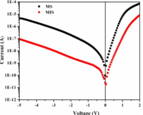
The current-voltage characteristics are used widely to study the performance of the Schottky contacts since they offer many important device parameters. Fig. 1 shows the forward and reverse biased curves of Au/n-GaN (MS) and Au/SiO2/n-GaN (MIS) Schottky diodes at room temperature. For forward bias and V > 3kT/q, the following equation describe the I-V characteristics of the Schottky diode according to the thermionic emission theory [7],
(
)
æ - ö
= ç ÷
è ø
exp s
s
q V R I
I I
nKT (1)
where saturation current Is is expressed by,
j
æ ö
= ç- ÷
è ø
** 2
exp
s b
q
I AA T
kT (2)
where q is the electronic charge, T the measurement temperature in Kelvin, n the ideality factor, A** the effective Richardson constant (by using an effective mass of 0.22 me for n-GaN, the value of A** is calculated to be 26.4 Acm - 2K -2), k the Boltzmann constant, Rs the series resistance, j
to electron traps localized at the GaN interface and associated with Ga vacancies created near the surface during the formation of insulating layer. Consequently it is clear that the different barrier heights could be due to modified-interface chemistry.
Fig. 1 - Typical current-voltage characteristics of the Au/n-GaN (MS) and Au/SiO2/n-GaN (MIS) diodes at room temperature
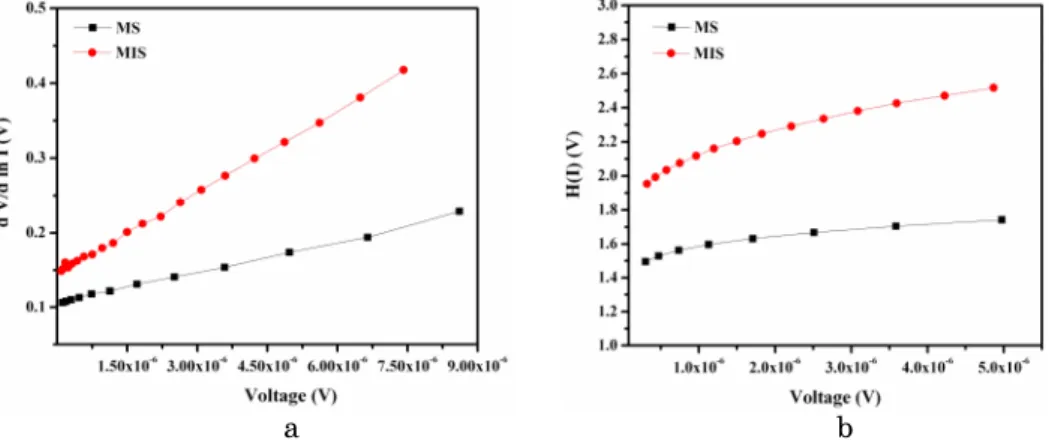
The values of series resistance Rs were estimated using the method developed by Cheung [8] at higher current range (over which the I-V characteristics is not linear). The Cheung’s functions are given as,
æ ö
= + ç ÷
è ø
(ln ) s
dV kT
IR
d I q (3)
æ ö
= - ç ÷
è ** 2ø
( ) nkT ln I
H I V
q AA T (4)
j
= +
( ) s b
H I IR n (5)
should give a straight line for the data of downward curvature region in the forward bias I-V characteristics. The term IRs is the current drop across the series resistance of Schottky diodes.
3.2 Determination of interface state density (Nss)
The interface state density for electrons or holes is always affected by the interfaces must not necessarily introduce energy levels in the band gap. At high forward bias voltages, the nonlinearity of the I-V characteristics of the MIS Schottky diode indicate the presence of continuum of interface states in equilibrium with the semiconductor [9]. The expression for the interface state density can be given as,
e e
d
é ù
= ê - - ú
ë û
1
( ) i( ( ) 1) s D
Nss V n V
q W (6)
where WD is the space charge region width, n(V) = V/(kT/q) ln(I/Is), es and ei are the permitivities of the semiconductor and the insulator layer (SiO2), respectively. In an n-type semiconductor, the energy of the interface states Ess with respect to the bottom of the conduction band at the surface of the semiconductor is given by,
j
- = ( - )
c ss b
E E q V (7)
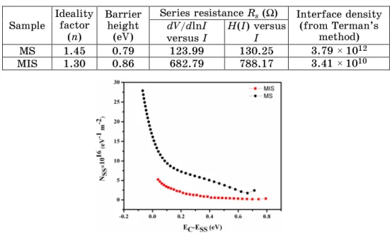
Equations (6)-(7), along with the I-V characteristics can be used for the determination of the interface state density as a function of interface states energy Ess with respect to the bottom of the conduction band. The resulting dependence of Nss was converted to a function of Ess using equation 7. Nss versus Ec - Ess is also shown in Fig. 3. Increase in effective barrier height jb of both the diodes forward bias is observed. This may be due to the increase in quasi-Fermi energy level of the majority carriers on the semiconductor side. This causes most of the electrons will be injected directly into the metal forming a thermionic emission current, while some of them are trapped by the interface states. This charge capture process results in an increase in effective barrier height thereby reducing the diode current [10, 11].
a b
Table 1 - Various parameters determined from I-V characteristics of MS and MIS n-GaN Schottky diodes
Sample
Ideality factor
(n)
Barrier height (eV)
Series resistance Rs (Ω) Interface density (from Terman’s
method) dV/dlnI
versus I
H(I) versus I
MS 1.45 0.79 123.99 130.25 3.79 × 10¹² MIS 1.30 0.86 682.79 788.17 3.41 × 10¹⁰
Fig. 3 - Interface state density distribution profiles as a function of Ec- Ess for MS and MIS diodes
The interface state density as determined by Terman’s method is found to be 3.79 ´ 1012 and 3.41 ´ 1010 cm- 2 eV - 1 for the MS and MIS Schottky diodes respectively [12]. From Fig. 3, it can be seen that an exponential increase in interface states density exists from mid gap towards the bottom of the conduction band. This rise is less significant for the MIS diode compared to that of the MS diode. At any specific energy, the interface state density of the MIS diode is less compared to that of the MS diode, which may be due to the fact that MIS diode has a thick oxide layer than that of the MS diode [10-11 and 13] because of the saturation of dangling bonds.
4. CONCLUSIONS
REFERENCES
1. S. Nakamura, M. Senoh, S. Nagahara, N. Iwasa, T. Yamada, T. Matsuahita, H. Kiyoki, Y. Sugimoto, Jpn. J. Appl. Phys.35, L74 (1996).
2. S. Nakamura, M. Senoh, S. Nagahara, N. Iwasa, T. Yamada, T. Matsuahita, H. Kiyoki, Y. Sugimoto, T. Kozaki, H. Umemeoto, M. Sano, K. Chocho, Appl. Phys. Lett. 72, 2014 (1998).
3. Y. Nakano, T. Jimbo, Appl. Phys. Lett.82, 218 (2003).
4. C. Bae, C. Krug, G. Lucovsky, J. Vac. Sci. Technol. A22(6),2379 (2004).
5. T.H. Tsai, J.R. Huang, K.W. Lin, W.C. Hsu, H.I. Chen, W.C. Liu, Sensor. Actuat. B-Chem.129, 292 (2008).
6. C.-Y. Hu, H. Nokubo, M. Okada, J.-P. Ao, Ohno, Jpn. J. Appl. Phys. 49, 04DF11
(2010).
7. S.M. Sze, Physics of Semiconductor Devices (Wiley Publishing: 1981). 8. S.K. Cheung, N.W. Cheung, Appl. Phys. Lett.49, 85 (1986).
9. H.C. Card, E.H. Rhoderick, J. Phys. D: Appl. Phys.4, 1589 (1971).
10.E.H. Rhoderick, R.H. Williams, Metal - Semiconductor Contacts (Clarendon Press: 1988).
11.A. Turut, M. Saglam, H. Efeoglu, N. Yalcin, M. Yildirim, B. Abay, Physica B 205, 41 (1995).