Three Phase High Power Quality
Two-Stage Boost Rectifier
P.NAMMALVAR*,
Senior Lecturer, Dept.of Electrical and Electronics Engineering, IFET college of Engineering,Villupuram.
Email: alvar1976@gmail.com.
S. ANNAPOORANI,
Assistant Professor, Dept. of Electrical and Electronics Engineering, Agni College of Technology, Chennai, Tamil Nadu, India.
Email: tannapoorani@gmail.com.
Abstract
Three-phase two-stage boost rectifier with sinusoidal input current are presented and a novel topology with two active power devices is proposed. These contain a capacitor for pumping action in DC circuit. This gives two-stage boost operation to obtain higher DC output voltage. The rectifier can be operated in the switch mode for pumping action and for forcing the input current to follow its sinusoidal reference independent of the working conditions. The results of the proposed rectifier are compared with those of the rectifier with a single active power device. The simulation result gives the better output DC voltage regulation under open loop condition. The simulated results prove that the proposed rectifier has the expected performance.
Keywords: Power Quality, Boost Rectifier, Total Harmonic Distortion
1. INTRODUCTION
To obtain higher DC output voltage, voltage-doubler rectifiers which are a half-bridge circuit or a diode pump circuit have been used [1–4]. The three phase circuit configuration of these rectifiers is simple, the AC input current has the distorted waveform. Use of a transformer allows multiple outputs to be obtained in the rectifier. Many circuits with the transformer have been reported [5–12]. The transformer is also used in isolated topologies and its design is important to reduce size, cost and losses.
For the purpose of the improved waveform in the input current by using new configuration of the rectifier without the transformer, the three-phase switch-mode rectifier with cascade connection of the diode bridge and the boost DC– DC converter has been shown [13]. However, the efficiency of the converter decreases rapidly at high duty cycle in the range of high DC output voltage. To maintain high efficiency in the wide operational range, a three-phase boost rectifier adding a capacitor for pumping action in DC circuit has been proposed by the authors [14]. This rectifier enables the DC output voltage to be regulated and the input current to be close to sinusoidal. However, the input current waveform is degraded as the output power increases.
In this paper, a novel three-phase two-stage boost rectifier without the transformer is proposed and a reduction in the input current distortion is studied. Additional capacitor in DC side gives two-stage boost operation by means of inductive and capacitive energy/transfer mechanisms under the high-frequency switching.
2. C
IRCUIT TOPOLOGIESFig. 1 gives the original topology of the three-phase two stage boost rectifier [14] which has been reported previously by the authors. This topology is based on the combination of a conventional three-phase boost rectifier and the pump circuit. The boost rectifier, which is first stage for the boost, comprises four diodes labelled D1–D4, an active power device IGBT labelled Q, the boost inductor L1 and the capacitor C1. The capacitor C2 for the pumping action, which functions as second stage for the boost, is connected in DC side. In the first stage, the energy is transferred from AC source to the capacitor C1.
The capacitor C2 for the pumping action, which functions as second stage for the boost, is connected in DC side. In the first stage, the energy is transferred from AC source to the capacitor C1. In the second stage, the energy stored in C1 is transferred to the capacitor C2. The pumping action of the capacitor C2 allows the output capacitor C3 to produce more than the sum of the peak input voltage and the capacitor C2 voltage, because C2 is connected in series to the input source.
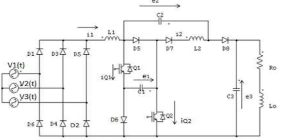
The inductor L2 is inserted to suppress the circulated current between the capacitors C1 and C2 in the on-state of Q. The diode D5 is inserted to prevent the capacitor C1 from being shorted when Q is turned on. The diode D6 prevents the current i1 from charging C1 through L1, C2 and L2 after the current i2 has reached to zero. The diode D7 prevents the capacitor C3 from discharging via C2 while Q is conducting. In this topology, the input current can almost be wave-shaped sinusoidally by employing a current-mode control. However, the rate of the increase in the input current during the conduction of Q depends on the supply voltage and the boost inductor L1. The low instantaneous supply voltage in the vicinity of a zero crossing cannot allow the actual current to follow the reference, so that the current waveform is distorted and is out of the sinusoidal wave near a zero crossing. The distortion in the input current becomes serious according to an increase of the load.
Fig.1 Three phase two stage boost rectifier with single switch
Fig. 2 shows the proposed three-phase two-stage boost rectifier for the purpose of the achievement of the sinusoidal input current without the distortion near the zero crossing of the supply. The diode bridge and the pump circuits also are employed for the construction of the topology. Comparing with Fig. 1, an active power device and a diode are added. The DC output voltage is more than twice the peak input voltage can be obtained.
In this topology, the voltage of the capacitor C1 can be used for the increase of the input current. Then the actual input current can go to the reference with faster response, even if the instantaneous supply voltage is low. Consequently, the distortion of the input current waveform in the vicinity of a zero crossing of the supply is reduced. The detail of the operation is described in the later section. The diodes D5 and D6 are inserted to prevent the capacitor C1 from being shorted when Q1 and Q2 are turned on.
3. SWITCHING AND CONTROL STRATEGIES
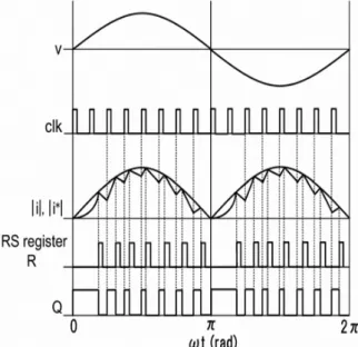
The basis of the boost rectifier with the current-mode control is as follows: the active power device is turned on at the beginning of the fixed interval, and it is turned off when the actual input current reaches the reference. The typical waveforms of the device signals and the input current are illustrated in Fig. 3 for the single-switch rectifier of Fig. 1, and in Fig. 4 for the proposed two-switch rectifier of Fig. 2. The device Q within the single-switch rectifier corresponds to Q1 within the two-switch rectifier. They are turned on by the clock pulse with the fixed frequency.
Fig -3 Device signals for single switch rectifier
The input current increases while the device conducts. The device is turned off by the reset signal when the instantaneous value of the input current is equal to that of the reference. The current decreases during the off-state of the device. In the two-switch rectifier, the active device Q2 is turned on to achieve the fast response with increasing input current. The conduction of this device allows the voltage of the capacitor C1 to contribute increasing the slope of the current. In the unity power factor condition, since the magnitude of the input current increases gradually during 0 ≤ωt ≤ π /2 and π ≤ωt ≤ 3π /2, the on-gate signals, which are identical with those of Q1, are applied to Q2 during these intervals.
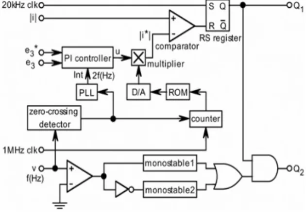
Fig. 5 illustrates the control block diagram for the proposed rectifier. This control circuit is also utilised for the single switch rectifier, and the output Q of the RS register is used for the on-gate signal of the devices Q. The feedback loop consists of the regulation of the DC output voltage and the generation of the sinusoidal input current. The control loop of the voltage mode compares the detected output voltage e3 against the command e3* and adjusts the input current to negate the voltage error. This is done by a proportional plus- integral (PI) controller. The computation of the PI algorithm is executed by a microcomputer in the test setup when the interrupt (INT) signal is provided by a phase locked loop at zero crossing every half-cycle of the supply. The output labelled u of the PI controller determines the amplitude of the current reference and it is discretely regulated with zero-order hold at every interruption. On the other hand, the control loop of the current mode contains the comparator and the RS register.
Fig -5 Control block diagram
The sensed instantaneous value i of the input current is converted into the absolute value , which is
one of the two inputs to the comparator. A read only memory (ROM) contains the digital data of a full-wave rectified sinusoidal signal with unity amplitude. A digital-to-analogue (D/A) converter changes the output of ROM into the continuous signal, which is kept in phase with the supply voltage. The reference [i*] of the input current is provided from the multiplier and it is given as a product of the signal u and the D/A converter output. The reference is the second input to the comparator. The switching timings of the two IGBTs labelled Q1 and Q2 are determined by the RS register with 20 kHz clock that is fixed as the switching frequency of IGBTs. The output Q of the RS register is set to the high level every clock cycle, and it is sent to the device Q1. The turn-on of this IGBT causes the actual input current [i] to increase. In[i*], the output of the comparator remains low and the IGBT is in the on-state. When the current [i] reaches[i*] the output of the comparator changes to the high level and so the output Q becomes low. This causes the IGBT to be turned off. The off-state of the IGBT allows the input current to decrease and it continues till the next clock pulse is provided to the RS register again.
As shown in Fig. 4, the on-gate signal with the duration π/2 is applied to the device Q2. This signal is generated by a mono stable. The mono stables 1 and 2 are triggered by the zero cross signal with the positive slope and the negative slope of the supply voltage, respectively. The outputs of two mono stables are sent to logic OR. This provides continuously the on-gate signal to Q2 during 0 ≤ωt ≤ π /2 and π ≤ωt ≤ 3π /2, The control scheme in this section can guarantee that the sinusoidal input current is maintained with a near unity power factor even if the load is varied.
4.
OPERATION OF CIRCUIT
the discontinuous i2. The single-switch rectifier has the same mode of the operation as the two-switch rectifier, except that the device Q2 conducts.
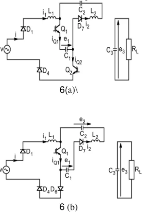
When the devices Q1 and Q2 are turned on, in the interval 0 ≤ωt ≤ π /2 , the circuit operation of mode 1 shown in Fig. 6a starts. In the interval π /2 ≤ωt ≤π , only Q1 is turned on and this mode of the operation is shown as mode 2 in Fig. 6b. In both modes, although the input current i1 increases and the energy is stored in the boost inductor L1, the response of the current differs between these modes.
6(a)\
6 (b)
Fig. 6:Modes of operation in on state of Q1
a) Mode 1 (Q2: on, i1≥ 0)
b) Mode 2 (Q2: off, i1≥ 0)
The current i1 in mode 1 flows through the following loop. v–D1–L1–Q1–C1–Q2–D4 and that in mode 2 flows through v–D1–L1–Q1–D6–D4
The increase of the input current in mode 1 is caused by the capacitor voltage e1 that is superimposed on the supply voltage, while the increasing current response in mode 2 depends upon the supply voltage only. The input current increases at a rate proportional to (|v |+ e1)/L1 and |v |/L1 in modes 1 and 2, respectively. In results, the input current increasing in mode 1 will have faster response than that in mode 2. The single-switch rectifier contains mode 2 only in the operation. The two-switch rectifier has the improved current waveform at the low instantaneous supply voltage, compared with that of the single-switch rectifier. On the other hand, in both modes, the current i2 that equals to iQ1 - iQ2 flow through the following loop
C1–D7 –L2–C2–Q1
and it increase at a rate proportional to (e1 - e2)/L2. The capacitor C1 is discharged and C2 is charged. As the energy stored in C1 is transferred to C2, the voltage e1 will decrease and e2 will increase slightly. In these modes, the diode D8 is reverse-biased and the load with C3 is isolated from the supply. The energy stored in the output capacitor C3 is supplied to the load and then the voltage across the capacitor C3 will decrease slightly.
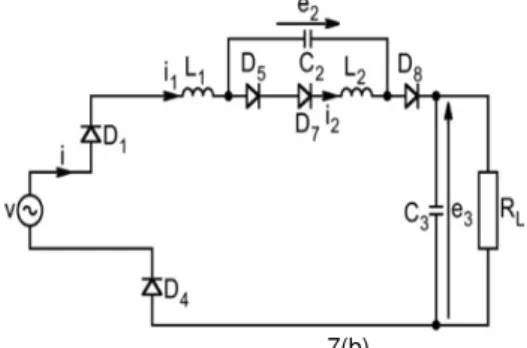
7(b)
Fig7 : Modes of operation with i2 = 0 in off states of Q1 and Q2
(a) Mode 3 (e1 + e2 <e3)
(b) Mode 4 (e1 + e2 >e3)
The device Q1 is turned off when the actual input current i in mode 1 or 2 reaches the reference. In mode 1, Q2 also is turned off simultaneously. Then mode 3 or 4 shown in Fig. 7 comes after mode 1 or 2, if the current i2 is not zero. The mode of the operation depends on the relationship of the capacitor voltages e1, e2 and e3. In the condition of e1 + e2 <e3, the diode D6 is in the on-state and D8 is reverse biased.
8(a)
8(b)
8(d)
Fig: 8 Modes of operation with i2 = 0 in off states of Q1 and Q2
(a) Mode 5 (e1 + e2 , e3, i1 >0) (b) Mode 6 (e1 + e2 . e3, i1 >0) (c) Mode 7 (e1 + e2 = e3, i1 > 0) (d ) Mode 8 (i1 = 0)
The current path of mode 3 shown in Fig. 7a is formed in the rectifier. The input current i1 flows through
v–D1–L1–D5–C1–D6–D4
and the capacitor C1 is charged. The current i2 circulates through
L2–C2–D5–D7
and it decreases with charging the capacitor C2. On the other hand, in the condition of e1 + e2 = e3, the diode D6 is blocked and D8 is on conducting. When i1 > i2, the current i1 flows through two paths, that is, C2 and D5–D7 – L2, as shown in Fig. 7b. The capacitor C2 is discharged and C3 is charged. If i1 < i2, the current i1 flows through D5–D7 –L2–D8, with charging C3. The circulated current of i2 - i1 flows in the loop L2–C2–D5–D7. The capacitor C2 is charged. In both modes, the input current i1 decreases.
When the current i2 is reduced to zero, in mode 3 or 4, the rectifier is in any mode of the operations shown in Fig. 8. Modes 5–7 of the operations have a non-zero current of i1. In mode 5 with the condition of e1 + e2 =e3, the diode D6 is in conducting and D8 is reverse biased. The current i1 flows through the following loop.
v–D1–L1–D5–C1–D6–D4
and the capacitor C1 is charged. The energy stored in the output capacitor C3 is supplied to the load. If e1 + e2 >e3, the diode D6 is blocked and D8 is in the on-state, as mode 6 shown in Fig. 8b. The current i1 flows into the load with the capacitor C3, through the capacitor C2. Then the capacitors C2 and C3 are discharged and charged, respectively. When e1 + e2 = e3, the rectifier is in mode 7 of the operation shown in Fig. 8c. In this mode, both the diodes D6 and D8 are in conducting. The current i1 flows through two paths
v–D1–L1–D5–C1–D6–D4
and
v–D1–L1–C2–D8–C3=RL–D4
5. SIMULATION
For the simulation of the operation in the rectifier shown in Fig. 2. In the experiments and the simulations, the operating conditions and the circuit constants are set as follows: V =50 V, f =60 Hz, L= 2.10 mH (R1= 0.108 Ω), L2 =13.8 mH (R2 = 4.40 Ω ), C1 =C2 =1000 µF, C3 = 2200 µF and RL= 62.5 Ω . The switching frequency is fs = 20 kHz corresponding to the clock frequency for the RS register.
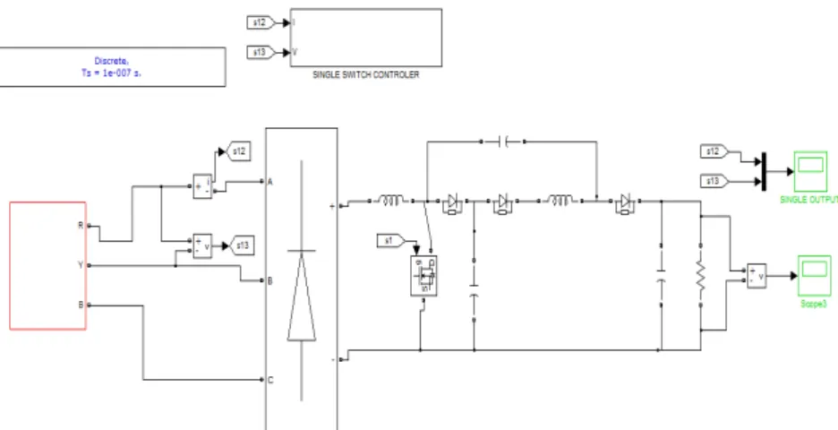
Fig 9:Simulation circuit of three phase two stage boost rectifier with single switch
Fig 10: Simulation output of three phase two stage boost rectifier with single switch
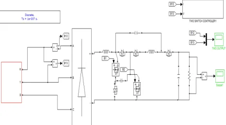
Fig 11 :Simulation circuit of three phase two stage boost rectifier with two switch
Fig 12: Simulation output of three phase two stage boost rectifier with two switch
Fig. 12 shows the simulation output current waveforms of the proposed two-switch rectifier with the same operating conditions as in Fig. 10. It is observed that the input current i can be sinusoidally wave-shaped without the distortion in the vicinity of a zero crossing of the supply and it is in phase with the supply voltage. The existence of mode 1 of the operation in the proposed rectifier contributes towards the achievement of the sinusoidal current.
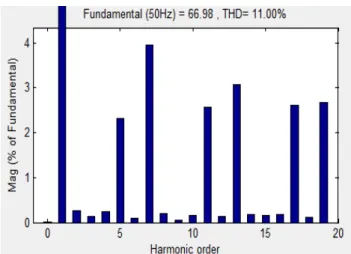
Fig 14:FFT analysis of three phase two stage boost rectifier with single switch
From the results of the FFT analyser in the input current, it has been seen that the THD is kept small enough over the range in all working conditions and it is shown in Fig14 and Fig 15.
Fig 15:FFT analysis of three phase two stage boost rectifier with two switch
6. CONCLUSION
A novel topology of the three-phase rectifier with two-stage boost operation has been presented, and the experimental and the simulated results have been shown in this paper. The proposed rectifier has an additional active power device as against the previous rectifier. The switching operation of this device contributes to the achievement of the input current waveform. The experimental results under steady state condition prove that the input current of the proposed rectifier becomes more sinusoidal in the waveform and contains the reduced harmonics, compared with that of the previous one. From the results of the FFT analyser in the input current, it has been seen that the THD is kept small enough over the range of the demonstrated working conditions. The simulated waveforms, which are obtained by using the state-space method, are in good agreement with the experimental ones. Consequently, it is considered that the proposed rectifier is suitable for AC–DC conversion equipment with the booster capability and the high-quality input current although the use of many devices leads to slight decrease in the efficiency.
7. REFERENCES
[1] BOYS J.T., GREEN A.W.: ‘Current-forced single-phase reversible rectifier’, IEE Proc., Electr. Power Appl., 1989, 136, (5), pp. 205– 211.
[2] SALMON J.C.: ‘Circuit topologies for single-phase voltage doubler boost rectifiers’, IEEE Trans. Power Electron., 1993, 8, (4), pp. 521–529 .
[3] MAZDA F.F.: ‘Power electronics handbook’ (Butterworths, 1990).
[4] SINGH B., SINGH B.N., CHANDRA A., AL-HADDAD K., PANDEY A., KOTHARI D.P.: ‘A review of single-phase improved power quality AC–DC converters’, IEEE Trans. Ind. Electr., 2003, 50, (5), pp. 962–981.
[6] DANIELE M., JAIN P.K., JOOS G.: ‘A single-stage power-factor corrected AC/DC converter’, IEEE Trans. Power Electron., 1999, 14, (6), pp. 1046–1053.
[7] CHOW M.H.L., LEE Y.S., TSE C.K.: ‘Single-stage single-switch isolated PFC regulator with unity power factor, fast transient response, and low-voltage stress’, IEEE Trans.Power Electron., 2000, 15, (1), pp. 156–163.
[8] WEI H., BATARSEH I., ZHU G., KORNETZKY P.: ‘A single-switch ac– dc converter with power factor correction’, IEEE Trans. Power Electron., 2000, 15, (3), pp. 421–430.
[9] QIAO C., SMEDLEY K.M.: ‘A topology survey of single-stagepower factor corrector with a boost type input- currentshaper’, IEEE Trans. Power Electron., 2001, 16, (3), pp. 360–368 .
[10] LU D.D.C., CHENG D.K.W., LEE Y.S.: ‘Single-stage AC–DC power-factor-corrected voltage regulator with reduced intermediate bus voltage stress’, IEE Proc. – Electr. Power Appl., 2003, 150, (5), pp. 506–514.
[11] LIN J.L., CHANG M.Z., YANG S.P.: ‘Synthesis and analysis for a novel single-stage isolated high power factor correction converter’, IEEE Trans. Circuit Syst. I, 2005, 52, (9), pp. 1928–1939.
[12] LU D.D.C., IU H.H.C., PJEVALICA V.: ‘A single-stage ac/dc converter with high power factor, regulated bus voltage, and output voltage’, IEEE Trans. Power Electron., 2008, 23, (1), pp. 2274–2286.
[13] TAKAHASHI I., IKESHITA W.: ‘Improvement of input current waveform of a single-phase rectifier circuit’, Trans. IEE Jpn, 1985, 105-B, (2), p. 82.