Development and characterization of
Undoped Silicon Glass (USG) using
chemical vapour deposition
Jagadeesha T a, Louis Kimb, Joseph Gonsalvisc, Thammaiah Gowdad
a
Department of Mechanical Engineering,National Institute of Technology,Calicut,673 601 , India
b
ThinFilm Division, Chartered Semiconductor Manufacturing, Woodlands, Singpaore
c
Department of Mechanical Engineering, SJEC, Vamanjoor, Mangalore 575 028, India
dDepartment of Industrial &Production Engineering, AIT,Chikmagalur 577 102, India
Abstract: Sub atmospheric chemical vapour deposition (SACVD) is a widely used technique in semiconductor integrated circuit (IC) manufacturing, especially to form inter-metal silicon (IMD) dioxide thin films. It was designed for commercially available tools in order to satisfy the gap filling requirements necessary for 0.18 and 0.15 lm technology ICs, but it has been successfully extended also for 0.13 lm technological node and over. SACVD technique has a potential impact on device electrical characteristics and metallurgy compatibility, according to process conditions, such as mass flow rate of TEOS, Gas flows, RF power. Present work focuses on development and characterisation of undoped silicate glass that can be used for Flash memory and Logic devices. It is shown that new process yield deposition rate improvement of 51% and throughput improvement of 13%.. Qualitative yield comparison and wafer map to map comparison work is also presented for various technology nodes. Device parameters comparison with the standard process is also included in the present work.
Keywords: BPSG, PSG, Low pressure BPSG, SACVD
1. INTRODUCTION
Dielectric layers are necessary in the circuit design to isolate the metal or polysilicon lines and prevent device shorting. Given the demand for decreased circuit dimensions, dielectrics deposited at low temperatures and with acceptable gapfill are becoming increasingly important [1–9]. The low deposition temperatures necessary to prevent overheating of the underlying structures and gapfill abilities to prevent unwanted voids are making plasma deposition of dielectric films an increasingly critical part of microelectronic circuit manufacturing [10]. The necessity to drive to smaller circuit dimensions is requiring the development of thin dielectric
Dielectric levels that can act as contamination barriers as well as have the ability to be deposited within narrow features without leaving voids. This requirement necessitates the use of multi-layered dielectric deposition in which the first layer is to have excellent film quality and gapfill properties and subsequent layers to be used primarily topography control and contamination barriers. The same unique film properties that make those films invaluable can lead to problems related to the stability of the two films at the interface. An example of this can be noted at the pre-metal dielectric (PMD) level used in semiconductor manufacturing. The main purpose of the PMD layer is to isolate the transistor region from the effects of metal interconnect layer processing. The first isolation role the PMD layer plays is to isolate the transistor area from electrical signals and plasma effects from the metal processing. Secondly, the PMD layer acts as a physical barrier to prevent mobile ions from metal and photolithography processing
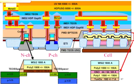
Figure 1: Device application of USG layer
2. EXPERIMENTAL DETAILS.
Figure 2: Producer Tool used for deposition process
This work provides a new and improved process for filling small-width, high-aspect ratio gaps with a SACVD layer. The present invention deposits a low pressure SACVD layer over a small-width, high-aspect ratio gap that requires filling with a dielectric material. The relation between the mass flow rate of TEOS versus deposition rate was first established using the producer tool equipped with PLIS (Precision Liquid Injection System).The effect of the other parameters were also studied and found that mass flow rate of TEOS had greater influence on the deposition rate and Fig. 3 shows the other parameters considered and Fig. 4 shows the effect of varying the pressure of process.
Figure 3: Process parameters studied to optimize the USG parameters.
Effect of TEOS flow on SA USG Dep Rate (A/m in)
0 200 400 600 800 1000
900 1000 1150 1250 1300 1350
TEOS flow rate (m gm )
D
e
po
s
iti
on
R
a
te
(
A
/m
in
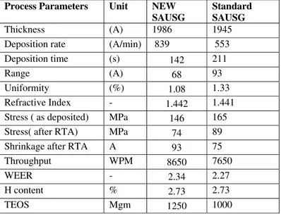
the deposition rate, deposition temperature , post annealing cycle, dopant concentration, film porosity, and water content. Hence, the processing of silicon dioxide should be carefully controlled. Table 1 shows the comparison between 1250 mgm and 1000 mgm TEOS processes. Process parameters indicated in the Table 1 are the average values of measurement taken over 220 wafers and for various technology nodes ranging from 0.13 micron to 0.1 micron devices. It is clear from the experimental results that 1250 mgm process gives lowest processing time. Range difference up to 15 Å is observed between chamber 1 and chamber 2. This difference is due to heater and other hardware settings. The range can be further reduced by fine tuning of hardware. Wet etch rate (WER) measurements have been performed with a time/stop technique in a 7:1 H2O:HF solution,
NH4F buffered, at temperature T = 20 ± 0.50 C . The experimental error was estimated in ±10%.To attain an
absolute comparison, the etch rate of the HDPCVD silicon dioxide samples was divided by that obtained from reference thermal oxide (wet etch rate ratio, hereafter _WERR_): obviously WERR has always values >1. For Si–OH bond detection, room temperature IR absorption measurements were performed in the wave number range from 3300 to 4000 cm_1 using a FTIR spectrometer Nicolet Eco1000. model. Thirty two scans were performed for every sample under analysis and instrumental resolution was 4 cm-1.
Process Parameters Unit NEW SAUSG
Standard SAUSG
Thickness (A) 1986 1945 Deposition rate (A/min) 839 553 Deposition time (s) 142 211 Range (A) 68 93 Uniformity (%) 1.08 1.33 Refractive Index - 1.442 1.441 Stress ( as deposited) MPa 146 165 Stress( after RTA) MPa 74 89 Shrinkage after RTA A 93 75 Throughput WPM 8650 7650 WEER - 2.34 2.27 H content % 2.73 2.73 TEOS Mgm 1250 1000
Table 1: Comparison of 1250 mgm and 1000 mgm TEOS Processes
3.2 Thicknes Range Improvement and TEPO usage reduction
Table 2: Comparison of 100 Torr and 200 Torr processes in terms of performance parameters.
3.3 Yield results
For use in ULSI devices the reliability of silicon dioxide is important. Hence , the time for failure and charge to breakdown under constant voltage or constant current stress are analysed to determine the oxide quality. The stress in silicon dioxide can change the film quality. Table 3 and Table 4 shows the yield results of the 1200 mgm and 1000 mgm processes. Experiments were conducted on different devices using different technology nodes. Yield results are quite comparable and the 1200 mgm processes give better yield , which is desirable from the productivity point of view.It can also be observed that the 1200 mgm processes are technology node and device independent. Table 5 shows the ANOVA results of yield comparsion for both 1200 mgm and 1000 mgm process. It can be observed from the Table 5 that yield results are spread widely for 1000 mgm process compared to 1200 mgm process. Also yield values are high for 1200 mgm process.
Table 3: Yield results of 1200 mgm process for different technology nodes and devices
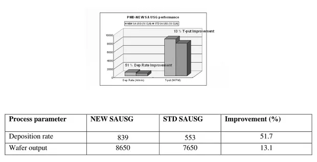
Process parameter NEW SAUSG STD SAUSG Improvement (%)
Deposition rate 839 553 51.7 Wafer output 8650 7650 13.1
Lot ID Technology
Node Device CP1(%) CP2(%)
S1 1 D1 87 87.6
S2 1 D2 87.6 84.3
S3 1 D3 86.6 85.5
S4 1 D4 75.5 75.6
S5 2 D5 84.3 83.3
S6 2 D6 80.32 78.91
Table 4: Yield results of 1000 mgm process for different technology nodes & devices
Table 5: ANOVA results of 1000 mgm process for different technology nodes & devices
3.4 Gap filling capability
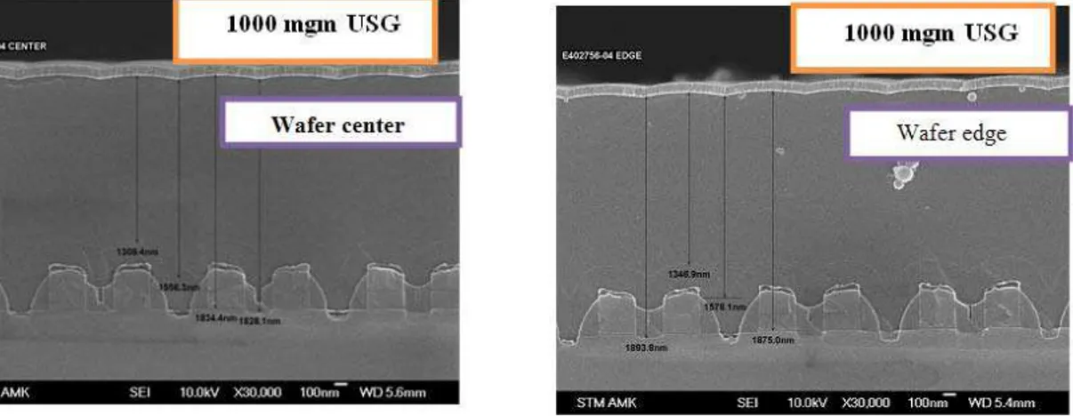
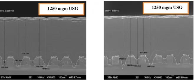
Figure 5 and Figure 6 shows step coverage for 1000 mgm and 1250 mgm processes. Both processes give completely uniform or conformed step coverage. The film thickness along the walls and at the bottom of step are constant. As the reactants or reactive intermediates adsorb on the surface and then rapidly migrate along the surface before reaction, the resulting films will have a uniform surface concentration on the substrate and constant thickness. It is important to avoid cusp formation, it will be unfavorable for subsequent metal deposition.
Figure 5: Gap filling capability of 1000 mgm USG layer (both at wafer edge and center)
Figure 6: Gap filling capability of 1250 mgm USG layer (both at wafer edge and center)
4. CONCLUSIONS
In this paper, a new and improved process for filling small-width, high-aspect ratio gaps with a undoped silicate glass (USG) layer using SACVD has been presented. The present invention deposits high flow USG layer over a small-width, high-aspect ratio gap that requires filling with a dielectric material. It is shown that by changing the mass flow rate from standard 1000 mgm to 1250 mgm , deposition rate can be increased. Range improvement of 15.2 % is seen for 1250 mgm process compared to 1000 mgm process. Cost per wafer using 1200 mgm is less compared to 1000 mgm process due to high deposition rate and low TEPO usage. Yield results and gap filling capabilities of both processes are comparable. The feasibility of the new fabrication process has been demonstrated with production wafers and found to be technology node and device independent.
REFERENCES
[1] Tsuyoshi Hata, Hiroshi Nakayama, An organic catalytic CVD: Principle, apparatus and application, Journal of Thin Solid Films, Volume 516, 2008, Pages 558-563.
[2] A. Morales, J.Barreto, C. Dominguez, M. Riera, Comparative study between silicon rich oxide films obtained by LPCVD and PECVD, Journal of Physica E. Volume 38, 2007, Pages 54-58.
[3] Ch. Voulgaris, A. Panou, E. Amanatides, D. Mataras, RF power effect on TEOS/O2 PECVD of silicon oxide thin films, Journal of Surface coating and technology, Volume 200, March 2005, Pages 351-354.
[4] G. Gulleri, C. Carpanese, C. Cascarano, D. Lodi, Deposition temperature determination of HDPCVD silicon dioxide films, Journal of Microelectronics Engineering, Volume 82, 2005, Pages 236-241
[5] K. Schade, F. Stahr, S. Rohlecke, O. Steinke, R.H. Richer, Very high frequency plasma CVD of Silicon oxide, Journal of Surface coating and technology, Volume 200, March 2005, Pages 364-367.
[6] Haruhisa Kinoshita, Naoki Otaka, Influence of plasma heating of wafer substrates on SiO2 deposition rate in TEOS/O2 high density plasma CVD system, Journal of Surface Engineering, Surface Instrumentation and Vacuum Technology, Volume 74, 2004, Pages 99-104.
[7] M.F.A.M. Van Hest, B. Mitu, D.C. Schram, M.C.M. Van de sanden, Deposition of orthanosilicon thin films using a remote thermal plasma, Journal of Thin Solid Films, Volume 449, 2004, Pages 52-62.
[8] S. B. Bang, T.H. Chung, Y. Kim, Plasma enhanced chemical vapour deposition of silicon oxide films using TMOS/O2 gas and plasma diagnostics, Journal of Thin Solid Films, Volume 444, 2003, Pages 125-131.
[9] K. Saito, Y. Uchiyama, K. Abe, Preparation of SiO2 thin films using the cat-CVD method, Journal of Thin Solid Films, Volume 430, 2003, Pages 287-291.
[10] D.M. Kremer, R.W. Davis, E.F. Moore, S.H. Ehrman, A numerical investigation of the effects of gas phase particle formation on silicon film deposition from silane, Journal of Crystal Growth, Volume 247, 2003, Pages 333-356.
[11] Chung Yi, Hyo Uk Kim, Shi Woo Rhee, Improvement of the SiO2/Si interface characteristics by two step deposition with intermediate plasma treatment using N2/He or O2/ He gas, Journal of Thin Solid Films, Volume 408, 2002, Pages 252-259.