Article
Printed in Brazil - ©2014 Sociedade Brasileira de Química0103 - 5053 $6.00+0.00
A
*e-mail: [email protected]
Tungsten Oxide Thin Films Grown by Thermal Evaporation with
High Resistance to Leaching
Diogo S. Corrêa,a Julia C. O. Pazinato,b Maurício A. de Freitas,b Lucio S. Dorneles,c
Claudio Radtkeb and Irene T. S. Garcia*,b
aCentro de Ciências Químicas, Farmacêuticas e de Alimentos, Universidade Federal de Pelotas,
Campus Capão do Leão, s/n, 96010-900 Pelotas-RS, Brazil
bInstituto de Química, Universidade Federal do Rio Grande do Sul,
Av. Bento Gonçalves, 9500, 91501-970 Porto Alegre-RS, Brazil
cCentro de Ciências Naturais e Exatas, Universidade Federal de Santa Maria,
Campus Camobi, s/n, 97105-900 Santa Maria-RS, Brazil
Óxidos de tungstênio apresentam diferentes estequiometrias, estruturas cristalinas e morfologias. Estas características são importantes principalmente quando se deseja utilizá-los como fotocatalisadores. Neste trabalho foram obtidos filmes finos de óxido de tungstênio por evaporação térmica sobre substratos de silício (100) recobertos com ouro, aquecidos a 350 e 600 °C. A estequiometria dos filmes formados, morfologia, estrutura cristalina e resistência à lixiviação foram caracterizadas por espectroscopia de fotoelétrons de raios X, espectroscopia micro-Raman, microscopias eletrônicas de varredura e transmissão, difratometria de raios X, espectrometria de retroespalhamento Rutherford e reação nuclear ressonante O16(α,α´)O16. Os filmes apresentam estrutura nanométrica, cuja forma torna-se bem definida com o aumento da temperatura. O sistema apresenta-se na forma de WO3.1 e cristaliza principalmente na fase hexagonal, sendo obtidas também estruturas de óxido de tungstênio hidratadas. Os filmes obtidos através de evaporação térmica apresentam resistência à lixiviação em ambiente aquoso e excelente atividade fotocatalítica, que foi testada na degradação do corante alaranjado de metila.
Tungsten oxides show different stoichiometries, crystal lattices and morphologies. These characteristics are important mainly when they are used as photocatalysts. In this work tungsten oxide thin films were obtained by thermal evaporation on (100) silicon substrates covered with gold and heated at 350 and 600 °C, with different deposition times. The stoichiometry of the films, morphology, crystal structure and resistance to leaching were characterized through X-ray photoelectron spectroscopy, micro-Raman spectroscopy, scanning and transmission electron microscopy, X-ray diffractometry, Rutherford backscattering spectrometry and O16(α,α´)O16 resonant nuclear reaction. Films obtained at higher temperatures show well-defined spherical nanometric structure; they are composed of WO3.1 and the presence of hydrated tungsten oxide was also observed. The major crystal structure observed is the hexagonal. Thin films obtained through thermal evaporation present resistance to leaching in aqueous media and excellent performance as photocatalysts, evaluated through the degradation of the methyl orange dye.
Keywords: tungsten oxide, thermal evaporation, leaching resistance, photocatalysis
Introduction
The class of transition metal oxides drives attention of many researchers, particularly when the preparation of photocatalyst devices is concerned. In the last years,
tungsten oxide has been highlighted due to its band gap, smaller than that of titanium oxide, which therefore allows the absorption of radiation by the tungsten oxide to occur
in the visible region of the electromagnetic spectrum.1 The
capacity to achieve different oxidation states (–II to +VI)2,3
studied hexagonal (h-) and monoclinic (m-) tungsten oxide in oxidized and reduced forms and found that the oxidized species present improved photocatalytic performance compared to the reduced form.
Crystal size, surface area, lattice defects and morphology affect the electrochemical properties of this material and are
important aspects in the development of technologies7,8 with
applications primarily in photocatalysis,9 gas sensing10,11
and electrochromic devices.12
Many photocatalytic processes use metal oxide powders, but getting those supported facilitates subsequent removal from the reaction medium. Techniques for obtaining tungsten oxide films have an important role, mostly in structuring and modifying stoichiometry. These techniques may include chemical processes, such as
structuring methods in a liquid medium (sol-gel)13 and
chemical vapor deposition,14-16 or physical processes, such
as sputtering,17 electron beam and thermal evaporation.18,19
A simple method that allows obtaining different structuring modes is based on the deposition by thermal
evaporation.20,21 This technique consists in heating the
material which is vaporized and transported to the substrate. The appropriate handling of experimental parameters allows different chemical characteristics to be obtained. The deposition temperature can influence the crystal size and morphology, two factors that promote change in crystal lattice at lower temperatures than those reported
in bulk form22 and can also promote the formation of
non-stoichiometric tungsten oxides (WOx, x = 2 to 2.5).23
Hieu et al.10 synthesized WO
3 nanowires through thermal
evaporation using WO3 powder on W substrates and
observed that, at higher temperatures (1050 °C), porous structures were generated.
Pressure changes affect the free path of the vaporized
material and morphology of the produced films. Liu et al.24
reported that the increase of efficiency in the growth of zinc oxide nanowires, nanobelts and nanocombs was related to
the decrease of pressure. Thermal evaporation of WO3 at
1.3 × 10⁻¹ Pa and 1000 °C on Si(100) substrate produced
monoclinic single crystals as nanorods with nanometric
diameters and lengths up to a few tens of micrometers.11
This method can be also used for obtaining WO3/Au/WO3
and WO3/Ag/WO3 multilayer coatings deposited at
5 × 10⁻⁴ Pa. These coatings present high transmission in the visible region of the spectrum, together with simultaneous
suppression of the near-infrared transmission.25,26
Nanowires composed of W18O49 can be prepared through
thermal evaporation at 2.7 × 10⁻¹ Pa on Au/Co/SiO
2/Si
substrates heated at 650 °C.27
The atmosphere of the deposition chamber is an important aspect to be observed when different
stoichiometries are desired. Gases such as H2 and N228 are
commonly employed to promote a reducing atmosphere
that in turn gives substoichiometric oxides. Air and O213
permit the achievement of oxides with the metal atom at its higher oxidation number. The substrate characteristics can also affect the epitaxy of the formed films. The growth of ZnO single crystals on silicon substrates, via thermal evaporation, shows preferential growth in the direction of
the silicon c-axis, allowing the formation of nanostructures
perpendicular to the substrate.29 Nano-polycrystalline
WO3 100-200 nm films are obtained on indium tin oxide
(ITO)/glass substrates,30 while cubic high density WO
3 was
obtained on ITO-coated glass substrates.31
In this work we obtained WO3 thin films by thermal
evaporation under reduced oxygen pressure. The films were obtained on (100) silicon substrates coated with a thin gold layer. We analyzed the effect of substrate temperature
(TS) on the composition of the films, structuring mode and
crystalline lattice. Resistance to leaching, an important aspect to be considered when planning to use these films as catalysts in aqueous media, was also evaluated. We also tested these films in the degradation of a very stable anionic dye, methyl orange (4-dimethylaminoazobenzene-4’-sulfonic acid sodium salt), used in the textile, printing,
paper manufacturing and pharmaceutical industries.32
Experimental
Materials
The films were obtained from WO3 in powder form,
produced by Sigma-Aldrich (99.5% of purity). The substrate was silicon (100) covered with a gold layer with an average thickness of 26 ± 8 nm (Au/Si). The substrates were cleaned through immersion in acetone during 15 min, immersion in water during 10 min and drying for 2 h at 110 °C.
Preparation of the films
Films were obtained in a horizontal furnace provided with a ceramic tubular chamber. Temperature was previously calibrated as a function of distance to the center of the furnace. The substrates were disposed horizontally in places with temperatures of 350 and 600 °C and oxygen was admitted into the chamber. During the deposition, the pressure inside the chamber was maintained at 15 mtorr. The tungsten oxide powder was heated from 25 °C up to
1100 °C with a heating rate of 20 °C min-1 and the higher
20 °Cmin-1 cooling rate. At the end of the cooling process, the chamber was driven to the atmospheric pressure.
Characterization
The oxide stoichiometry was obtained by X-ray photoelectron spectroscopy (XPS), carried out with an
Omicron EA 125 analyzer using Mg-Kα radiation with
energy of 1253.6 eV. The chamber was operated at 10-6 mtorr
and 25 °C. The film surface was cleaned by sputtering with an argon beam (1 keV). The zones of specific energy for W 4f and O 1s were analyzed in high resolution.
The micro-Raman spectra were obtained by incidence
of a He-Ne laser of 10 mW and λ = 632.9 nm, with normal
incidence as related to the sample. A Jobin-Yvon HR 320 monochromator was used for the collection of the scattered radiation and an EGG Princeton Application Research 1530-C-1024S device was employed as a cryogenic detector.
Scanning electron microscopy (SEM) was carried out on a JEOL JSM 6060 microscope with 20 kV voltage. The high-resolution transmission electron micrographs (HRTEM) were obtained with a JEOL JEM 2010 microscope with 200 kV voltage. The samples were prepared in cross section mode, allowing visualization of the film profile.
Powder X-ray diffractometric analysis (XRD) was carried out on a Bruker D8 Advance diffractometer using
θ-2θ geometry and equipped with a Cu anode (Cu-Kα,
λ = 1.541 Å) and a LinksEye detector. Values of 2θ ranged
from 10 to 50° and the scan rate employed was of 0.5° min-1.
The obtained data were compared with reference data available from the Joint Committee on Powder Diffraction Standards (JCPDS) library.
Leaching resistance test
Tungsten oxide is not soluble in acidic solution; however, to characterize the resistance of these oxide films to leaching, it is important to prevent them from going into aqueous medium during their use. A film not resistant to leaching can have its use as photocatalyst overshadowed by water contamination with the oxide and will require an extra step of filtration. The tungsten oxide films supported on Au/Si substrates, with thickness previously evaluated through Rutherford backscattering spectrometry, were immersed in pH 6.0 aqueous solution (adjusted with
a solution of HCl 0.1 mol L-1) during 30 min at room
temperature and dried at 110 °C during 1 h. After this leaching test, a new determination of the film thickness took place. The conditions of the test were defined based
on the conditions reported in the literature for degradation
of some azo and aromatic compounds.33,34
Rutherford backscattering spectrometric analysis (RBS) was performed on a TANDEM High Voltage Engineering
Europe particle accelerator of 3 MV, using a He+ beam
with 800 keV. The incoming beam was configured with incidence angle of 0° and the Si/Li solid detector was positioned at 15° with respect to the normal to the film surface.
The oxygen profiles under the film surface were
obtained through O16(α,α')O16 resonant nuclear reaction
analysis (NRA), using an α particle beam with energies
of 3047, 3053 and 3077 keV to determine the oxygen content in the depths of 8, 30 and 120 nm, respectively. The
incidence angle of the α particles was 0° and the detector
was positioned at 15° with respect to the normal of the film. This analysis is important to characterize possible variations in the amount of oxygen up to 120 nm below the film surface.
Photocatalytic activity
A PHILIPS PL-S 11 W lamp (250 nm) was used as the radiation source to estimate the photocatalytic activity
of WO3 films. These tests were carried out by monitoring
the degradation of the methyl orange dye (MO). Two
systems composed of 15 mg L-1 MO and 3% v/v H
2O2
were prepared. Prior to illumination, 2.5 cm2 area films
were immersed in one dye/H2O2 system and kept there for
30 min to reach the adsorption-desorption equilibrium. The photocatalytic reaction was initiated by exposing both systems, with and without film, to radiation at 25 °C. Aliquots (3.5 mL) of the reaction mixture were analyzed by UV-Vis spectrophotometry from 350 to 600 nm after each reaction period of 60 s. The intensity of the high
molar absorptivity peak at λ = 469 nm in the spectrum of
the model dye was used as the reference to measure the residual dye concentration as a function of time.
Results and Discussion
Composition
The XPS spectra for the WOx/AuSi films show the
presence of two peaks attributed to tungsten (Figure 1a) and to oxygen (Figure 1b). Two peaks at 35.55 and 37.68 eV
are attributed to the 4f7/2 and 4f5/2 tungsten electrons,
respectively. The deconvolution of this spectrum, shown in Table 1, indicates the presence of tungsten oxidized
forms, WVI (77.5%) and WV (22.5%).35 Figure 1b shows
of this spectrum reveals peaks with a binding energy close
to that observed by Szilágyi et al.6 (see Table 1).
The O 1s (1) peak is related to the O2– speciefrom the
tungsten oxide lattice and the O 1s (2) and O 1s (3) peaks
are associated with OH– and H
2O species that result from
surface interaction of the metal oxide with hydrogen and
water.6 The presence of WVI (WO
3), WV (W2O5) and oxide
associated with H2O are confirmed by Raman analysis.
The stoichiometric ratio, calculated through the O 1s (1) oxygen and W 4f normalized areas, is 3.1.
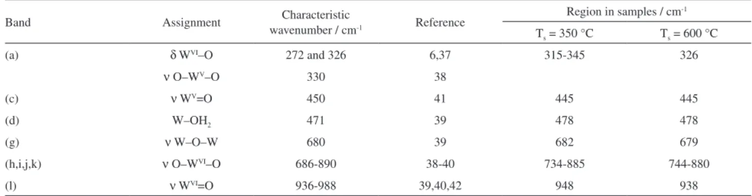
Raman spectra, Figure 2, provide information about the chemical composition and crystal phase of the material. The attributions of the main bands are presented in Table 2.
Because the thin films were obtained on Au/Si, a Raman spectrum of the substrate was added to Figure 2 in order to
identify the contribution originated from gold (298 cm-1)36
and silicon (520 cm-1 and 948-980 cm-1).37 Films obtained
in this work, at 350 and 600 °C, present bands at 639 (f), 683 (g) and 820 cm-1 (j) which, according to Szilagyi et al.,6
can be related to h-WO3. Boulova and Lucazeauw22
characterized monoclinic, triclinic and tetragonal WO3
phases by Raman spectroscopy, but these phases could not be obtained in the present work.
Chemical bonds to WVI are stronger than to WV; so,
vibrations of the fully oxidized tungsten are expected to
occur at energies higher than those of WV.38 Additional
broad bands at 330 (a) and 445 cm-1 (c) are therefore
related to vibrations of the O–WV–O and WV=O bonds,
respectively. The signal at 445 cm-1 can be attributed to
the presence of W–OH2 bonds,39 which is confirmed by the
shoulder at 647 cm-1 (f) originated from ν(O–W) in hydrate
oxide.40 The Raman signals at 947 and 939 cm-1 of samples
obtained at 350 and 600 °C, respectively, are attributed to
WVI=O bonds (l).37 These results corroborate XPS data
and permit to conclude that, in both temperatures, films
are mainly composed of WVI but also present WV oxide as
a hydrated species.
Structural characterization
SEM micrographs (Figure 3) show that the substrate temperature is a determining factor in the development
of grain morphology. Films deposited at Ts = 350 °C
(Figure 3a) show very irregular structures which suggest that they are growing in a coalescence process. Films
deposited at Ts = 600 °C (Figure 3b) present grains with
regular spherical shape. The migration process of the grains
on film surface can be followed through a continuous WO3
path that ends in a WO3 grain (see white arrow in Figure 3b).
Table 1. Binding energies obtained from fitting the XPS spectra of Figure 1
Photoelectron region Binding energy / eV Chemical species present in film
W 4f7/2 (1) 34.9 WV
W 4f7/2(2) 35.5 WVI
W 4f5/2 (3) 36.1 WV
W 4f5/2 (4) 37.6 WVI
O 1s (1) 530.2 O2–
O 1s (2) 532.1 OH–
O 1s (3) 532.6 H2O
Figure 1. High-resolution XPS spectra for the sample obtained at Ts = 350 °C for 90 min in the (a) W 4f and (b) O 1s region.
The development of grains consists of a nucleation process, surface-diffusion controlled growth of the nuclei, and the formation of a continuous film. Both samples
present a continuous WO3 layer and, on this layer, WO3
grains. Micro-Raman analyses taken with the laser beam focused on the continuous part of the films (Figure 3c) and on the grains (Figure 3d) corroborate this observation, which can be associated with the structuring model of
Stranski-Krastanov.20
The size distribution analyzed by SEM (Figure 4) shows that both samples present a wide grain size distribution, which is slightly narrower for samples obtained at Ts = 600 °C.
TEM analysis corroborates the proposed growth model, in which it is possible to identify, through cross section micrography (Figure 5a), the difference between the film thickness and the substrates, silicon and gold. In HRTEM (Figure 5b), it is possible to observe the atomic plane disposition, in which the growth occurs with preferential
direction (100). The interplanar distance, measured through
the use of imageJ® software, has an average value of 3.3 Å.
The X-ray diffractograms shown in Figure 6 indicate presence of both amorphous and crystalline material. The main crystalline phase, identified by the three main peaks
at 2θ = 28.1, 13.9 and 36.6°, is hexagonal tungsten oxide
Table 2. Attributions of the Raman spectra
Band Assignment Characteristic
wavenumber / cm-1 Reference
Region in samples / cm-1
Ts = 350 °C Ts = 600 °C
(a) δ WVI–O 272 and 326 6,37 315-345 326
ν O–WV–O 330 38
(c) ν WV=O 450 41 445 445
(d) W–OH2 471 39 478 478
(g) ν W–O–W 680 39 682 679
(h,i,j,k) ν O–WVI–O 686-890 38-40 734-885 744-880
(l) ν WVI=O 936-988 39,40,42 948 938
Ts: substrate temperature.
Figure 3. Micrographs (20 kV) of the WO3/AuSi films obtained (90 min
deposition) obtained at 350 °C (a) and 600 °C (b). White arrows show the possible formation path for a WO3 grain. Micro-Raman analyses were performed with a laser beam focused on the continuous part of the film (c) and on the grain (d). Attribution of these spectra can be seen in Table 2.
Figure 4. Histogram of size distribution for WO3 films obtained with a
deposition time of 90 min.
Figure 5. TEM micrograph (accelerating voltage = 200 kV) of a WO3/
AuSi film obtained at Ts = 350 °C and revealing (a) WO3 deposition over a
(h-WO3, JCPDS # 01-075-2187). The crystallite size could be estimated from the Scherrer equation:
(1)
where d is the crystal diameter, K = 0.9, λ(Cu Kα) = 1.5405 Å,
θ is the Bragg diffraction angle and β the full width at half maximum (in radians) of the Bragg peaks.
The tungsten oxide crystal size calculated from [200]
planes (at 2θ = 28.1°) is about 33 nm for the sample
obtained at Ts = 350 °C and 59 nm for that obtained at
Ts = 600 °C. There are two peaks at 2θ = 18 and 27° that can
be related to the hydrated tungsten oxide (o-WO3·1/3H2O,
JCPDS # 72-0199). The observed peaks at 2θ = 38.2°
and 44.4°, present in the diffractograms of the films and related to face-centered cubic gold (CFC-Au, JCPDS # 00-004-0784), are originated from the substrate.
Resistance to leaching in aqueous solution (pH 6.0)
The RBS spectra of the tungsten oxide thin films grown on Au/Si substrate are shown in Figure 7 and contain the signals of both tungsten and gold because of the close kinematic factors of the two elements (0.92 and 0.96, for tungsten and gold, respectively). The deconvolution of these spectra can be performed by fitting the two Gaussian lines, taking into account the thickness of the gold substrate (which is well defined) and the fact that the edge of Au occurs at lower energies than expected
due to energy loss in the WO3 matrix. Also, the substrate
contribution is the same before and after the leaching test.
Figure 7 shows the WO3/AuSi RBS profiles before and
after the leaching test.
The quantitative data obtained from the RBS spectra are shown in Table 3. Thickness was calculated using a
stopping cross section of 0.915 keV nm-1. Samples after
leaching test show a small increase in thickness, which is considered within the error margin of the technique (10%) and allows us to state that there are no significant loss of thickness when the films are submitted to immersion in slightly acidic aqueous solution (pH 6.0).
Nuclear reaction analysis (NRA) permits the characterization of the oxygen amount up to 120 nm below
Figure 6. (a)Diffractograms for the WO3/AuSisample obtained at 90 min and the pristine silicon substrate (* corresponds to o-WO3.1/3H2O phase) and (b) h-WO3 signals.
Figure 7. RBS spectra recorded for the samples obtained after 90 min deposition time, pre- and post-leaching tests: (a) Ts = 350 °C and (b) Ts = 600 °C.
Table 3. Quantitative description of the RBS spectra of tungsten peaks, in samples obtained with 90 min deposition time, before and after leaching test
Ts / °C Sample FWHM / keV Thickness / nm
350 WO3 20.6 22.5
350 WO3 (after test) 21.3 23.2
600 WO3 48.7 53.7
600 WO3 (after test) 52.8 57.7
the surface of the film. The excitation curves of resonant
nuclear reactions 16O(α,α')16O (Figure 8) show the
distribution of oxygen atoms in depth (8, 30 and 120 nm), according to the employed energy (3047, 3053 and
3077 keV, respectively). Films obtained with Ts = 350 °C
(Figure 8a) present different amounts of oxygen close to the surface and inside the film. The difference of about 40% in the oxygen amounts between the depths of 8 and 30 nm is attributed to the oxygen species adsorbed on the surface of the film. No oxygen signal at 120 nm from the surface is observed, which agrees with RBS results (23 nm thick).
The oxygen content as a function of depth was constant
down to 30 nm in the films obtained at Ts = 600 °C
(Figure 8b), while a 20% decrease was observed at the depth of 120 nm. The difference between the depths observed by oxygen profiling by NRA and the thickness obtained from RBS, for both samples, may be due to the region of analysis in the films. This statement is supported by SEM micrography, which indicates the occurrence of both homogeneous regions and sections with growth of defined structures in the films.
Photocatalytic activity
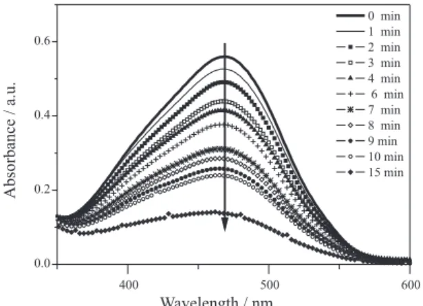
Figure 9 presents the results of the absorbance measurements as a function of wavelength for the system
composed of dye/H2O2/film. It is possible to observe the
decrease in intensity of the band situated at 469 nm with increasing UV exposure time.
Similar curves were obtained for the system without tungsten oxide films and the system containing tungsten oxide films obtained at Ts = 350 °C. When the efficiency in photocatalysis is concerned, the photon flux is important in determining the number of electrons that are generated, and hence the efficiency in creating an electron/hole pair. In this case the systems were irradiated with and without film in the same conditions, and these conditions imply the same photon flux and irradiated area. So, the efficiency of photocatalysis is proportional to the apparent rate constant, as can be seen through equation 2:
(2)
where kapis the apparent velocity constant, Cdye is the initial
dye concentration, Fph is the photon flux and A the irradiated
area. In our experiment, we observed constant A, Fph and
Cdye, so the efficiency ε is proportional to kap.
Photocatalytic degradation of the MO dye by the WO3
semiconductor under light irradiation typically includes two mechanisms. The first is based on the light excitation of the semiconductor, which forms electron/hole pairs (electrons in the conduction band and holes in the valence band). Chemical reactions with the organic compound take place as generated charges move to the particle surface. The second mechanism is based on the excitation of the dye and electrons are transferred from the dye to an electron acceptor. A cationic dye radical is formed which is followed
Figure 8.16O(α,α’)16O excitation curves at distinct depths for the WO 3
films obtained after the deposition time of 90 min: (a) 350 °C and (b) 600 °C.
Figure 9. Absorbance as a function of wavelength for the MO dye/H2O2
Table 4. Apparent velocity constant for MO degradation in the presence of H2O2 and UV (250 nm) radiation with and without tungsten oxide thin film obtained at different substrate temperatures
Condition kap / min-1 R
Without catalyst 7.2 × 10⁻² 0.991
350 °C 1.22 × 10⁻¹ 0.995
600 °C 1.11 × 10⁻¹ 0.998
Figure 10. First order fit for photodegradation of the methyl orange dye at 25 °C in the presence of H2O2 and UV (250 nm) radiation.
by self-degradation. The photocatalytic degradation follows a pseudo-first-order reaction. Its kinetics can be expressed using equation 3:
(3)
where C0 the initial concentration of organic dye, t is the
reaction time and Ct is the concentration of dye at the
reaction time t. Results are shown in Figure 10 and the
calculated kap values are presented in Table 4.
Conclusions
In this work, controlled substrate temperature and oxygen atmosphere allowed the obtainment of tungsten
oxide films with WO3.1 stoichiometry on Au/Si substrate
via thermal evaporation at low pressure.
Substrate temperature was important to define morphological aspects of the films. There was no specific grain morphology in samples obtained at lower substrate temperatures, while at higher temperatures the grains grew on well-defined shapes of up to 850 nm of diameter. SEM and TEM, as well as micro-Raman analyses, allowed the assignment of the growth process to the Stranski-Krastanov nanostructuring model.
Both analyzed temperatures promoted the formation of hexagonal tungsten oxide, but the presence of hydrated tungsten oxide species was also observed.
Films obtained at both temperatures did not lixiviate when exposed to slightly acidic aqueous solution, indicating success in the obtainment of a tungsten oxide matrix with good adhesion to the Au/Si substrate and resistant to exposure to aqueous media.
No significant influence of the substrate temperature on the performance of the photocatalyst synthesized in this work was observed. We can state, however, that the thin films obtained through thermal evaporation accelerate photolysis of the methyl orange dye by about ten times compared to the sample without catalyst.
Acknowledgement
The authors thank MCTI/CNPq/MEC/CAPES (CNPq/552197/2011-4 - Casadinho/Procad) and PROPESQ/UFRGS for the financial support.
References
1. Liao, C. H.; Huang, C. W.; Wu, J. C. S.; Catalysts 2012,2, 490. 2. Miyauchi, M.; Nakajima, A.; Watanabe, T.; Hashimoto, K.;
Chem. Mater. 2002,14, 2812.
3. Lambert-Mauriat, C.; Oison, V.; Saadi, L.; Aguir, K.; Surf. Sci. 2012,606, 40.
4. Hong, S. J.; Jun, H.; Borse, P. H.; Lee, J. S.; Int. J. Hydrogen. Energy 2009,34, 3234.
5. Peng, T.; Ke, D.; Xiao, J.; Wang, L.; Hu, J.; Zan, L.; J. Solid State Chem. 2012,194, 250.
6. Szilágyi, I. M.; Fórizs, B.; Rosseler, O.; Szegedi, Á.; Németh, P.; Király, P.; Tárkányi, G.; Vajna, B.; Varga-Josepovits, K.; László, K.; Tóth, A. L.; Baranyai, P.; Leskelä, M.; J. Catal. 2012,294, 119.
7. Martinez-de la Cruz, A.; Martinez, D. S.; Cuellar, E. L.; Solid State Sci. 2010,12, 88.
8. Fraga, L. E.; Zanoni, M. V. B.; J. Braz. Chem. Soc. 2011, 22,
718.
9. Houweling, Z. S.; Geus, J. W.; de Jong, M.; Harks, P. P. R. M. L.; van der Werf, K. H. M.; Schropp, R. E. I.; Mater. Chem. Phys. 2011,131, 375.
10. Van Hieu, N.; Van Vuong, H.; Van Duy, N.; Hoa, N. D.; Sens. Actuators, B 2012,171, 760.
11. Park, S.; Kim, H.; Jin, C.; Choi, S. W.; Kim, S. S.; Lee, C.;
Thermochim. Acta 2012,542, 69.
12. Vidyarthi, V. S.; Hofmann, M.; Sayan, A.; Sliozberg, K.; Konig, D.; Beranek, R.; Schuhmann, W.; Ludwig, A.; Int. J. Hydrogen. Energy 2011,36, 4724.
13. Yang, L.; Ge, D.; Zhao, J.; Ding, Y.; Kong, X.; Li, Y.; Sol. Energy Mater. Sol. Cells 2012,100, 251.
Winter, J.; Ludwig, A.; Fischer, R. A.; Devi, A.; Thin Solid Films 2011, 522, 11.
15. Ponzoni, A.; Comini, E.; Ferroni, M.; Sberveglieri, G.; Thin Solid Films 2005,490, 81.
16. Schmitz, J. E. J.; Chemical Vapor Deposition of Tungsten and Tungsten Silicides for VLSI/ ULSI Applications, 1st ed.; William Andrew: New York, US, 1992.
17. Wong, H. Y.; Ong, C. W.; Kwok, R. W. M.; Wong, K. W.; Wong, S. P.; Cheung, W. Y.; Thin Solid Films 2000, 376, 131. 18. Leftheriotis, G.; Papaefthimiou, S.; Yianoulis, P.; Siokou, A.;
Thin Solid Films 2001,384, 298.
19. Sucasaire, W.; Matsuoka, M.; Lopes, K. C.; Mittani, J. C. R.; Avanci, L. H.; Chubaci, J. F. D.; Added, N.; Trava, V.; Corat, E. J.; J. Braz. Chem. Soc. 2006,17, 1163.
20. Wasa, K.; Kitabatake, M.; Adachi, H.; Sputtering of Compound Materials, 1st ed.; William Andrew: New York, 2004; p 531. 21. Kim, H.; Senthil, K.; Yong, K.; Mater. Chem. Phys. 2010,120,
452.
22. Boulova, M.; Lucazeau, G.; J. Solid State Chem. 2002,167, 425.
23. Aird, A.; Domeneghetti, M. C.; Mazzi, F.; Tazzoli, V.; Salje, E. K. H.; J. Phys.: Condens. Matter 1998,10, L569.
24. Liu, W. C.; Cai, W.; Meng, X. L.; Trans. Nonferrous Met. Soc. China 2006,16, s337.
25. Al-Kuhaili, M. F.; Al-Aswad, A. H.; Durrani, S. M. A.; Bakhtiari, I. A.; Sol. Energy 2012,86, 3183.
26. Al-Kuhaili, M. F.; Al-Aswad, A. H.; Durrani, S. M. A.; Bakhtiari, I. A.; Sol. Energy 2009,83, 1571.
27. Meda, L.; Dangerfield, A. M.; Jones, M. C.; White, C. M.; Navulla, A.; Jpn. J. Appl. Phys. 2012,51, 11PE06 .
28. Vourdas, N.; Papadimitropoulos, G.; Kostis, I.; Vasilopoulou, M.; Davazoglou, D.; Thin Solid Films 2012,520, 3614.
29. Park, N.-K.; Lee, Y. J.; Yoon, S. H.; Han, G. B.; Ryu, S. O.; Lee, T. J.; Lee, W. G.; Bae, Y. J.; Scr. Mater. 2008,59, 328.
30. Luo, J. Y.; Zeng, Q. G.; Long, Y. B.; Wang, Y.; J. Nanosci. Nanotechnol. 2013,13, 1372.
31. Senthilkumar, R.; Ravi, G.; Sanjeeviraja, C.; Arivanandan, M.; Hayakawa, Y. In Solid State Physics, vol. 1512; Chauhan, A. K.;
Murli, C.; Gadkari, S. C., eds.; American Institute of Physics: Melville, 2013.
32. Nunes, M. R.; Perez, G. M.; Loguercio, L. F.; Alves, E. W.; Carreno, N. L. V.; Martins, J. L.; Garcia, I. T. S.; J. Braz. Chem. Soc. 2011,22, 2027.
33. Zhang, L.; Cao, X.-F.; Chen, X. T.; Xue, Z. L.; J. Colloid Interface Sci. 2011,354, 630.
34. Taffarel, S. R.; Lansarin, M. A.; Moro, C. C.; J. Braz. Chem. Soc. 2011,22, 1872.
35. Szilágyi, I.; Sajó, I.; Király, P.; Tárkányi, G.; Tóth, A.; Szabó, A.; Varga-Josepovits, K.; Madarász, J.; Pokol, G.; J. Therm. Anal. Calorim. 2009,98, 707.
36. Huang, C. C.; Huang, C. H.; Kuo, I. T.; Chau, L. K.; Yang, T. S.;
Colloids Surf., A 2012,409, 61.
37. Ramana, C. V.; Utsunomiya, S.; Ewing, R. C.; Julien, C. M.; Becker, U.; J. Phys. Chem. B 2006,110, 10430.
38. Lee, S.-H.; Cheong, H. M.; Liu, P.; Smith, D.; Tracy, C. E.; Mascarenhas, A.; Roland Pitts, J.; Deb, S. K.; Electrochim. Acta 2001,46, 1995.
39. Daniel, M. F.; Desbat, B.; Lassegues, J. C.; Gerand, B.; Figlarz, M.; J. Solid State Chem. 1987,67, 235.
40. Santato, C.; Odziemkowski, M.; Ulmann, M.; Augustynski, J.;
J. Am. Chem. Soc. 2001,123, 10639.
41. Chen, H. C.; Jan, D. J.; Chen, C. H.; Huang, K. T.; Electrochim. Acta 2013, 93, 307.
42. Szilágyi, I. M. S.; Madarász, J. N.; Pokol, G. R.; Király, P. T.; Tárkányi, G. B.; Saukko, S.; Mizsei, J. N.; Tóth, A. L.; Szabó, A. S.; Varga-Josepovits, K.; Chem. Mater. 2008,20, 4116.
Submitted: November 12, 2013