Resistivity Reduction of Nanostructured Undoped Zinc Oxide thin Films for Ag/ZnO
Bilayers Using APCVD and Sputtering Techniques
Navid Najafia Seyed Mohammad Rozatia*
Received: October 15, 2017; Revised: December 14, 2017; Accepted: February 07, 2018
Nanostructured undoped zinc oxide (ZnO) thin films were deposited using atmospheric pressure chemical vapor deposition (APCVD) on glass substrates using zinc acetate dehydrate [C4H6O4Zn·2H2O,
ZnAc] in less than 2 minutes for each sample. In order to reduce the resistivity of ZnO films, a very thin layer of Ag was deposited on top of the films via the sputtering method to reduce resistivity from 2.89 to 0.31 Ω.cm, using only a 30Å silver coating. Structural, electrical and optical properties of the resulting bilayers were also investigated. The results show a polycrystalline structure in higher temperatures compared to rather amorphous ones in lower temperatures such as 325℃. The XRD patterns of the optimum polycrystalline films were identified as a hexagonal wurtzite structure of ZnO with the (002) preferred orientation. Also, sheet resistance decreased from 17.8 MΩ/ to 28.9 KΩ/ for the temperatures of 325℃ to 450℃, respectively. Based on the physical properties of undoped ZnO, substrate temperature is an important factor which affects the crystallite size and modifies electrical parameters. UV-vis measurements revealed a reduction in the transparency of the layers with increasing substrate temperature. A sharp cut-off was observed in ultraviolet regions at around 380 nm.
Keywords: Zinc oxide, Silver, Chemical vapour deposition (CVD), Sputtering, Electrical resistivity, Bilayers.
*e-mail: smrozati@guilan.ac.ir
1. Introduction
Zinc oxide (ZnO) is a wide-band-gap (3.37 eV) semiconductor with a large (60 meV) exciton binding energy. It is fairly stable both chemically and physically. Its piezoelectricity and high room temperature electron mobility of 155 cm2 V-1 s-1 causes lasing action
based on exciton recombination above the room temperature. ZnO has received considerable attention because of its effect in fundamental studies and diverse applications in ultraviolet and blue light-emitting diodes, laser diodes, ferroelectrics, piezoelectrics, gas sensors, field-effect transistors, acoustic wave devices, solars,
and so on 1-6. ZnO has a wurtzite structure, which is, in fact, a
hexagonal crystal structure (lattice parameters: a=b=0.32427 nm, c=0.51948 nm), fitting to the space group P63mc, and is
identified by two interconnecting sublattices of O2- and Zn2+, in
a way that Zn ions are surrounded by O ions, and vice versa 7.
ZnO is fabricated by various methods such as sputtering 8,
spray pyrolysis 9-13, sol-gel 14, thermal oxidation 15, pulsed laser
deposition (PLD) 16,17, thermal evaporation 18, spin coating 19,
chemical vapor deposition (CVD) 20-22. ZnO can exist in one, two, or three dimensional structures, giving one of the most considerable collections of diverse particle structures in all materials 23.
Manufacturing as low as possible sheet resistance while maintaining the visible transparency is the main objective of many researches carried out on TCOs. According to Chen et. al
24, there is a lower limit for resistivity (or upper limit for charge
carriers' mobility) due to scattering mechanisms. Bellingham et. al 25 suggested 4 х 10-7 Ω.m as the absolute TCO resistivity lower
limit. The thickness of TCO is very crucial to many applications. Therefore, adding a few nanometers of a second layer of a good conductor (such as a metal) might be a reasonable way to keep the resistivity low without increasing the TCO thickness or losing high percentage of optical transparency. Silver is the best candidate because of having the lowest resistivity among metals 26.
The CVD of films and coatings contains the chemical reactions of reactants in a gaseous phase on or in close vicinity of an already heated substrate surface. This atomistic deposition process can provide highly pure materials with a good structural control at a nanometer or atomic scale level 27.
Atmospheric pressure CVD is an economic method, but has certain difficulties in the process control and most research considerations have been dedicated to low pressure CVD (LPCVD) and sputtering deposition which are, low pressure techniques for deposition. However, because of its potential for mass production, the APCVD of ZnO has been considered 28.
ZnO films manufactured by APCVD with a zinc source such as zinc acetylacetonate (Zn(C5H7O2)2) or zinc acetate
are chemically stable in air atmospheric pressure and are used as a precursor instead of diethyl zinc and dimethyl
zinc 29. Atmospheric CVD is advanced by the production
of active precursor vapors via gas-phase reactions. They diffuse through a thin hydrodynamic boundary film above the substrate. Because of the low reactivity of oxygen or metal precursors, temperatures above 300℃ for the substrate are needed for surface reactions, activating the gas-phase, and having high rates of film growth 30.
2. The Experiment
In this work, we used a homemade CVD apparatus to deposit ZnO films in atmospheric pressure (See Fig. 1) 31.
(3)
(4)
Lin et al. considered the thermal process of zinc acetate dihydrate as the dehydration, vaporization/decomposition, and formation of ZnO 33. The gaseous by-products desorb from the surface, starting to diffuse into the stream and transported by the carrier gas 34. Then, they must be ventilated by a chemical fume hood 35 in order to be safe for the environment.
In Set 2: a very thin Ag layer of a few angstrom as the second layer was sputtered in the vacuum condition using the DSR sputter vacuum coating sputtering system which employed a 2-inch-diameter magnetron silver target. The sputtering system had a film thickness monitor using a quartz crystal microbalance which was included a 6 MHz quartz crystal.
The transmittance spectra were recorded using a UV-vis spectrophotometer (Perkin-Elmer Lambda 25 UV/vis) in the range of 350-1100 nm. The electrical properties of thin films were measured by the Hall effect and Van der Pauw setup (RH 2010 PhysTech System). X-ray diffraction (XRD) was applied to determine the crystalline quality of the samples using Cu Kα radiation (model Philips PW-1800). Field emission scanning electron microscopy (FESEM) was carried out by a Mira 3-XMU equipped with an energy dispersive X-ray (EDX) system for the morphological analysis of the thin films. The Swanepoel method 36 was employed for thickness measurements of the samples with interference fringes and FESEM cross-section for interference-free thin films.
3. Results and Discussion
3.1 Structural properties
The XRD pattern on the ZnO thin films for different temperatures is demonstrated in Fig. 2. The peaks correlated with the theoretical ZnO patterns of Joint Committee on Powder Diffraction Standards (JCPDS), reference code 01-075-0576, indexed as a hexagonal wurtzite structure with no impurities. In the wurtzite structure of ZnO, the a- and c- axes of the orientation corresponded to (100) and (002) peaks.
At low temperatures, the atomic mobility is low which restricts the crystal growth 37 and a weak peak of (100) is dominated. The lowest sheet resistance is at 450℃ in which we have the highest carrier mobility. As Ardyanian et al. 38 suggested, this temperature in the best substrate temperature for ZnO deposition, because atoms have optimum energy for chemical reactions. By increasing the temperature up to 500℃, adatoms receive enough thermal energy and mobility increase which causes the growth of (002) preferred orientation 37. Hyun et al. 39 stated that the main effect of a change in composition
(
)
(
)
Zn CH COO
3 2+
2
H O
2$
Zn CH COO
3 2+
2
H O
2-( ) ( )
Zn CH COO H O Zn O CH COO CH COOH
4 3 2+2 2 $ 4 3 6+2 3
-(
)
Zn O CH COO
4 3 6+
3
H O
2$
4
ZnO
+
6
CH COOH
3-(
)
Zn O CH COO
4 3 6$
4
ZnO
+
6
CH COCH
3 3-
+
3
CO
2-All of the samples were deposited on glass substrates (75 х 25 х 1 mm3) by the CVD technique in a tube through the oxidation of zinc acetate dihydrate [C4H6O4Zn·2H2O, ZnAc]
as the precursor. The initial mass of zinc acetate powder was 0.5 g for all the samples and was directly introduced in the reactor. The system contained a horizontal tabular furnace with the diameter of 80 mm and the length of approximately 1 m.
All substrates were put in a detergent solution and then rinsed with deionized water. Next, these glass substrates were ultrasonically cleaned with a mixture of deionized water and HCl acid for 20 minutes. The substrates were rinsed in deionized water again. To prevent the cleaned substrates from oxidization before the deposition, the substrates were heated, while a nitrogen flow was applied to clean the surface of the furnace tube before resuming the deposition process. The deposition duration for each sample was less than 2 minutes depending on the temperature. The less the temperature, the more time it takes to vaporize the fixed amount of 0.5 g as the precursor material. In general, source material, system geometry, and quantity all affect the local vapor pressure of the reactants present at the substrate and, therefore, the properties and morphology of the obtained films 32.
Two sets of experiments were conducted. In Set 1: the temperature of the source material was varied from 325℃ to 550℃ in steps of 25℃. Air was utilized as the source of oxygen. The zinc acetate dihydrate powder vapor entered the substrate at the atmospheric pressure, and undoped ZnO films were deposited on the substrate. By increasing the temperature from the room temperature, water (H2O) was vaporised from
50℃, as shown in the reaction Eq. (1). Other products in the gas phase such as acetone, carbon dioxide, and acetic acid started to appear when the temperature reached around 200℃. These materials reached their highest concentration at around 270℃, as shown in Equations (2)- (4). As the temperature rose, ZnO thin films were formed by the chemical reactions below:
(1)
from an oxygen-deficient material to a more stoichiometric zinc oxide is the (002) preferred orientation. This causes the sheet resistance to increase for temperatures above 450℃.
The growth rate of each crystallographic plane differs based on crystal orientation and surface energy. The (002) to (100) polar planes ratio of intensity (I002 / I100) can affect
the photocatalytic activity due to the ZnO polar planes' contribution in the formation of oxygen vacancies 40. The
full width at half maximum (FWHM), crystallite sizes, peak positions, and d-spacing are listed in Table 1 (calculated by the PANalytical X'pert Highscore Plus software). Based on the XRD patterns, the dominant orientation of (002) was at 2θ ≈ 34º which is in agreement with a few other works
14,41-44. The other observed peaks were (100), (101), and (110).
Hence, the crystallites were highly oriented with their c-axes which are perpendicular to the substrate plane 45.
Average crystallite size was calculated by the Scherrer's
equation (5),
(5)
where λ=1.542 Å is the X-ray wavelength, β is the FWHM of the diffraction in radians, and Ɵ is the Bragg diffraction angle 46,47.
Inter-planar spacing (d) was measured using the following
equation 48
(6)
3.2 Morphological properties
The surface morphology of the thin films was observed using a field emission scanning electron microscope at room temperature. Fig. 3 illustrates FESEM micrographs of ZnO structures deposited on a glass substrate at four different temperatures. By comparing the images, the role of the deposition temperature is vivid. The surface morphology of ZnO thin films grown at a low substrate temperature (325℃) showed small crystallites with a high density. By increasing the temperature to 525℃, the crystallinity of the thin films was enhanced and we obtained the largest crystallites.
Table 1. Structural properties of ZnO thin films prepared at different substrate temperatures
Temperature (°C) Plane (hkl)
Bragg's angle
(2θ)
d-spacing
(Å) FWHM (2θ) Crystallite size (nm)
375
(100) 31.85 2.81 0.16 91.69
(002) 34.53 2.60 0.31 46.15
(101) 36.37 2.47 0.31 46.39
425
(100) 31.91 2.80 0.28 52.39
(002) 34.50 2.60 0.22 67.12
(101) 36.32 2.47 0.24 61.84
450
(100) 31.92 2.80 0.31 45.84
(002) 34.58 2.59 0.26 56.82
(101) 36.31 2.47 0.20 74.21
475
(100) 31.85 2.81 0.28 52.38
(002) 34.45 2.60 0.28 52.74
(101) 36.31 2.47 0.31 46.38
500 (002) 34.11 2.63 0.08 184.45
525 (002) 34.71 2.58 0.08 184.75
. / cos
D=0 9m b i
d
a
h
hk
k
l
c
1
4
3
2 2
2 2 2
2
=
T+
+
Y+
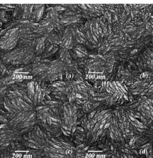
The morphology of grown ZnO with different thicknesses of Ag nanoparticle coating is depicted in Fig. 4. Slight changes were observed in the microstructure that can be attributed to the role of Ag thickness. As can be seen, the distribution of Ag nanoparticles over the ZnO layer was found to be relatively uniform.
EDX was implemented in different areas of the samples which confirmed the chemical composition of ZnO, as can be seen in Fig. 5. Table 2 shows the quantitative EDX results
Figure 2. The XRD pattern of undoped zinc oxide thin films deposited
at different substrate temperatures
Figure 3. FESEM images of undoped ZnO films deposited at (a)
for undoped zinc oxide thin films prepared at optimum temperature 450℃. Fig. 6 demonstrates the silver appearance in ZnO/Ag bilayers in the EDX spectrum. Table 3 shows the quantitative EDX results for ZnO/Ag bilayer thin films.
Figure 5. EDX spectrum measured for undoped zinc oxide thin films prepared at optimum temperature 450℃
Table 2. Quantitative EDX results for undoped zinc oxide thin films prepared at optimum temperature 450°C.
Elt Line Int Error K Kr W% A% ZAF Ox% Pk/Bg Class LConf HConf Cat#
O Ka 199.7 4.1979 0.1627 0.1315 25.97 58.90 0.5063 0.00 38.77 A 25.30 26.64 0.00
Zn Ka 216.6 0.7341 0.8373 0.6767 74.03 41.10 0.9140 0.00 26.85 A 72.19 75.87 0.00
1.0000 0.8081 100.00 100.00 0.00 0.00
Table 3. Quantitative EDX results for ZnO/Ag bilayer thin films.
Elt Line Int Error K Kr W% A% ZAF Ox% Pk/Bg Class LConf HConf Cat#
O Ka 98.9 4.0334 0.1053 0.0895 18.70 48.56 0.4786 0.00 41.49 A 18.02 19.39 0.00
Zn Ka 175.6 0.6631 0.8865 0.7540 80.42 51.10 0.9376 0.00 27.42 A 78.20 82.63 0.00
Ag La 6.3 1.8370 1.0000 0.8505 100.00 100.000.0082 0.0070 0.88 0.34 0.7963 0.000.00 2.34 B 0.75 1.00 0.000.00
Figure 4. FESEM micrographs showing ZnO/Ag bilayer surfaces
with different Ag thicknesses (a) 5 Å, (b) 10 Å, (c) 20 Å, (d) 30 Å
Figure 6. EDX spectrum measured for ZnO/Ag bilayer thin films
3.3 Electrical properties
If close to stoichiometry, ZnO films, show very high sheet resistance, while nonstochiometric ZnO films exhibit low sheet resistance. The electrical characteristics of ZnO thin films are mainly dominated by electrons which are generated from Zn interstitial atoms and oxygen vacancies 49. As in many other semiconductors, the conductivity of ZnO increases with increasing the
temperature 50.
Hall effect measurements were conducted using van der Pauw method with the magnetic field of 0.56 T. The samples were cut into square shapes (5 х 5 mm2). Silver dots were
formed as electrodes at the surfaces corners of each sample. Variations in sheet resistance, resistivity, Hall Co., mobility, and carrier concentration at different substrate temperatures are listed in Table 4. The lowest sheet resistance was achieved at 450℃.
Table 4. Electrical properties of ZnO thin films prepared at different substrate temperatures.
Temp. [°C] Sheet Resistance [Ω/] Resistivity[Ω.cm] [cmHall Co.3/As] Mobility[cm2/Vs]
Carrier Concentration [cm-3]
325 1.78 x 10⁷ 2460 -9520 3.88 6.55 x 10¹⁴
350 5.88 x 10⁶ 810 -6480 7.99 9.64 x 10¹⁴
375 8.92 x 10⁶ 1230 -9780 7.93 6.39 x 10¹⁴
400 3.44 x 10⁶ 474 -1270 2.68 4.92 x 10¹⁵
425 1.35 x 10⁶ 186 -147 0.79 4.24 x 10¹⁶
450 2.89 x 10⁴ 3.98 -2.54 0.64 2.46 x 10¹⁸
475 8.47 x 10⁴ 6.11 -10.3 1.69 6.04 x 10¹⁷
500 1.20 x 10⁶ 86.5 -43.5 0.50 1.43 x 10¹⁷
525 3.05 x 10⁷ 2200 -2820 1.28 2.21 x 10¹⁵
550 3.05 x 10⁷ 2200 -13200 6.01 4.73 x 10¹⁴
Table 5. Electrical properties of ZnO/Ag bilayers prepared at 450 °C with different Ag thicknesses.
Temp. [°C]
Ag layer thickness
[Å]
Sheet Resistance
[Ω/] Resistivity [Ω.cm] [cmHall Co.3/As] [cmMobility2/Vs]
Carrier Concentration
[cm-3]
450 0 2.89 x 10⁴ 3.98 -2.54 0.64 2.46 x 10¹⁸
450 5 6967 0.96 2.10 2.19 2.98 x 10¹⁸
450 10 5370 0.74 4.55 6.10 1.37 x 10¹⁸
450 20 3411 0.47 4.04 8.65 1.54 x 10¹⁸
450 30 2250 0.31 5.88 10.94 1.20 x 10¹⁸
Figure 7. Variations of resistivity, mobility and carrier concentration
versus deposition temperature
Fig. 7 shows sheet resistance, mobility, and carrier concentration variations by substrate temperature.
3.4 Optical properties
Fig. 8 illustrates the optical transmittance spectra obtained from ZnO thin films, at the wavelengths ranging from 300-1100 nm, as a function of substrate temperature which plays an important role in film formation. We had a transmittance of about 80% in the visible section of the spectrum from 325℃ to the optimum temperature, i.e. 450℃. At higher temperatures, transmittance was reduced and we lost most interference fringes.
Figure 8. Optical transmittance spectra for ZnO films deposited
with different substrate temperatures
A sharp cut-off was observed in ultraviolet region at around 380 nm that is due to band edge absorption of ZnO in this area, the monodispersed nature 51, and
an almost uniform size of nanoparticles 52 which is also
observed by Look 53 and Zhang et al. 54 at 373 nm and
369 nm, respectively.
Optical constants such as refractive index, extinction coefficient, and absorption coefficient were calculated using the average transmittance in the visible range. The transmittance of the glass substrate was only Ts = 91.33%
in the visible range. Afterwards, the refractive index of the substrate, s=1.540754, was obtained using
(7)
According to the Swanepoel method 36 which is based on the study by Manifacier et al. 55 on making upper and lower
envelopes of the transmittance spectrum (see Fig. 10), the refractive index of the film n in the transparent, weak, and
medium absorption regions can be calculated using
(8)
where
for the transparent region and
(9)
for medium and weak absorption regions. Tm and
TM are thecorresponding minimum and maximum
transmittances at a certain wavelength, respectively. The thickness of the film was given by:
(10)
where n(λ1) and n(λ2) are the refractive indices at two
adjacent minimums (or maximums) at λ1 and λ2, respectively. The
fundamental equation for interference fringes is 2nd=mλ where m is an integer for the maximum and half integer for the minimum.
Figure 9. Optical transmittance spectra for undoped zinc oxide compared to ZnO/Ag bilayers deposited with different Ag thicknesses
(
)
s
1T 1T1
1 2
S S
=
+
-[
(
) ]
n
N
N
2s
2 12 12=
+
-(
) /
N
ss
1 2
T
2 2
m
=
+
+
(
) /
(
) /
N
2
s T
MT
MT T
M ms
1 2
2
=
-
+
+
/ [
( )
( )]
d
=
m m
1 22
m
1n
m
2-
m
2n
m
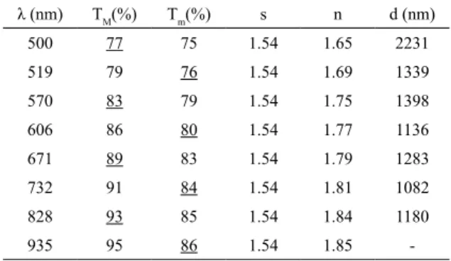
1The calculations of Table 6 correspond to the undoped ZnO sample deposited at 375℃ using Eq. (10) and the average thickness of 1378 nm was obtained for this sample. By increasing the deposition temperature, the thickness of the ZnO layers decreases which causes a decrease of grow rate 56.
The thickness of the film influences the optical transmission in which the number of interference fringes and the depth of these fringes depend on the film thickness57. Therefore, we
performed the Manifacier calculations for the sample with fringes (deposition temperature less than 475℃), resulting an average of 1300nm.
Figure 10. "Envelope method" graph including extremum values for thickness measurement
Table 6. The Manifacier’s calculations corresponding to the undoped
ZnO sample deposited at 375°C using Eq. (10)
λ (nm) TM(%) Tm(%) s n d (nm)
500 77 75 1.54 1.65 2231
519 79 76 1.54 1.69 1339
570 83 79 1.54 1.75 1398
606 86 80 1.54 1.77 1136
671 89 83 1.54 1.79 1283
732 91 84 1.54 1.81 1082
828 93 85 1.54 1.84 1180
935 95 86 1.54 1.85
-For layers with no or not enough interference fringes in the visible region of the transmission spectra, SEM cross-sections were utilized to measure the thickness of the layers. The average thickness for ZnO layers prepared at 475℃ and higher temperatures using SEM cross sections was 721 nm. For these films, the absorption coefficient can be calculated using a=( )1d ln( )1T 44,58-61, a=( )1d ln(100T)62 or
( ) ( )d ln
T T
1 0
a= 63 equations, where d is the film thickness, and
T and T0 are the transmittance of the ZnO thin film samples
of the film in the zone, we used Lambert's equation
( d) lnT 1
a= - 64.
Following the Swanepoel method, the absorption coefficient, α, and extinction coefficient, κ, can be obtained from TM and Tm, s and thickness by the following expressions, respectively 49.
(11)
(12)
Figs. 11 and 12 depict the absorption and extinction coefficients for samples prepared at different temperatures.
( )ln ( ) ( )
n n s
1
1 1
( )( ) t
n n s T T
T T 1
1 M m
M m
a= + + -
--
-# &
k
=
am4rFigure 11. Variations in absorption coefficient, α, as a function of
wavelength for ZnO films at different temperatures
Figure 12. Variations of extinction coefficient, κ, as a function of
wavelength for ZnO films at different temperatures
Optical transitions in semiconductor materials take place by direct and indirect transitions. The absorption coefficient, α, for direct transitions is expressed by Tauc's relation 65
(13)
where B is an energy-independent constant, α is the material's linear absorption coefficient, Eg is the optical band
gap and m is a constant which regulates the type of optical
transitions. For example, in an indirect allowed transition, m=2, for an indirect forbidden transition, m=3, for a direct allowed transition, m=1/2, and for a direct forbidden transition, m=3/2
48. In the graph, a straight line is fitted and the extrapolation
of this line E(=hν) axis shows the value of the band-gap. The plotted graphs for ZnO thin films with four different substrate temperatures and extrapolated Eg are shown in Fig. 13. The band-gaps of undoped ZnO films were more than 3.2 eV.
(
)
ahv
B hv
E
gm
=
-Figure 13. The dependence of (αhν)2 on photon energy E (=hν)
for different temperatures, from which the optical band gap (Eg) is estimated (Tauc's extrapolation)
4. Conclusion
In this work, we presented the synthesis of ZnO nanostructures prepared by atmospheric pressure CVD on glass substrates at different substrate temperatures in order to achieve the highest optical transparency and electrical conductivity. The optimum set of ZnO films were then used as a substrate for the second Ag layer to be sputtered on top of the first layer. Also, sheet resistance decreased from 17.8 MΩ/ to 28.9 KΩ/ for the temperatures of 325℃ to 450℃, respectively. Based on the physical properties of undoped ZnO, substrate temperature is an important factor which affects the crystallite size and modifies electrical parameters. UV-vis measurements revealed a reduction in the transparency of the layers with increasing substrate temperature. A sharp cut-off was observed in ultraviolet regions at around 380 nm.
5. Acknowledgements
6. References
1. Özgür Ü, Alivov YI, Liu C, Teke A, Reshchikov MA, Doğan S, et al. A comprehensive review of ZnO materials and devices. Journal of Applied Physics. 2005;98(4):041301. DOI: 10.1063/1.1992666
2. Pawar RC, Kim H, Lee CS. Improved field emission and photocatalysis properties of cacti-like zinc oxide nanostructures
Scripta Materialia. 2013;68(2):142-145. DOI: 10.1016/j.
scriptamat.2012.10.003
3. Yang J, Liu X, Yang L, Wang Y, Zhang Y, Lang J, et al. Effect of different annealing atmospheres on the structure and optical properties of ZnO nanoparticles. Journal of Alloys and Compounds.
2009;485(1-2):743-746. DOI: 10.1016/j.jallcom.2009.06.070
4. Li Z, Hu Z, Jiang L, Huang H, Liu F, Zhang X, et al. Synthesis and optical properties of three-dimensional nanowall ZnO film prepared by atmospheric pressure chemical vapor deposition.
Applied Surface Science. 2012;258(24):10175-10179. DOI:
10.1016/j.apsusc.2012.06.101
5. Liu WW, Yao B, Li YF, Li BH, Zhang ZZ, Shan CX, et al. Structure, luminescence and electrical properties of ZnO thin films annealed
in H2 and H2O ambient: A comparative study. Thin Solid Films.
2010;518(14):3923-3928. DOI: 10.1016/j.tsf.2009.12.099
6. Xu J, Pan Q, Shun Y, Tian Z. Grain size control and gas sensing properties of ZnO gas sensor. Sensors and Actuators B: Chemical.
2000;66(1-3):277-279. DOI: 10.1016/S0925-4005(00)00381-6 7. Benramache S, Belahssen O, Arif A, Guettaf A. A correlation
for crystallite size of undoped ZnO thin film with the band gap energy - precursor molarity - substrate temperature.
Optik - International Journal for Light and Electron Optics. 2014;125(3):1303-1306. DOI: 10.1016/j.ijleo.2013.08.015
8. Axelevitch A, Gorenstein B, Darawshe H, Golan G. Investigation of thin solid ZnO films prepared by sputtering. Thin Solid Films.
2010;518(16):4520-4524. DOI: 10.1016/j.tsf.2009.12.021 9. Lehraki N, Aida MS, Abed S, Attaf N, Attaf A, Poulain M. ZnO
thin films deposition by spray pyrolysis: Influence of precursor solution properties. Current Applied Physics.
2012;12(5):1283-1287. DOI: 10.1016/j.cap.2012.03.012
10. Mahajan CM, Takwale MG. Intermittent spray pyrolytic growth of nanocrystalline and highly oriented transparent conducting ZnO thin films: Effect of solution spray rate. Journal of Alloys and Compounds. 2014;584:128-135. DOI: 10.1016/j.jallcom.2013.08.136
11. Bacaksiz E, Yilmaz S, Parlak M, Varilci A, Altunbas M. Effects of annealing temperature on the structural and optical properties of ZnO hexagonal pyramids. Journal of Alloys and Compounds.
2009;478(1-2):367-370. DOI: 10.1016/j.jallcom.2008.11.025
12. Baneto M, Enesca A, Lare Y, Jondo K, Napo K, Duta A. Effect of precursor concentration on structural, morphological and opto-electric properties of ZnO thin films prepared by spray pyrolysis. Ceramics International. 2014;40(6):8397-8404.
DOI: 10.1016/j.ceramint.2014.01.048
13. Nunes P, Fernandes B, Fortunato E, Vilarinho P, Martins R. Performances presented by zinc oxide thin films deposited by spray pyrolysis. Thin Solid Films. 1999;337(1-2):176-179.
DOI: 10.1016/S0040-6090(98)01394-7
14. Caglar M, Ruzgar S. Influence of the deposition temperature on the physical properties of high electron mobility ZnO films by sol-gel process. Journal of Alloys and Compounds.
2015;644:101-105. DOI: 10.1016/j.jallcom.2015.04.167
15. Girtan M, Rusu GG, Dabos-Seignon S, Rusu M. Structural and electrical properties of zinc oxides thin films prepared by thermal oxidation. Applied Surface Science. 2008;254(13):4179-4185.
DOI: 10.1016/j.apsusc.2007.12.055
16. Wei XQ, Zhang ZG, Liu M, Chen CS, Sun G, Xue CS, et al. Annealing effect on the microstructure and photoluminescence of ZnO thin films. Materials Chemistry and Physics.
2007;101(2-3):285-290. DOI: 10.1016/j.matchemphys.2006.05.005
17. Pe´rez-Casero R, Gutie´rrez-Llorente A, Pons-Y-Moll O, Seiler W, Defourneau RM, Defourneau D, et al. Er-doped ZnO thin films grown by pulsed-laser deposition.
Journal of Applied Physics. 2005;97(5):054905. DOI:
10.1063/1.1858058
18. Yang XX, Lei W, Zhang XB, Wang BP, Li C, Hou K, et al. Growth and optical and field emission properties of flower-like ZnO nanostructures with hexagonal crown.
Thin Solid Films. 2009;517(15):4385-4389. DOI: 10.1016/j.
tsf.2009.01.056
19. Berber M, Bulto V, Kliß R, Hahn H. Transparent nanocrystalline ZnO films prepared by spin coating. Scripta Materialia.
2005;53(5):547-551. DOI: 10.1016/j.scriptamat.2005.04.047 20. Kashiwaba Y, Katahira F, Haga K, Sekiguchi T, Watanabe H.
Hetero-epitaxial growth of ZnO thin films by atmospheric pressure CVD method. Journal of Crystal Growth.
2000;221(1-4):431-434. DOI: 10.1016/S0022-0248(00)00729-6
21. Yoo YZ, Kim SH, Yoon GS, Choi EH, Park JW, Park JH, et al. Development of tilted hexagonal platelet ZnO using atmospheric pressure chemical vapor deposition and investigation of its growth mechanism. Applied Physics Letters. 2012;100(6):061909. DOI: 10.1063/1.3681163
22. de Graaf A, van Deelen J, Poodt P, van Mol T, Spee K, Grob F, et al. Development of atmospheric pressure CVD processes for highquality transparent conductive oxides.
Energy Procedia. 2010;2(1):41-48. DOI: 10.1016/j.
egypro.2010.07.008
23. Kolodziejczak-Radzimska A, Jesionowski T. Zinc Oxide-From Synthesis to Application: A Review. Materials.
2014;7(4):2833-2881. DOI: 10.3390/ma7042833
24. Chen M, Pei ZL, Wang X, Yu YH, Liu XH, Sun C, et al. Intrinsic limit of electrical properties of transparent conductive oxide films. Journal of Physics D: Applied Physics.
2000;33(20):2538-2548. DOI: 10.1088/0022-3727/33/20/304
25. Bellingham JR, Phillips WA, Adkins CJ. Intrinsic performance limits in transparent conducting oxides. Journal of Materials Science Letters. 1992;11(5):263-265. DOI: 10.1007/bf00729407 26. Lide DR, ed. Handbook of Chemistry and Physics. Boca Raton:
CRC Press; 1997.
27. Choy KL. Chemical vapour deposition of coatings. Progress in Materials Science. 2003;48(2):57-170. DOI:
28. van Deelen J, Illiberi A, Kniknie B, Beckers EHA, Simons PJPM, Lankhorst A. Atmospheric pressure chemical vapor deposition of ZnO: Process modeling and experiments. Thin Solid Films. 2014;555:163-168. DOI: 10.1016/j.tsf.2013.08.009
29. Pacio M, Juárez H, Escalante G, García G, Díaz T, Rosendo E. Study of (1 0 0) orientated ZnO films by APCVD system.
Materials Science and Engineering: B. 2010;74(1-3):38-41.
DOI: 10.1016/j.mseb.2010.04.030
30. Illiberi A, Poodt P, Bolt PJ, Roozeboom F. Recent Advances in Atmospheric Vapor-Phase Deposition of Transparent and Conductive Zinc Oxide. Chemical Vapor Deposition.
2014;20(7-8-9):234-242. DOI: 10.1002/cvde.201400056
31. Maleki M, Rozati SM. Structural, electrical and optical properties of transparent conducting SnO2 films: effect of the
oxygen flow rate. Physica Scripta. 2012;86(1):015801. DOI:
10.1088/0031-8949/86/01/015801
32. Djurišić AB, Ng AMC, Chen XY. ZnO nanostructures for optoelectronics: Material properties and device applications.
Progress in Quantum Electronics. 2010;34(4):191-259. DOI:
10.1016/j.pquantelec.2010.04.001
33. Lin CC, Li YY. Synthesis of ZnO nanowires by thermal decomposition of zinc acetate dihydrate. Materials Chemistry and Physics.
2009;113(1):334-337. DOI: 10.1016/j.matchemphys.2008.07.070 34. Gomez JL, Tigli O. Zinc oxide nanostructures: from growth to
application. Journal of Materials Science. 2012;48(2):612-624.
DOI: 10.1007/s10853-012-6938-5
35. Paraguay D F, Estrada L W, Acosta N DR, Andrade E, Miki-Yoshida M. Growth, structure and optical characterization of high quality ZnO thin films obtained by spray pyrolysis. Thin Solid Films.
1999;350(1-2):192-202. DOI: 10.1016/s0040-6090(99)00050-4
36. Swanepoel R. Determination of the thickness and optical constants of amorphous silicon. Journal of Physics E: Scientific Instruments. 1983;16(12):1214. DOI: 10.1088/0022-3735/16/12/023 37. Kang SJ, Joung YH, Shin HH, Yoon YS. Effect of substrate
temperature on structural, optical and electrical properties of ZnO thin films deposited by pulsed laser deposition. Journal of Materials Science: Materials in Electronics.
2008;19(11):1073-1078. DOI: 10.1007/s10854-007-9469-0
38. Ardyanian M, Bagheri-Mohagheghi MM, Sedigh N. Determination of the optimal parameters for the fabrication of ZnO thin films prepared by spray pyrolysis method. Pramana.
2012;78(4):625-634. DOI: 10.1007/s12043-011-0257-2
39. Yoon KH, Choi JW, Lee DH. Characteristics of ZnO thin films deposited onto Al/Si substrates by r.f. magnetron sputtering.
Thin Solid Films. 1997;302(1-2):116-121. DOI: 10.1016/
s0040-6090(96)09568-5
40. Hamdam Momen M, Amadeh A, Heydarzadeh Sohi M, Moghanlou Y. Photocatalytic properties of ZnO nanostructures grown via a novel atmospheric pressure solution evaporation method. Materials Science and Engineering: B.
2014;190:66-74. DOI: 10.1016/j.mseb.2014.09.002
41. Park NK, Lee YJ, Yoon SH, Han GB, Ryu SO, Lee TJ, et al. The epitaxial growth of ZnO nanowires for optical devices by a modified thermal evaporation method. Scripta Materialia.
2008;59(3):328-331. DOI: 10.1016/j.scriptamat.2008.03.042
42. Lupan O, Pauporté T, Chow L, Viana B, Pellé F, Ono LK, et al. Effects of annealing on properties of ZnO thin films prepared by electrochemical deposition in chloride medium. Applied Surface Science. 2010;256(6):1895-1907. DOI: 10.1016/j.
apsusc.2009.10.032
43. Lu JG, Kawaharamura T, Nishinaka H, Kamada Y, Ohshima T, Fujita S. Zno-based thin films synthesized by atmospheric pressure mist chemical vapor deposition. Journal of Crystal Growth. 2007;299(1):1-10. DOI: 10.1016/j.jcrysgro.2006.10.251
44. Gümüz C, Ozkendir OM, Kavak H, Ufuktepe Y. Structural and optical properties of zinc oxide thin films prepared by spray pyrolysis method. Journal of Optoelectronics and Advanced Materials. 2006;8(1):299-303.
45. Ilican S, Caglar M, Caglar Y. Determination of the thickness and optical constants of transparent indium-doped ZnO thin films by the envelope method. Materials Science-Poland. 2007;25(3):709-718.
46. Tsai YZ, Wang NF, Tsai CL. Fluorine-doped ZnO transparent conducting thin films prepared by radio frequency magnetron sputtering. Thin Solid Films. 2010;518(17):4955-4959. DOI:
10.1016/j.tsf.2010.03.086
47. Cullity BD, Stock SR. Elements of X-Ray Diffraction. 3rd ed.
Harlow: Pearson; 2001.
48. Yakuphanoglu F. Electrical characterization and device characterization of ZnO microring shaped films by sol-gel method. Journal of Alloys and Compounds.
2010;507(1):184-189. DOI: 10.1016/j.jallcom.2010.07.151
49. Bhat JS, Patil AS, Swami N, Mulimani BG, Gayathri BR, Deshpande NG, et al. Electron irradiation effects on electrical and optical properties of sol-gel prepared ZnO films. Journal of Applied Physics. 2010;108(4):043513. DOI: 10.1063/1.3452333
50. Moezzi A, McDonagh AM, Cortie MB. Zinc oxide particles: Synthesis, properties and applications. Chemical Engineering Journal. 2012;185-186:1-22. DOI: 10.1016/j.cej.2012.01.076
51. Talam S, Karumuri SR, Gunnam N. Synthesis, Characterization, and Spectroscopic Properties of ZnO Nanoparticles. ISRN Nanotechnology. 2012;2012:372505. DOI: 10.5402/2012/372505
52. Alwan RM, Kadhim QA, Sahan KM, Ali RA, Mahdi RJ, Kassim NA, et al. Synthesis of Zinc Oxide Nanoparticles via Sol - Gel Route and Their Characterization. Nanoscience and Nanotechnology. 2015;5(1):1-6. DOI: 10.5923/j.nn.20150501.01
53. Look DC. Recent advances in ZnO materials and devices.
Materials Science and Engineering: B. 2001;80(1-3):383-387.
DOI: 10.1016/S0921-5107(00)00604-8
54. Zhang XL, Hui KS, Hui KN. High photo-responsivity ZnO UV detectors fabricated by RF reactive sputtering. Materials Research Bulletin. 2013;48(2):305-309. DOI: 10.1016/j.
materresbull.2012.10.030
55. Manifacier JC, Gasiot J, Fillard JP. A simple method for the determination of the optical constants n, k and the thickness of a weakly absorbing thin film. Journal of Physics E: Scientific Instruments. 1976;9(11):1002. DOI: 10.1088/0022-3735/9/11/032
56. Bensmaine S, Benyoucef B. Effect of the Temperature on ZnO Thin Films Deposited by r.f. Magnetron. Physics Procedia.
57. Gungor T, Gungor E, Saka B. Fast and interference fringe independent optical characterization of zinc oxide nano thin films using model-based genetic algorithm for optoelectronic applications. Nanomaterials and Nanotechnology. 2016;6:1-7. DOI: 10.1177/1847980416673785
58. Joseph B, Manoj PK, Vaidyan VK. Studies on the structural, electrical and optical properties of Al-doped ZnO thin films prepared by chemical spray deposition. Ceramics International.
2006;32(5):487-493. DOI: 10.1016/j.ceramint.2005.03.029
59. Thonglem S, Intatha U, Eitssayeam S. Effect of magnesium and fluorine dopants on properties of ZnO thin films. Ceramics International.
2015;41(Suppl 1):S331-S336. DOI: 10.1016/j.ceramint.2015.03.215 60. Wu M, Yu S, Chen G, He L, Yang L, Zhang W. Structural,
optical, and electrical properties of Mo-doped ZnO thin films prepared by magnetron sputtering. Applied Surface Science.
2015;324:791-796. DOI: 10.1016/j.apsusc.2014.11.039
61. Hu D, Liu X, Deng S, Liu Y, Feng Z, Han B, et al. Structural and optical properties of Mn-doped ZnO nanocrystalline thin films with the different dopant concentrations. Physica E: Low-dimensional Systems and Nanostructures. 2014;61:14-22. DOI: 10.1016/j.physe.2014.03.007
62. Zunke I, Heft A, Schäfer P, Haidu F, Lehmann D, Grünler B, et al. Conductive zinc oxide thin film coatings by combustion chemical vapour deposition at atmospheric pressure. Thin Solid Films. 2013;532:50-55. DOI: 10.1016/j.tsf.2012.11.151
63. Shirazi M, Hosseinnejad MT, Zendehnam A, Ghoranneviss M, Reza Etaati G. Synthesis and characterization of nanostructured ZnO multilayer grown by DC magnetron sputtering. Journal of Alloys and Compounds.
2014;602:108-116. DOI: 10.1016/j.jallcom.2014.03.029
64. Choi YJ, Park HH. A simple approach to the fabrication of fluorine-doped zinc oxide thin films by atomic layer deposition at low temperatures and an investigation into the growth mode.
Journal of Materials Chemistry C. 2014;2(1):98-108. DOI:
10.1039/C3TC31478B
65. Tauc J, Menth A. States in the gap. Journal of Non-Crystalline Solids. 1972;8-10(1972):569-585. DOI: