Instrumentation Amplifier using
Differential voltage second generation
current conveyor (DVCCII) in standard
0.18
μ
m CMOS technology
Ashish Panchal (Student)
Electronics & Instrumentation Engg. Department,
Shri G.S.Institute of Technology and Science,
Indore, India
Mobile no.:-+919691243624
Pramod Kumar Jain (Associate Professor) Electronics & Instrumentation Engg. Department,
Shri G.S.Institute of Technology and Science,
Indore, India
Mobile no.:-+918878122571
D.S. Ajnar (Associate Professor) Electronics & Instrumentation Engg. Department,
Shri G.S.Institute of Technology and Science,
Indore, India
Mobile no.:-+919406681443
Abstract:-In this paper a new CMOS high performance, high frequency current mode signal DVCC-II is presented. Output stage AB amplifier provides high driving capability ±0.9mA. It provides rail to rail
input-output operation. The proposed DVCC-II has been designed in 0.18μm CMOS technology with 1.8V supply voltage. SPECTRA RF simulator is used for circuit simulation. In low voltage sub-micrometer analog circuit
accuracy and precision can be limited by the finite gain as well as by input offset voltage. Proposed circuit
features have high CMRR, high gain and bandwidth that can be achieved simultaneously without requiring well
matched register.
I. INTRODUCTION
Voltage based circuits depends on the voltage-feedback amplifier (voltage operational amplifier) have
disadvantage of severe reduce bandwidth at higher gains, because of operational amplifier’s fixed
gain/bandwidth product. An attempt to over come this problem, current conveyor is proposed by Sedra have
been acknowledged to be versatile building blocks for current mode signal processing. The first current
conveyor (CC-I) was introduced in 1968 and are rarely available.
Figure 1:- Current Conveyor
The original current conveyor is shown in figure 1. It is a three terminal device (two input terminals X and Y
and one output terminal Z).
A major problem that has hindered the monolithic IC implementation of CC-I has been, in earlier realizations,
the need for high quality PNP Transistors. To overcome this problem second generation current conveyor
(CC-II) proposed by Sedra and Smith in 1970.
In analog circuit design, many researches have been performed on current conveyor circuits, which have some
recognized advantages such as high performance in terms of speed, bandwidth, and accuracy. It is one of the
most versatile building blocks. It has been used in wide range of application and several circuit realizations have
been proposed for its implementation. The second generation current conveyor (CC-II) is single ended device,
however, fully differential circuit configuration have been widely used recently in high frequency analog
circuits.
Conveyor-based implementations offer improved performance to the voltage op-amp based implementations in
terms of accuracy, bandwidth, and convenience due to the inherent local feedback of the follower based
structure of the device and its very attractive combined voltage–current capabilities. The voltage–current
describing matrix of the CCII is given by
which indicates that the voltage at the low-impedance input node (X) follows the high-impedance input node
(Y), while the input current at node (X) is mirrored (conveyed) to the high-impedance output node (Z).
The remaining paper is organized as follows. In next section the proposed DVCC CMOS circuit realization and
II. PROPOSED DVCCCMOSCIRCUIT REALIZATION
A. Circuit Description:-
The circuit realization of the proposed DVCC (Fig. 2) is based on equalizing the output currents of two wide
linear range trans-conductors, formed by transistors (M1–M18). In addition, (M19–M22) comprise a Class-AB
output stage, providing current swings up to ±1mA. Moreover, the current at the X terminal is transferred to the
Z terminal with the aid of (M23, M24), which must before a unity current gain matched with (M21, M22),
respectively.
Figure2:- Schematic view of DVCC-II
All transistors are assumed to be operating in saturation. The operation of a wide linear range trans-conductor
relies mainly on biasing along tail differential pair LTDP (M1–M2) with a dynamic tail current Iss that increases
with V2 id where Vid = VY1 −VY2. Since the output current produced at the drains of M2 and M6 is expressed
by
Eq ... 1
Eq ... 2
Where k represents the trans-conductance parameter of M1 or M2, than if the tail current is set to
Eq ... 3
Hence, in order to increase the input range of the trans-conductor the ratio Iss/k should be increased.
Eq ... 4
Eq ... 5
So taking into account that the input signals of a differential pair can be divided into a common mode voltage
(VCM) and a differential voltage (Vid ) with VY1 = Vid/2 + VCM and VY2 =−Vid/2 + VCM where VCM = (VY1
For differential input voltages greater than twice the square root of 2IB/K13 M1 turns off and the current
flowing in M2 increases. On the other hand, as the differential input voltage is decreased below twice the square
root of 2IB/K13, M2 turns off and the current flowing in M1 increases. In both cases, M9 should feed the
necessary current required for proper operation of M1 and M2 even if it enters slightly in the linear region.
Therefore, the problem with the minimum common mode input voltage required to maintain the tail biasing
transistor in saturation has less effect in this circuit. Furthermore, since both M1 and M2 are ‘ON’ at standby,
this circuit exhibit slow distortion. It should be also noted that the current flowing in M9 will change by
feedback action, formed by M15, in order to stabilize the value of VS.
B. Symbolic Representation:-
Figure 3:- Symbolic Representation of DVCC-II
Figure 4:- Symbolic Representation of Instrumentation Amplifier
The figure 3 shows the symbolic representation of second generation current conveyor (DVCC-II). Y1, Y2, are
the inputs and Z is the output terminal. X terminal convey the current to the Z terminal. The gain of DVCC-II is
controlled by bias voltages VB1, VB2, and VB3.
The above expression is set to a constant value. Figure 4 shows the symbolic representation of instrumentation
amplifier
III. SIMULATION RESULTS
The performance of the proposed COMS DVCC is verified by performing SPECTRA RF simulation with
resistance. The DVCC shows good linearity for differential input voltages between ±0.9V, with a total standby
power dissipation of 1.12mW.
Figure 5:- DC Response for Positive Terminal
Figure 6:- DC Response for Negative Terminal
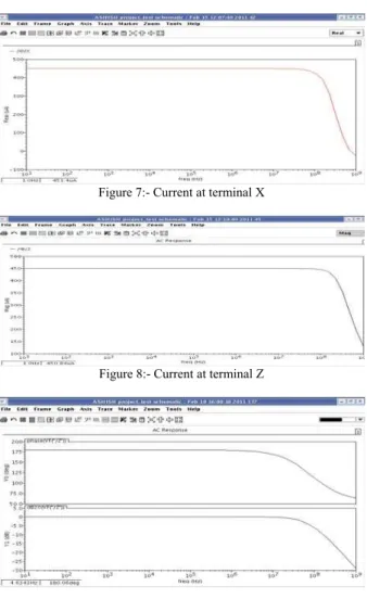
Figure 7:- Current at terminal X
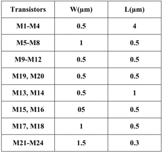
Figure 8:- Current at terminal Z
Figure 10:- Magnitude Response of Instrumentation Amplifier Gain (G = 1)
Figure 11:- Magnitude Response of Instrumentation Amplifier Gain (G = 2)
In Fig.7 magnitude and phase response of differential voltage current conveyor with differential input AC signal and open circuit output terminal is shown. The DVCC-II shows a flat response with 150MHz 3-dB bandwidth. For short circuit provides 350MHz 3-dB bandwidth.
Figure 12:- Magnitude Response of Instrumentation Amplifier Gain (G = 3)
Figure 13:- Magnitude Response of Instrumentation Amplifier Gain (G = 4)
The current at X terminal and output Z terminal is observed with load resistance of 4KΩ. Both terminal currents are of same value about 450µAas shown in Fig.8 and Fig.9.
Instrumentation amplifier takes a differential input voltage multiply with its gain and produces a single ended output voltage as shown in Fig.4. Relation between input and output can be described as:-
Table 1:- Transistor Aspect Ratio
Transistors W(µm) L(µm) M1-M4 0.5 4 M5-M8 1 0.5 M9-M12 0.5 0.5 M19, M20 0.5 0.5
M13, M14 0.5 1 M15, M16 05 0.5 M17, M18 1 0.5
M21-M24 1.5 0.3
IV. CONCLUSION
CMOS architecture for the DVCC-II was presented. Simulations have demonstrated that it is quite useful as a
building block of current-mode signal processing. A circuit has been presented that displays very attractive DC
and AC response and can be advantageously used to implement a large number of RF-controlled functions.
Modification to class AB, low power operation, is a future work.
V. REFERENCES
[1] Google Wikipedia
[2] Sedra A, Smith K. A second-generation current conveyor and its applications. IEEE Transactions on Circuit Theory 1970; 17:132–4.
[3] SEDRA, A.S, ROBERTS, G w., and GOHH, F: ‘the current conveyor: History, progress and new results’, IEE Proc. G, Circuits
Devices Syst., 1990, 137, (2), pp. 78-87.
[4] Mahmoud SA. Fully differential CMOS CCII based on differential difference trans-conductor. Analog Integrated Circuits and Signal Processing 2007; 50:195–203.
[5] Ismail AM, Soliman AM. Novel CMOS liberalized balanced output trans-conductance amplifier based on differential pairs. Frequenz 1999;53:170–4
[6] Mahmoud SA. Fully differential CMOS CCII based on differential difference trans-conductor. Analog Integrated Circuits and Signal Processing 2006; 49:267–79.
[7] YOU, F., EMBABI, S.H.K., and SANCHEZ-SINENCIO, E.: 'Low-voltage class AB buffers with quiescent current control', IEEE J.
Solid-State Circuits, 1998, 33, (6), pp. 915-919.
[8] FABRE, A, SAAID, O., WIEST. F. and BOUCHERON, C.: ‘High frequency application based on a new current controlled conveyor’,